Integrated
Circuit
Systems, Inc.
User-Programmable Dual High-Performance Clock Generator
ICS2595
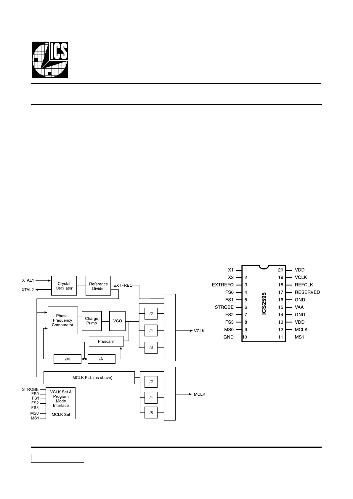
Pin Configuration
Block Diagram
ICS2595 RevB 3/2/00
20-Pin DIP or SOIC
Features
• Advanced ICS monolithic phase-locked loop
technology for extremely low jitter
• Supports high-resolution graphics - VCLK
output to 145 MHz
• Completely integrated - requires only external
crystal (or reference frequency and decoupling)
• Power-down modes support portable computing
• Sixteen selectable VCLK frequencies
(all user re-programmable)
• Four selectable MCLK frequencies
(all user re-programmable)
Description
The ICS2595 is a dual-PLL (phase-locked loop) clock
generator specifically designed for high-resolution, highrefresh rate, video applications. The video PLL generates
any of 16 pre-programmed frequencies through selection
of the address lines FS0-FS3. Similarly, the auxiliary PLL
can generate any one of four pre-programmed frequencies
via the MS0 & MS1 lines.
A unique feature of the ICS2595 is the ability to redefine
frequency selections in both the VCLK and MCLK synthesizers after power-up. This permits complete set-up of the
frequency table upon system initialization.
Applications
• PC Graphics
• VGA/Supper VGA/XGA Applications
Not recommended for new designs

2
ICS2595
Pin Descriptions
REBMUNNIP EMANNIP EPYT NOITPIRCSED
11XNItupnIycneuqerFecnerefeR/1noitcennoclatsyrcztrauQ
22XTUO2noitcennoclatsyrcztrauQ
3QERFTXENItupnIycneuqerFlanretxE
40SFNIBSLtceleSycneuqerFLLPKLCV
51SFNItiBtceleSycneuqerFLLPKLCV
6EBORTSNI)3SF-0SF(stitceleSKLCVfohctaLroflortnoC
72SFNItiBtceleSycneuqerFLLPKLCV
83SFNIBSMtceleSycneuqerFLLPKLCV
90SMNIBSLtceleSycneuqerFLLPKLCM
61,41,01DNGRWPdetcennocebtsumsnipllA.dnuorGeciveD
111SMNIBSMtceleSycneuqerFLLPKLCM
21KLCMTUOtuptuOycneuqerFKLCM
02,31DDVRWPdetcennocebtsumsnipllA.DDVegatStuptuO
51AAVRWPDDVrezisehtnyS
71DEVRESERC/NDNGotdetcennocebtsuM
81KLCFERTUOtuptuOkcolCdecnerefeRdereffuB
91KLCVTUOtuptuOycneuqerFKLCV

ICS2595
3
Digital Inputs
The FS0-FS3 pins and the STROBE pin are used to select
the desired operating frequency of the VCLK output from
the 16 pre-programmed/user-programmed selections in
the ICS2595. These pins are also used to load new frequency
data into the registers.
The standard interface for the ICS2595 matches the interface
of the industry standard ICS2494. That is, the FS0-FS3
inputs access the device internals transparently when the
STROBE pin is high.
The digital interface for the ICS2595 (i.e. the FS0-FS3
inputs) may be optionally configured for edge-triggered
or level-activated operation of the STROBE pin. Example
timing requirements for each of the four options are
shown in Figure 1.
The programming sequence has been designed in such a
way that STROBE pin need not be used (as in situations
where the device is connected to the frequency select port
of some VGA chips).
VCLK Output Frequency Selection
To change the VCLK output frequency, simply write the
appropriate data to the ICS2595 FS inputs. The synthesizer
will output the new frequency programmed into that location
after a brief delay (see time-out specifications).
Upon device power-up, the selected frequency will be the
frequency pre-programmed into address 0 until a device
write is performed.
MCLK Output Frequency Selection
The MS0-MS1 pins are used to directly select the desired
operating frequency of the MCLK output from the four
pre-programmed/user-programmed selections in the
ICS2595. These inputs are not latched, nor are they involved
with memory programming operations.
Programming Mode Selection
In order to ensure that reliable programming under all
circumstances, we require that two "nibble" writes be
added to the beginning of the programming sequence that
was previously specified. The new sequence is shown in
Table 1. Note that the FS3 data is "0" for these first two
writes.
elbbiN
0SF1SF2SF3SF
1X X 0 0
2X X 1 0
3X X )"0"ebtsum(tibTRATS0
4X X " 1
5X X
ebtsum(tiblortnoc*W/R
)"0"
0
6X X " 1
7X X )BSLnoitacol(OL0
8X X " 1
9X X 1L0
01X X " 1
11X X 2L0
21X X " 1
31X X 3L0
41X X " 1
51X X )BSMnoitacol(4L0
61X X " 1
71X X BSLkcabdeef(0N0
81X X " 1
91X X 1N0
02X X " 1
12X X 2N0
22X X " 1
32X X 3N0
42X X " 1
52X X 4N0
62X X " 1
72X X 5N0
82X X " 1
92X X 6N0
03X X " 1
13X X )BSMkcabdeef(7N0
23X X " 1
33X X )"1"fitceles(QERFTXE0
43X X " 1
53X X )BSMredvid-tsop(0D0
63X X " 1
73X X )BSMredvid-tsop(1D0
83X X " 1
93X X )"1"ebtsum(tib1POTS0
04X X " 1
14X X )"1'ebtsum(tib2POTS0
24X X " 1
T able 1: Programming Sequence
Because the same pins are used for both VCLK frequency
selection and re-programming the device frequency table,
a specific procedure must be observed for selection between
these modes. Device programming is accomplished by
executing a "programming sequence". The latched FS2
input functions as a data input, and the latched FS3 input
functions as a data clock when this mode is activated. As
the latched FS3 data transitions from 0 to 1, the latched
FS2 data is shifted into the register. Note that it is the

4
ICS2595
LATCHED FS inputs, not the FS inputs themselves, that
are interpreted by the internal logic. Interface logic resides
between the FS input pins and the programming/frequency
select logic. The appropriate "data write" procedure must
be observed. See the section "Digital Interface" in this
supplement for more information.
These rules must be followed:
• Calculate
T
max and Tmin in seconds (where R is the
modulus of the reference divider and Fref is the
reference frequency in Hz) by the following formulas:
• A programming sequence consists of 42 successive
data writes to the device as shown in table 1: no delay
greater than
T
max or less than Tmin may occur between
any two successive writes.
• A readback sequence consists of 64 successive data
writes to the device as shown in table 2: no delay
greater than Tmax or less than Tmin may occur between
any two successive writes.
• Programming or readback sequences must be preceded
by a "quiet" period of at least 2* Tmax with no data
writes to the device unless it was immediately preceded
by another legal programming (or readback) sequence
(nothing else in between)
• To change the active VCLK frequency selection, simply
write that data to the device; the last data written to the
part will always become VCLK frequency select after
a delay of approximately 2* Tmax. The internal shift
register is cleared at this time also.
The FS0 & FS1 inputs are not used for programming, so it
is possible to use a two-pin interface for programming and
frequency selection (any bank of four VCLK addresses).
The reference frequency source must be operational for
proper execution of the programming sequence. If the onchip crystal oscillator is, allow at least 4* Tmax after the
device has valid power before attempting to program it.
Data Description
Location Bits (l0-L4)
The first five bits after the start bit control the frequency
location to be re-programmed according to this table. The
rightmost bit (the LSB) of the five shown in each
selection of the table is the first one sent.
)0.4(LNOITACOL
000000sserddAKLCV
100001sserddAKLCV
010002sserddAKLCV
110003sserddAKLCV
001004sserddAKLCV
101005sserddAKLCV
011006sserddAKLCV
111007sserddAKLCV
000108sserddAKLCV
100109sserddAKLCV
0101001sserddAKLCV
1101011sserddAKLCV
0011021sserddAKLCV
1011031sserddAKLCV
0111041sserddAKLCV
1111051sserddAKLCV
000010sserddAKLCM
100011sserddAKLCM
010012sserddAKLCM
110014sserddAKLCM
Table 3 - Location Bit Programming
Feedback Set Bits (N0-N7)
These bits control the feedback divider setting for the
location specified. The modulus of the feedback divider
will be equal to the value of these bits + 257. The least
significant bit (N0) is sent first.
Post-Divider Set Bits (D0-D1)
These bits control the post-divider setting for the location
specified according to this table. The least significant bit
(D0) is sent first.
Table 4 - Post-Divider Programming
)0-1(DREDIVID-TSOP
008
104
012
111
T
min =
6* R
F
ref
T
max =
4096* R
F
ref
 Loading...