

1-248
H
CAUTION: It is advised that normal static precautions be taken in handling and assembly of this component to
prevent damage and/or degradation which may be induced by ESD.
HCPL-7840
Analog Isolation Amplifier
Technical Data
A 0.1 F bypass capacitor must be connected between pins 1 and 4 and between pins 5 and 8.
Features
• High Common Mode
Rejection (CMR): 15 kV/µs
at VCM = 1000 V
• 5% Gain Tolerance
• 0.1% Nonlinearity
• Low Offset Voltage and Offset Temperature Coefficient
• 100 kHz Bandwidth
• Performance Specified Over
-40°C to 85°C Temperature
Range
• Recognized Under UL 1577
and CSA Approved for
Dielectric Withstand Proof
Test Voltage of 2500 Vac, 1
Minute
• Standard 8-Pin DIP Package
Applications
• Motor Phase and Rail
Current Sensing
• Inverter Current Sensing
• Switched Mode Power
Supply Signal Isolation
• General Purpose Current
Sensing and Monitoring
• General Purpose Analog
Signal Isolation
Description
The HCPL-7840 isolation amplifier provides accurate, electrically
isolated and amplified representations of voltage and current.
When used with a shunt resistor
in the current path, the HCPL7840 offers superior reliability,
cost effectiveness, size and
autoinsertability compared with
the traditional solutions such as
current transformers and Halleffect sensors.
The HCPL-7840 consists of a
sigma-delta analog-to-digital
converter optically coupled to a
digital-to-analog converter.
Superior performance in design
critical specifications such as
common-mode rejection, offset
voltage, nonlinearity, operating
temperature range and regulatory
compliance make the HCPL-7840
the clear choice for designing
reliable, lower-cost, reduced-size
products such as motor
controllers and inverters.
Common-mode rejection of
15 kV/µs makes the HCPL-7840
suitable for noisy electrical
environments such as those
generated by the high switching
rates of power IGBTs.
Low offset voltage together with
a low offset voltage temperature
coefficient permits accurate use
of auto-calibration techniques.
Gain tolerance of 5% with 0.1%
nonlinearity further provide the
performance necessary for
accurate feedback and control.
A wide operating temperature
range with specified performance
allows the HCPL-7840 to be used
in hostile industrial environments.
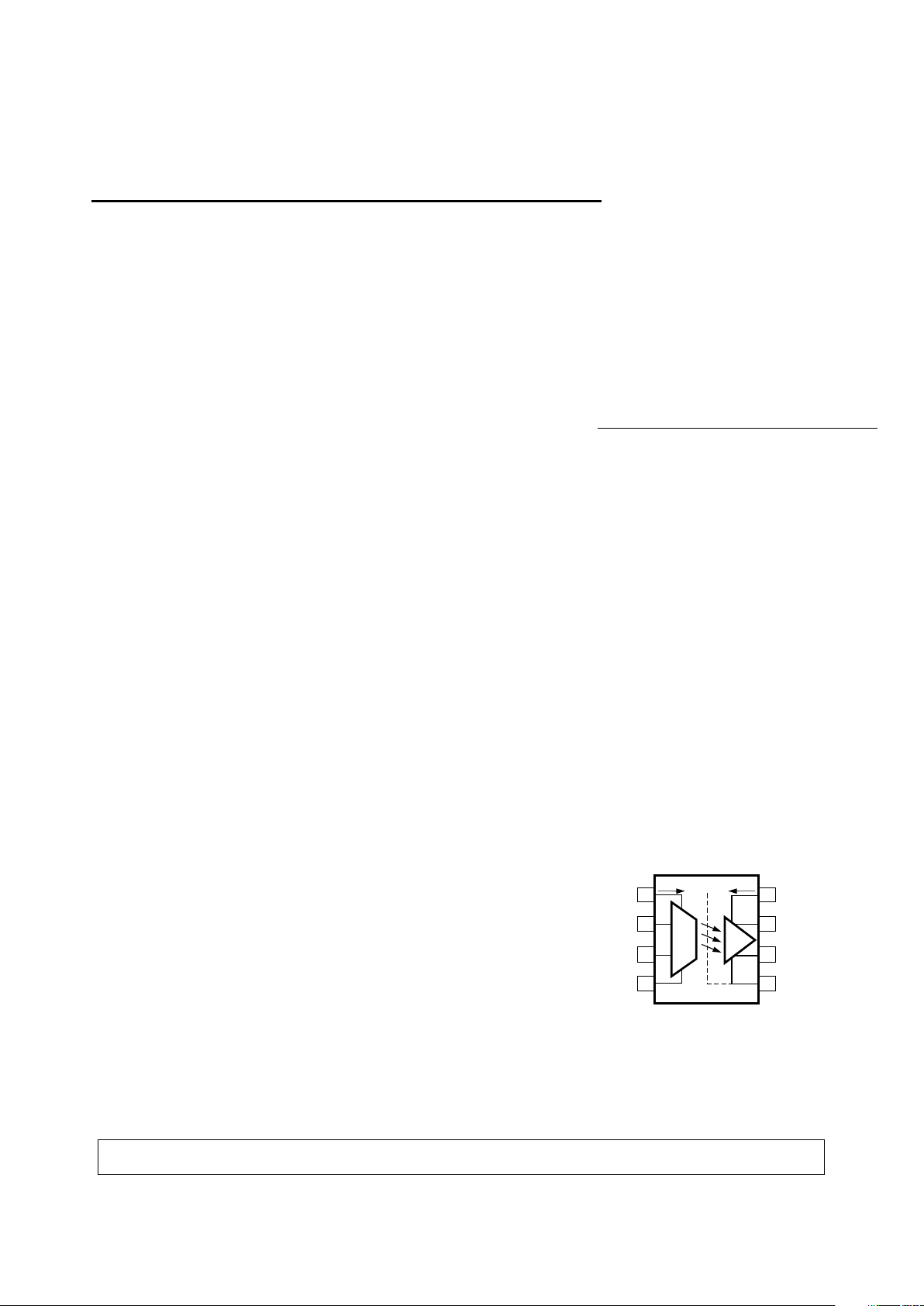
Functional Diagram
1
2
3
4
8
7
6
5
I
DD1
V
DD1
V
IN+
V
IN–
GND1
I
DD2
V
DD2
V
OUT+
V
OUT–
GND2
+
–
+
–
SHIELD
5965-4784E
1-249
Package Outline Drawings
Standard DIP Package
9.65 ± 0.25
(0.380 ± 0.010)
1.78 (0.070) MAX.
1.19 (0.047) MAX.
HP 7840
YYWW
DATE CODE
1.080 ± 0.320
(0.043 ± 0.013)
2.54 ± 0.25
(0.100 ± 0.010)
0.51 (0.020) MIN.
0.65 (0.025) MAX.
4.70 (0.185) MAX.
2.92 (0.115) MIN.
7.62 ± 0.25
(0.300 ± 0.010)
5° TYP.
5678
4321
6.35 ± 0.25
(0.250 ± 0.010)
0.20 (0.008)
0.33 (0.013)
0.635 ± 0.25
(0.025 ± 0.010)
12° NOM.
0.20 (0.008)
0.33 (0.013)
9.65 ± 0.25
(0.380 ± 0.010)
0.635 ± 0.130
(0.025 ± 0.005)
7.62 ± 0.25
(0.300 ± 0.010)
5
6
7
8
4
3
2
1
9.65 ± 0.25
(0.380 ± 0.010)
6.350 ± 0.25
(0.250 ± 0.010)
1.016 (0.040)
1.194 (0.047)
1.194 (0.047)
1.778 (0.070)
9.398 (0.370)
9.960 (0.390)
4.826
(0.190)
TYP.
0.381 (0.015)
0.635 (0.025)
PAD LOCATION (FOR REFERENCE ONLY)
1.080 ± 0.320
(0.043 ± 0.013)
4.19
(0.165)
MAX.
1.780
(0.070)
MAX.
1.19
(0.047)
MAX.
2.54
(0.100)
BSC
DIMENSIONS IN MILLIMETERS (INCHES).
TOLERANCES (UNLESS OTHERWISE SPECIFIED):
xx.xx = 0.01
xx.xxx = 0.005
HP 7840
YYWW
LEAD COPLANARITY
MAXIMUM: 0.102 (0.004)
Gull Wing Surface Mount Option 300
Ordering Information
HCPL-7840#xxx
No option = Standard DIP Package, 50 per tube
300 = Gull Wing Surface Mount Lead Option, 50 per tube
500 = Tape/Reel Package Option (1 K min.), 1000 per reel
Option data sheets available. Contact your Hewlett-Packard sales representative or authorized distributor for
more information.
1-250
Maximum Solder Reflow Thermal Profile Regulatory Information
The HCPL-7840 has been
approved by the following
organizations:
UL Recognized under UL 1577,
Component Recognition
Program, File E55361.
CSA Approved under CSA
Component Acceptance Notice
#5, File CA 88324.
240
∆T = 115°C, 0.3°C/SEC
0
∆T = 100°C, 1.5°C/SEC
∆T = 145°C, 1°C/SEC
TIME – MINUTES
TEMPERATURE – °C
220
200
180
160
140
120
100
80
60
40
20
0
260
123456789101112
(NOTE: USE OF NON-CHLORINE ACTIVATED FLUXES IS RECOMMENDED.)
Insulation and Safety Related Specifications
Parameter Symbol Value Units Conditions
Min. External Air Gap L(IO1) 7.1 mm Measured from input terminals to output
(External Clearance) terminals, shortest distance through air.
Min. External Tracking Path L(IO2) 7.4 mm Measured from input terminals to output
(External Creepage) terminals, shortest distance path along body.
Min. Internal Plastic Gap 0.08 mm Through insulation distance, conductor to
(Internal Clearance) conductor, usually the direct distance
between the photoemitter and photodetector
inside the optocoupler cavity.
Tracking Resistance CTI 200 Volts DIN IEC 112/VDE 0303 Part 1
(Comparative Tracking Index)
Isolation Group IIIa Material Group (DIN VDE 0110, 1/89, Table 1)
Option 300 - surface mount classification is Class A in accordance with CECC 00802.
Absolute Maximum Ratings
Parameter Symbol Min. Max. Unit Note
Storage Temperature T
S
-55 125 °C
Ambient Operating Temperature T
A
-40 85 °C
Supply Voltages V
DD1
, V
DD2
0.0 5.5 V
Steady-State Input Voltage V
IN+, VIN-
-2.0 V
DD1
+0.5 V 1
2 Second Transient Input Voltage -6.0
Output Voltages V
OUT+, VOUT-
-0.5 V
DD2
+0.5 V
Lead Solder Temperature T
LS
260 °C
(10 sec., 1.6 mm below seating plane)
Solder Reflow Temperature Profile See Maximum Solder Reflow Thermal Profile Section
1-251
DC Electrical Specifications
All specifications, typicals and figures are at the nominal operating conditions of V
IN+
= 0 V, V
IN-
= 0 V,
TA=25°C, V
DD1
= 5 V and V
DD2
= 5 V, unless otherwise noted.
Parameter Symbol Min. Typ. Max. Unit Test Conditions Fig. Note
Input Offset Voltage V
OS
-1.2 -0.2 1.0 mV 1 2
-3.0 -0.2 2.0 -40°C ≤ TA ≤ 85°C 1,2,3
4.5 ≤ (V
DD1
, V
DD2
) ≤ 5.5 V
Gain G 7.60 8.00 8.40 V/V -200 ≤ V
IN+
≤ 200 mV 5
7.44 8.00 8.56 -200 ≤ V
IN+
≤ 200 mV 5,6,7
-40°C ≤ TA ≤ 85°C
4.5 ≤ (V
DD1
, V
DD2
) ≤ 5.5 V
200 mV Nonlinearity NL
200
0.1 0.2 % -200 ≤ V
IN+
≤ 200 mV 5, 8 3
0.4 -200 ≤ V
IN+
≤ 200 mV 5,8,9
-40°C ≤ TA ≤ 85°C 10,12
4.5 ≤ (V
DD1
, V
DD2
) ≤ 5.5 V
100 mV Nonlinearity NL
100
0.05 0.1 -100 ≤ V
IN+
≤ 100 mV 5, 8
0.2 -100 ≤ V
IN+
≤ 100 mV 5,8,9
-40°C ≤ TA ≤ 85°C 11,12
4.5 ≤ (V
DD1
, V
DD2
) ≤ 5.5 V
Maximum Input Voltage |V
IN+
| 320 mV 4
Before Output Clipping
Average Input Bias Current I
IN
-0.57 µA134
Average Input Resistance R
IN
480 kΩ
Input DC Common-Mode CMRR
IN
69 dB 5
Rejection Ratio
Output Resistance R
O
1 Ω
Output Low Voltage V
OL
1.28 V V
IN+
= 400 mV 4 6
Output High Voltage V
OH
3.84 V V
IN+
= -400 mV
Output Common-Mode V
OCM
2.20 2.56 2.80 V -400 < V
IN+
< 400 mV
Voltage
Input Supply Current I
DD1
8.7 15.5 mA 14
Output Supply Current I
DD2
8.8 14.5 mA 15
Output Short-Circuit Current |I
OSC
|11mAV
OUT
= 0 V or V
DD2
7
-40°C ≤ TA ≤ 85°C
4.5 ≤ (V
DD1
, V
DD2
) ≤ 5.5 V
MAX
Recommended Operating Conditions
Parameter Symbol Min. Max. Unit Note
Ambient Operating Temperature T
A
-40 85 °C
Supply Voltages V
DD1
, V
DD2
4.5 5.5 V
Input Voltage V
IN+,VIN-
-200 200 mV 1
1-252
AC Electrical Specifications
All specifications, typicals and figures are at the nominal operating conditions of V
IN+
= 0 V, V
IN-
= 0 V,
TA=25°C, V
DD1
= 5 V and V
DD2
= 5 V, unless otherwise noted.
Parameter Symbol Min. Typ. Max. Unit Test Conditions Fig. Note
Common Mode CMR 10 15 kV/µsVCM = 1 kV 16 8
Rejection 4.5 ≤ (V
DD1
, V
DD2
) ≤ 5.5 V
Common Mode CMRR >140 dB 9
Rejection Ratio
at 60 Hz
Propagation Delay t
PD50
3.7 6.5 µsV
IN+
= 0 to 100 mV step 17,18
to 50% -40°C ≤ TA ≤ 85°C
4.5 ≤ (V
DD1
, V
DD2
) ≤ 5.5 V
Propagation Delay t
PD90
5.7 9.9
to 90%
Rise/Fall Time t
R/F
3.4 6.6
(10-90%)
Small-Signal f
-3 dB
50 100 kHz -40°C ≤ TA ≤ 85°C 17,19,
Bandwidth 4.5 ≤ (V
DD1
, V
DD2
) ≤ 5.5 V 20
(-3 dB)
Small-Signal f
-45°
33
Bandwidth (-45°)
RMS Input- V
N
0.6 mV
rms
In recommended 21, 23 10
Referred Noise application circuit
Power Supply PSR 570 mV
P-P
11
Rejection
Package Characteristics
All specifications, typicals and figures are at the nominal operating conditions of V
IN+
= 0 V, V
IN-
= 0 V,
TA=25°C, V
DD1
= 5 V and V
DD2
= 5 V, unless otherwise noted.
Parameter Symbol Min. Typ. Max. Unit Test Conditions Fig. Note
Input-Output Momentary V
ISO
2500 V
rms
t = 1 min., RH ≤ 50% 12,13
Withstand Voltage*
Input-Output Resistance R
I-O
10
12
Ω V
I-O
= 500 Vdc 13
Input-Output Capacitance C
I-O
0.6 pF f = 1 MHz
V
I-O
= 0 Vdc
*The Input-Output Momentary Withstand Voltage is a dielectric voltage rating that should not be interpreted as an input-output
continuous voltage rating. For the continuous voltage rating, refer to the VDE 0884 Insulation Characteristics Table (if applicable),
your equipment level safety specification, or HP Application Note 1074, “Optocoupler Input-Output Endurance Voltage.”
1-253
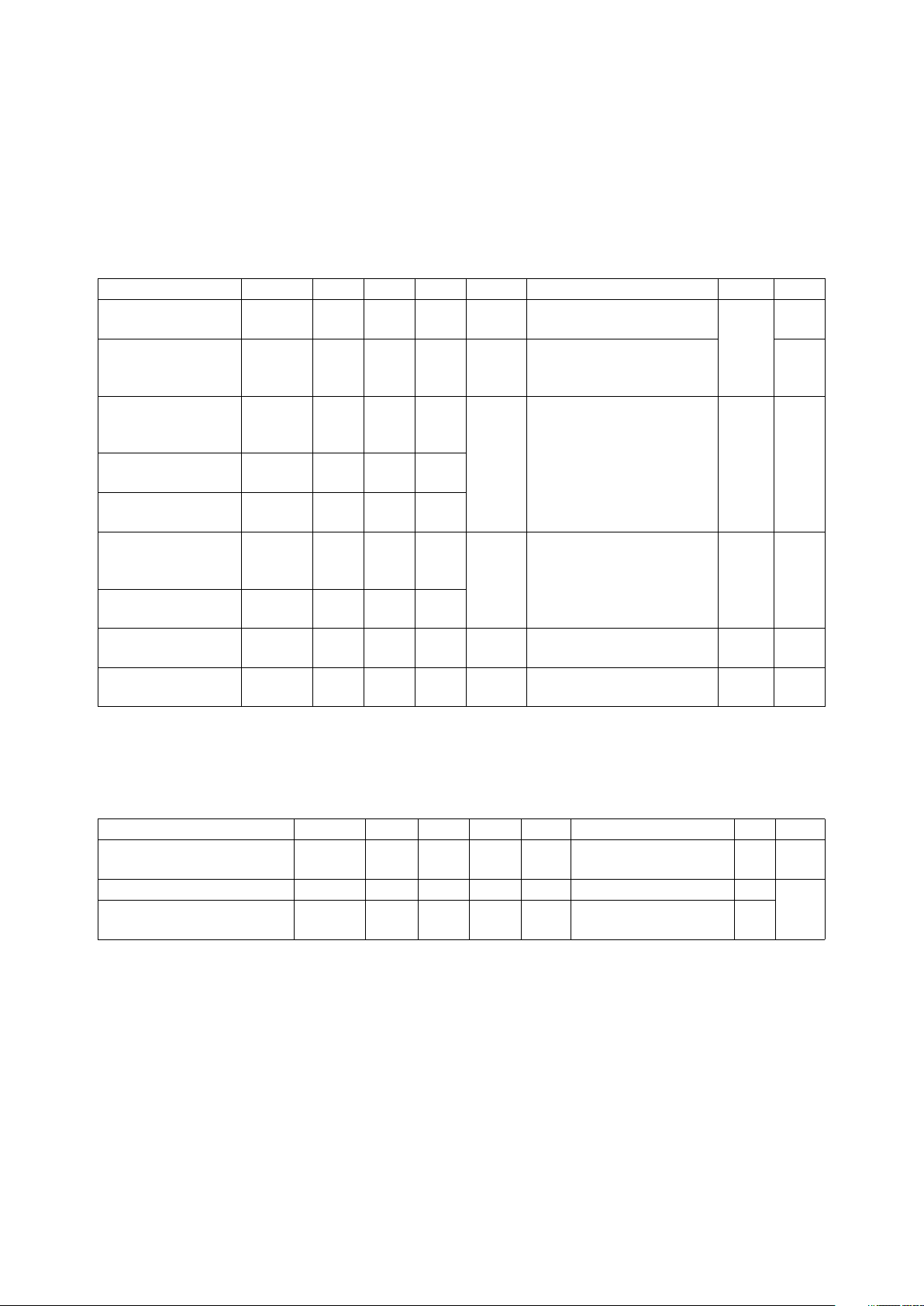
Figure 1. Input Offset Voltage Test Circuit.
Figure 2. Input Offset Change vs.
Temperature.
Figure 3. Input Offset Change vs.
V
DD1
and V
DD2
.
∆V
OS
– INPUT OFFSET CHANGE – mV
VDD – SUPPLY VOLTAGE – V
0.2
0.1
4.6
0.3
4.8 5.0 5.2
TA = 25°C
-0.1
vs. V
DD1 (VDD2
= 5 V)
4.4 5.65.4
vs. V
DD2 (VDD1
= 5 V)
0
∆V
OS
– INPUT OFFSET CHANGE – mV
TA – TEMPERATURE – °C
0
-0.2
-0.6
-20
0.6
20 60
V
DD1
= 5 V
V
DD2
= 5 V
-0.8
0.2
0.4
-40 100
-0.4
04080
Notes:
1. If V
IN-
is brought above V
DD1
- 2 V
with respect to GND1 an internal test
mode may be activated. This test
mode is not intended for customer
use.
2. Exact offset value is dependent on
layout of external bypass capacitors.
The offset value in the data sheet
corresponds to HP’s recommended
layout (see Figures 25 and 26).
3. Nonlinearity is defined as half of the
peak-to-peak output deviation from
the best-fit gain line, expressed as a
percentage of the full-scale differential output voltage.
4. Because of the switched capacitor
nature of the sigma-delta A/D
converter, time-averaged values are
shown.
5. CMRRIN is defined as the ratio of the
gain for differential inputs applied
between pins 2 and 3 to the gain for
common mode inputs applied to both
pins 2 and 3 with respect to pin 4.
6. When the differential input signal
exceeds approximately 320 mV, the
outputs will limit at the typical values
shown.
7. Short-circuit current is the amount of
output current generated when either
output is shorted to V
DD2
or ground.
HP does not recommend operation
under these conditions.
8. CMR (also known as IMR or Isolation
Mode Rejection) specifies the
minimum rate of rise of a common
mode noise signal applied across the
isolation boundary at which small
output perturbations begin to appear.
These output perturbations can occur
with both the rising and falling edges
of the common mode waveform and
may be of either polarity. A CMR
failure is defined as a perturbation
exceeding 200 mV at the output of
the recommended application circuit
(Figure 23). See applications section
for more information on CMR.
9. CMRR is defined as the ratio of
differential signal gain (signal applied
differentially between pins 2 and 3)
to the common mode gain (input pins
tied to pin 4 and the signal applied
between the input and the output of
the isolation amplifier) at 60 Hz,
expressed in dB.
10. Output noise comes from two primary
sources: chopper noise and sigma-
delta quantization noise. Chopper
noise results from chopper stabilization of the output op-amps. It occurs
at a specific frequency (typically 500
kHz) and is not attenuated by the onchip output filter. The on-chip filter
does eliminate most, but not all, of
the sigma-delta quantization noise.
An external filter circuit may be
easily added to the external postamplifier to reduce the total RMS
output noise. See applications section
for more information.
11. Data sheet value is the amplitude of
the transient at the differential output
of the HCPL-7840 when a 1 V
P-P
,
1 MHz square wave with 100 ns rise
and fall times (measured at pins 1
and 8) is applied to both V
DD1
and
V
DD2
.
12. In accordance with UL1577, each
isolation amplifer is proof tested by
applying an insulation test voltage
≥ 3000 V
RMS
for 1 second (leakage
current detection limit I
I-O
≤ 5 µA).
13. Device considered a two terminal
device: Pins 1, 2, 3 and 4 connected
together; pins 5, 6, 7 and 8
connected together.
0.1 µF
V
DD2
V
OUT
8
7
6
1
3
HCPL-7840
5
2
4
0.1 µF
10 K
10 K
V
DD1
+15 V
0.1 µF
0.1 µF
-15 V
+
–
AD624CD
GAIN = 100
0.47
µF
0.47
µF
Figure 4. Output Voltages vs. Input
Voltage.
V
O
– OUTPUT VOLTAGE – V
VIN – INPUT VOLTAGE – V
2.5
2.0
1.5
-0.4
4.0
-0.2 0 0.2
V
DD1
= 5 V
V
DD2
= 5 V
T
A
= 25°C
1.0
3.0
3.5
-0.6 0.60.4
POSITIVE
OUTPUT
NEGATIVE
OUTPUT
1-254
0.1 µF
V
DD2
8
7
6
1
3
HCPL-7840
5
2
4
0.01 µF
10 K
10 K
+15 V
0.1 µF
0.1 µF
-15 V
+
–
AD624CD
GAIN = 4
0.47
µF
0.47
µF
V
DD1
13.2
404
V
IN
V
OUT
+15 V
0.1 µF
0.1 µF
-15 V
+
–
AD624CD
GAIN = 10
10 K
0.47
µF
0.1 µF
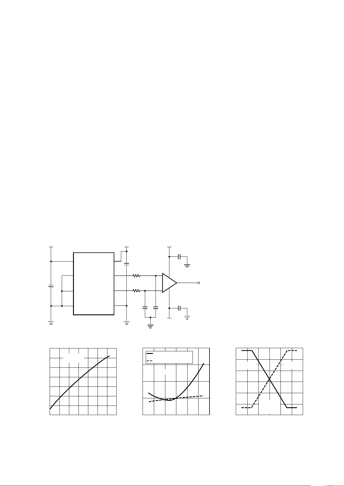
Figure 6. Gain Change vs.
Temperature.
Figure 5. Gain and Nonlinearity Test Circuit.
Figure 7. Gain Change vs. V
DD1
and
V
DD2
.
Figure 8. Nonlinearity Error Plot vs.
Input Voltage.
∆G
– GAIN CHANGE – %
TA – TEMPERATURE – °C
0
-0.3
-20
0.1
20 60
V
DD1
= 5 V
V
DD2
= 5 V
-0.5
-40 100
-0.1
04080
-0.2
-0.4
∆G – GAIN CHANGE – %
VDD – SUPPLY VOLTAGE – V
0.04
0.02
4.6
0.10
4.8 5.0 5.2
TA = 25°C
-0.06
0.06
vs. V
DD1 (VDD2
= 5 V)
0.08
4.4 5.65.4
vs. V
DD2 (VDD1
= 5 V)
0
-0.02
-0.04
NL ERROR – % OF FULL SCALE
V
IN+
– INPUT VOLTAGE – V
-0.05
-0.1
0.15
0 0.1
-0.10
0.05
200 mV ERROR
0.10
-0.2 0.2
100 mV ERROR
V
DD1
= 5 V
V
DD2
= 5 V
V
IN–
= 0 V
T
A
= 25°C
0
Figure 9. Nonlinearity vs.
Temperature.
Fibure 10. 200 mV Nonlinearity vs.
V
DD1
and V
DD2
.
Figure 11. 100 mV Nonlinearity vs.
V
DD1
and V
DD2
.
NL – NONLINEARITY – %
TA – TEMPERATURE – °C
0.10
0.05
0
0.20
20 60
0
0.15
200 mV NL
-40 100
100 mV NL
V
DD1
= 5 V
V
DD2
= 5 V
V
IN–
= 0 V
T
A
= 25 °C
-20 40 80
NL – NONLINEARITY – %
VDD – SUPPLY VOLTAGE – V
0.10
0.09
4.6
0.12
4.8 5.0 5.2
TA = 25°C
0.08
vs. V
DD1 (VDD2
= 5 V)
0.11
4.4 5.65.4
vs. V
DD2 (VDD1
= 5 V)
NL – NONLINEARITY – %
VDD – SUPPLY VOLTAGE – V
0.050
0.045
4.6
0.060
4.8 5.0 5.2
TA = 25°C
0.040
vs. V
DD1 (VDD2
= 5 V)
0.055
4.4 5.65.4
vs. V
DD2 (VDD1
= 5 V)

1-255
Figure 16. Common Mode Rejection
Test Circuit.
Figure 15. Output Supply Current vs.
Input Voltage.
Figure 18. Propagation Delays and
Rise/Fall Time vs. Temperature.
Figure 17. Propagation Delay, Rise/Fall Time and Bandwidth Test Circuit.
I
IN
– INPUT CURRENT – mA
V
IN+
– INPUT VOLTAGE – V
-4
-6
-8
-42-2 0 2
V
DD1
= 5 V
V
DD2
= 5 V
V
IN–
= 0 V
T
A
= 25°C
-10
-2
0
-6 64
NL – NONLINEARITY – %
FS – FULL-SCALE INPUT VOLTAGE – V
0.50
5.00
±0.10 ±0.20
V
DD1
= 5 V
V
DD2
= 5 V
0.01
TA = 85°C
0 ±0.40
T
A
= -40°C
0.05
TA = 25°C
±0.30
I
DD1
– INPUT SUPPLY CURRENT – mA
V
IN+
– INPUT VOLTAGE – V
9
11
-0.2 0
V
DD1
= 5 V
V
DD2
= 5 V
V
IN–
= 0 V
6
TA = 85°C
-0.4 0.40.2
T
A
= -40°C
TA = 25°C
10
8
7
Figure 12. Nonlinearity vs. Full-Scale
Input Voltage.
Figure 13. Input Current vs. Input
Voltage.
Figure 14. Input Supply Current vs.
Input Voltage.
I
DD2
– OUTPUT SUPPLY CURRENT – mA
V
IN+
– INPUT VOLTAGE – V
10.0
-0.2 0
V
DD1
= 5 V
V
DD2
= 5 V
V
IN–
= 0 V
8.0
TA = 85°C
-0.4 0.40.2
T
A
= -40°C
9.0
TA = 25°C
9.5
8.5
0.1 µF
V
DD2
V
OUT
8
7
6
1
3
HCPL-7840
5
2
4
2 K
2 K
78L05
+15 V
0.1 µF
0.1 µF
-15 V
–
+
MC34081
150
pF
IN OUT
0.1
µF
0.1
µF
9 V
PULSE GEN.
V
CM
+
–
10 K
10 K
150 pF
t – TIME – µs
TA – TEMPERATURE – °C
9
-20 0
2
DELAY TO 90%
-40 10020
RISE/FALL TIME
6
DELAY TO 50%
7
4
40 60 80
V
IN–
= 0 V
V
IN+
= 0 TO 100 mV STEP
V
DD1
= 5 V
V
DD2
= 5 V
3
5
8
0.1 µF
V
DD2
V
OUT
8
7
6
1
3
HCPL-7840
5
2
4
2 K
2 K
+15 V
0.1 µF
0.1 µF
-15 V
–
+
MC34081
0.1 µF
10 K
10 K
0.01 µF
V
DD1
V
IN
VIN IMPEDANCE LESS THAN 10 Ω.

1-256
Applications Information
Functional Description
Figure 22 shows the primary
functional blocks of the HCPL-
7840. In operation, the sigmadelta modulator converts the
analog input signal into a highspeed serial bit stream. The time
average of this bit stream is
directly proportional to the input
signal. This stream of digital data
is encoded and optically transmitted to the detector circuit. The
detected signal is decoded and
converted back into an analog
signal, which is filtered to obtain
the final output signal.
Application Circuit
The recommended application
circuit is shown in Figure 23. A
floating power supply (which in
many applications could be the
same supply that is used to drive
the high-side power transistor) is
regulated to 5 V using a simple
three-terminal voltage regulator
(U1). The voltage from the current sensing resistor, or shunt
(Rsense), is applied to the input
of the HCPL-7840 through an RC
anti-aliasing filter (R5, C3). And
finally, the differential output of
the isolation amplifier is
converted to a ground-referenced
single-ended output voltage with
a simple differential amplifier
circuit (U3 and associated components). Although the application circuit is relatively simple, a
few recommendations should be
followed to ensure optimal
performance.
Supplies and Bypassing
As mentioned above, an inexpensive 78L05 three-terminal
regulator can be used to reduce
the gate-drive power supply
voltage to 5 V. To help attenuate
high frequency power supply
noise or ripple, a resistor or
inductor can be used in series
with the input of the regulator to
form a low-pass filter with the
regulator’s input bypass
capacitor.
As shown in Figure 23, 0.1 µF
bypass capacitors (C2, C4)
should be located as close as
possible to the input and output
power supply pins of the HCPL-
7840. The bypass capacitors are
required because of the highspeed digital nature of the signals
inside the isolation amplifier. A
0.01 µF bypass capacitor (C3) is
also recommended at the input
pin(s) due to the switchedcapacitor nature of the input
circuit. The input bypass capacitor should be at least 1000 pF to
maintain gain accuracy of the
isolation amplifier.
Inductive coupling between the
input power-supply bypass
capacitor and the input circuit,
including the input bypass
capacitor and the input leads of
the HCPL-7840, can introduce
additional DC offset in the circuit.
Several steps can be taken to
minimize the mutual coupling
between the two parts of the
circuit, thereby improving the
offset performance of the design.
Separate the two bypass
capacitors C2 and C3 as much as
possible (even putting them on
opposite sides of the PC board),
while keeping the total lead
lengths, including traces, of each
bypass capacitor less than 20
mm. PC board traces should be
made as short as possible and
RELATIVE AMPLITUDE – dB
f – FREQUENCY – kHz
0
5
-4
1 50010
-2
-1
-3
50 100
V
DD1
= 5 V
V
DD2
= 5 V
T
A
= 25 °C
Figure 19. Amplitude Response vs.
Frequency.
Figure 20. 3 dB Bandwidth vs.
Temperature
Figure 21. RMS Input-Referred Noise
vs. Recommended Application Circuit
Bandwidth.
f (-3 dB) – 3 dB BANDWIDTH – kHz
TA – TEMPERATURE – °C
160
-20 0
40
-40 10020
100
140
80
40 60 80
120
60
V
DD1
= 5 V
V
DD2
= 5 V
V
N
– RMS INPUT-REFERRED NOISE – mV
f – FREQUENCY – KHz
2.5
10
0
V
IN+
= 200 mV
5 50050
V
IN+
= 0 mV
V
IN+
= 100 mV
2.0
0.5
100
TA = 25°C
V
DD1
= 5 V
V
DD2
= 5 V
1.5
1.0

1-257
placed close together or over
ground plane to minimize loop
area and pickup of stray magnetic
fields. Avoid using sockets, as
they will typically increase both
loop area and inductance. And
finally, using capacitors with
small body size and orienting
them perpendicular to each other
on the PC board can also help.
For more information concerning
this effect, see Application Note
1078, Designing with Hewlett-
Packard Isolation Amplifiers.
Shunt Resistor Selection
The current-sensing shunt resistor should have low resistance (to
minimize power dissipation), low
inductance (to minimize di/dt
induced voltage spikes which
could adversely affect operation),
and reasonable tolerance (to
maintain overall circuit accuracy).
The value of the shunt should be
chosen as a compromise between
minimizing power dissipation by
making the shunt resistance
smaller and improving circuit
accuracy by making it larger and
utilizing the full input range of
the HCPL-7840. Hewlett-Packard
recommends four different shunts
which can be used to sense
average currents in motor drives
up to 35 A and 35 hp. Table 1
shows the maximum current and
horsepower range for each of the
LVR-series shunts from Dale.
Even higher currents can be
sensed with lower value shunts
available from vendors such as
Dale, IRC, and Isotek (Isabellenhuette). When sensing currents
large enough to cause significant
heating of the shunt, the temperature coefficient of the shunt can
introduce nonlinearity due to the
signal dependent temperature
rise of the shunt. Using a heat
sink for the shunt or using a
shunt with a lower tempco can
help minimize this effect. The
Application Note 1078, Design-
ing with Hewlett-Packard
Isolation Amplifiers, contains
additional information on
designing with current shunts.
The recommended method for
connecting the isolation amplifier
to the shunt resistor is shown in
Figure 23. Pin 2 (V
IN+
) is connected to the positive terminal of
the shunt resistor, while pin 3
(V
IN-
) is shorted to pin 4 (GND1),
with the power-supply return
path functioning as the sense line
to the negative terminal of the
current shunt. This allows a
single pair of wires or PC board
traces to connect the isolation
amplifier circuit to the shunt
resistor. In some applications,
however, supply currents flowing
through the power-supply return
path may cause offset or noise
problems. In this case, better
performance may be obtained by
connecting pin 3 to the negative
terminal of the shunt resistor
separate from the power supply
return path. When connected this
way, both input pins should be
bypassed. Whether two or three
wires are used, it is recommended that twisted-pair wire or
very close PC board traces be
used to connect the current shunt
to the isolation amplifier circuit
to minimize electromagnetic
interference to the sense signal.
The 68 Ω resistor in series with
the input lead forms a low-pass
anti-aliasing filter with the input
bypass capacitor with a 200 kHz
bandwidth. The resistor performs
another important function as
well; it dampens any ringing
which might be present in the
circuit formed by the shunt, the
input bypass capacitor, and the
wires or traces connecting the
two. Undamped ringing of the
input circuit near the input
sampling frequency can alias into
the baseband producing what
might appear to be noise at the
output of the device. To be
effective, the damping resistor
should be at least 39 Ω.
PC Board Layout
In addition to affecting offset, the
layout of the PC board can also
affect the common mode rejection (CMR) performance of the
isolation amplifier, due primarily
to stray capacitive coupling
between the input and the output
circuits. To obtain optimal CMR
performance, the layout of the
printed circuit board (PCB)
should minimize any stray coupling by maintaining the maximum
possible distance between the
input and output sides of the
circuit and ensuring that any
ground plane on the PCB does
not pass directly below the
HCPL-7840. Using surface mount
components can help achieve
many of the PCB objectives
discussed in the preceding paragraphs. An example through-hole
PCB layout illustrating some of
the more important layout
recommendations is shown in
Figures 25 and 26. See Application Note 1078, Designing with
Hewlett-Packard Isolation
Amplifiers, for more information
on PCB layout considerations.
Post-Amplifier Circuit
The recommended application
circuit (Figure 23) includes a
post-amplifier circuit that serves
three functions: to reference the
output signal to the desired level
(usually ground), to amplify the
signal to appropriate levels, and

1-258
to help filter output noise. The
particular op-amp used in the
post-amp is not critical; however,
it should have low enough offset
and high enough bandwidth and
slew rate so that it does not
adversely affect circuit performance. The offset of the op-amp
should be low relative to the output offset of the HCPL-7840, or
less than about 5 mV.
To maintain overall circuit bandwidth, the post-amplifier circuit
should have a bandwidth at least
twice the minimum bandwidth of
the isolation amplifier, or about
200 kHz. To obtain a bandwidth
of 200 kHz with a gain of 5, the
op-amp should have a gainbandwidth greater than 1 MHz.
The post-amplifier circuit
includes a pair of capacitors (C5
and C6) that form a single-pole
low-pass filter. These capacitors
allow the bandwidth of the postamp to be adjusted independently
of the gain and are useful for
reducing the output noise from
the isolation amplifier (doubling
the capacitor values halves the
circuit bandwidth). The component values shown in Figure 23
form a differential amplifier with
a gain of 5 and a cutoff frequency
of approximately 100 kHz and
were chosen as a compromise
between low noise and fast
response times. The overall
recommended application circuit
has a bandwidth of 66 kHz, a rise
time of 5.2 µs and delay to 90%
of 8.5 µs.
The gain-setting resistors in the
post-amp should have a tolerance
of 1% or better to ensure adequate
CMRR and gain tolerance for the
overall circuit. Resistor networks
with even better ratio tolerances
can be used which offer better
performance, as well as reducing
the total component count and
board space.
The post-amplifier circuit can be
easily modified to allow for
single-supply operation. Figure
24 shows a schematic for a post
amplifier for use in 5 V single
supply applications. One additional resistor is needed and the
gain is decreased to 1 to allow
circuit operation over the full
input voltage range. See Application Note 1078, Designing with
Hewlett-Packard Isolation
Amplifiers, for more information
on the post-amplifier circuit.
Other Information
As mentioned above, reducing the
bandwidth of the post amplifier
circuit reduces the amount of
output noise. Figure 21 shows
how the output noise changes as
a function of the post-amplifier
bandwidth. The post-amplifier
circuit exhibits a first-order lowpass filter characteristic. For the
same filter bandwidth, a higherorder filter can achieve even
better attenuation of modulation
noise due to the second-order
noise shaping of the sigma-delta
modulator. For more information
on the noise characteristics of the
HCPL-7840, see Application Note
1078, Designing with Hewlett-
Packard Isolation Amplifiers.
The HCPL-7840 can also be used
to isolate signals with amplitudes
larger than its recommended
input range through the use of a
resistive voltage divider at its
input. The only restrictions are
that the impedance of the divider
be relatively small (less than
1KΩ so that the input resistance
(480 KΩ ) and input bias current
(0.6 A) do not affect the accuracy
of the measurement. An input
bypass capacitor is still required,
although the 68 Ω series damping
resistor is not (the resistance of
the voltage divider provides the
same function). The low pass
filter formed by the divider
resistance and the input bypass
capacitor may limit the
achievable bandwidth.
Table 1. Current Shunt Summary
Maximum Maximum Maximum
Shunt Power Average Horsepower
Shunt Resistor Part Number Resistance Dissipation Current Range
LVR-3.05-1% 50 mΩ 3 W 3 A 0.8-3.0 hp
LVR-3.02-1% 20 mΩ 3 W 8 A 2.2-8.0 hp
LVR-3.01-1% 10 mΩ 3 W 15 A 4.1-15 hp
LVR-5.005-1% 5 mΩ 5 W 35 A 9.6-35 hp

1-259
VOLTAGE
REGULATOR
CLOCK
GENERATOR
Σ∆
MODULATOR
ENCODER
LED DRIVE
CIRCUIT
DETECTOR
CIRCUIT
DECODER
AND D/A
FILTER
ISO-AMP
OUTPUT
VOLTAGE
REGULATOR
ISO-AMP
INPUT
ISOLATION
BOUNDARY
Figure 22. HCPL-7840 Block Diagram.
0.1 µF
+5 V
V
OUT
8
7
6
1
3
U2
5
2
4
R1
2.00 K
+15 V
C8
0.1 µF
0.1 µF
-15 V
–
+
MC34081
R3
10.0 K
HCPL-7840
C4
R4
10.0 K
C6
150 pF
U3
U1
78L05
IN OUT
C1
C2
0.01
µF
R5
68
GATE DRIVE
CIRCUIT
POSITIVE
FLOATING
SUPPLY
• • •
HV+
• • •
HV–
• • •
–+
R
SENSE
MOTOR
C5
150 pF
0.1
µF
0.1
µF
C3
C7
R2
2.00 K
Figure 26. Bottom Layer of Printed
Circuit Board Layout.
TO R
SENSE+
TO R
SENSE–
TO V
DD1
TO V
DD2
V
OUT+
V
OUT–
Figure 25. Top Layer of Printed
Circuit Board Layout.
C3
C2
C4
R5
Figure 24. Single-Supply Post-Amplifier Circuit.
0.1 µF
+5 V
V
OUT
8
7
6
1
3
U2
5
2
4
R1
10.0 K
+5 V
C8
0.1 µF
–
+
MC34071
R3
10.0 K
HCPL-7840
C4
R4B
20.0 K
C6
150 pF
U3
R4A
20.0 K
+5 V
C5
150 pF
R2
10.0 K
Figure 23. Recommended Application Circuit.
 Loading...