

查询HMC311ST89供应商
MICROWAVE CORPORATION
Typical Applications
8
The HMC311ST89 is an ideal RF/IF gain block
or LO buffer amplifi er for:
• Cellular / PCS / 3G
• Fixed Wireless & WLAN
• CATV & Cable Modem
• Microwave Radio
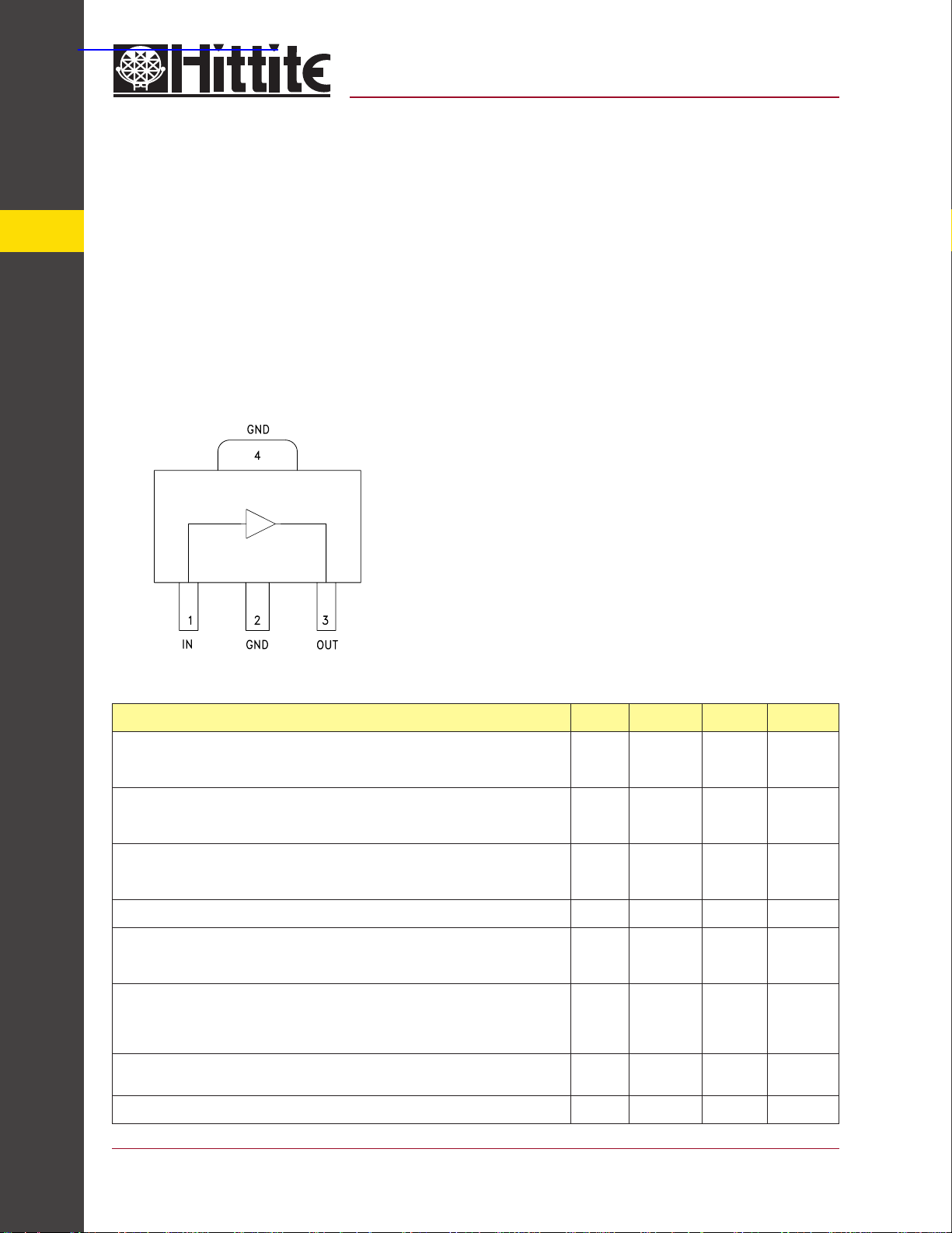
Functional Diagram
AMPLIFIERS - SMT
v00.0204
HMC311ST89
InGaP HBT GAIN BLOCK
MMIC AMPLIFIER, DC - 6.0 GHz
Features
P1dB Output Power: +15.5 dBm
Output IP3: +31.5 dBm
Gain: 16 dB
50 Ohm I/O’s
Industry Standard SOT89 Package
General Description
The HMC311ST89 is a GaAs InGaP Heterojunction
Bipolar Transistor (HBT) Gain Block MMIC SMT
DC to 6 GHz amplifi er. Packaged in an industry
standard SOT89, the amplifi er can be used as
either a cascadable 50 Ohm gain stage or to drive
the LO of HMC mixers with up to +16.5 dBm output
power. The HMC311ST89 offers 16 dB of gain
and an output IP3 of +31.5 dBm while requiring
only 54 mA from a +5V supply. The Darlington
feedback pair used results in reduced sensitivity
to normal process variations and yields excellent
gain stability over temperature while requiring a
minimal number of external bias components.
Electrical Specifi cations, Vs= 5.0 V, Rbias= 22 Ohm, T
Parameter Min. Typ. Max. Units
Gain
Gain Variation Over Temperature DC - 2.0 GHz
Return Loss Input / Output
Reverse Isolation DC - 6.0 GHz 20 dB
Output Power for 1 dB Compression (P1dB) DC - 2.0 GHz
Output Third Order Intercept (IP3)
Noise Figure
Supply Current (Icq) 54 mA
Note: Data taken with broadband bias tee on device output.
DC - 1.0 GHz
1.0 - 4.0 GHz
4.0 - 6.0 GHz
2.0 - 4.0 GHz
4.0 - 6.0 GHz
DC - 2.0 GHz
2.0 - 5.0 GHz
5.0 - 6.0 GHz
2.0 - 4.0 GHz
4.0 - 6.0 GHz
DC - 1.0 GHz
1.0 - 2.0 GHz
2.0 - 4.0 GHz
4.0 - 6.0 GHz
DC - 4.0 GHz
4.0 - 6.0 GHz
= +25° C
A
14.0
13.0
12.5
13.5
12.0
10.0
16.0
15.0
14.5
0.004
0.007
0.012
8
7
8
15.5
15.0
13.0
31.5
30
27
24
4.5
5
0.007
0.012
0.016
dB
dB
dB
dB/ °C
dB/ °C
dB/ °C
dB
dB
dB
dBm
dBm
dBm
dBm
dBm
dBm
dBm
dB
8 - 74
For price, delivery, and to place orders, please contact Hittite Microwave Corporation:
12 Elizabeth Drive, Chelmsford, MA 01824 Phone: 978-250-3343 Fax: 978-250-3373
Order Online at www.hittite.com
MICROWAVE CORPORATION
v00.0204
HMC311ST89
InGaP HBT GAIN BLOCK
MMIC AMPLIFIER, DC - 6.0 GHz
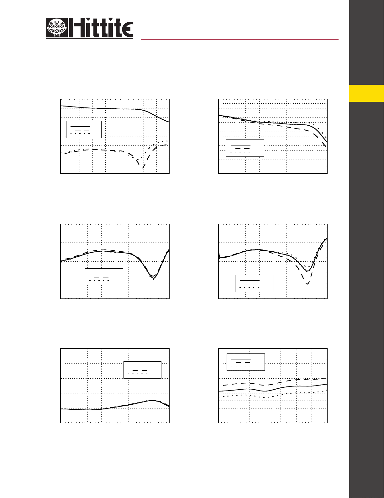
Broadband Gain & Return Loss Gain vs. Temperature
20
15
10
5
0
-5
RESPONSE (dB)
-10
-15
-20
123456789
S21
S11
S22
FREQUENCY (GHz)
Input Return Loss vs. Temperature
0
-5
20
19
18
17
16
15
14
13
12
11
GAIN (dB)
10
9
8
7
6
5
4
012345678
+25C
+85C
-40C
FREQUENCY (GHz)
Output Return Loss vs. Temperature
0
-5
8
AMPLIFIERS - SMT
-10
+25C
-15
INPUT RETURN LOSS (dB)
-20
012345678
+85C
-40C
FREQUENCY (GHz)
Reverse Isolation vs. Temperature
0
-5
-10
-15
-20
REVERSE ISOLATION (dB)
-25
012345678
FREQUENCY (GHz)
+25C
+85C
-40C
-10
-15
OUTPUT RETURN LOSS (dB)
-20
012345678
+25C
+85C
-40C
FREQUENCY (GHz)
Noise Figure vs. Temperature
10
9
8
7
6
5
4
3
NOISE FIGURE (dB)
2
1
0
12345678
+25C
+85C
-40C
FREQUENCY (GHz)
For price, delivery, and to place orders, please contact Hittite Microwave Corporation:
12 Elizabeth Drive, Chelmsford, MA 01824 Phone: 978-250-3343 Fax: 978-250-3373
Order Online at www.hittite.com
8 - 75

MICROWAVE CORPORATION
v00.0204
HMC311ST89
InGaP HBT GAIN BLOCK
P1dB vs. Temperature Psat vs. Temperature
8
18
16
14
12
10
P1dB (dBm)
8
6
4
012345678
FREQUENCY (GHz)
Power Compression @ 1 GHz
AMPLIFIERS - SMT
18
16
14
12
10
8
6
4
2
0
Pout (dBm), GAIN (dB), PAE (%)
-2
-4
-20 -18 -16 -14 -12 -10 -8 -6 -4 -2 0 2 4 6
INPUT POWER (dBm)
+25C
+85C
-40C
Pout
Gain
PAE
MMIC AMPLIFIER, DC - 6.0 GHz
18
16
14
12
10
Psat (dBm)
8
6
4
012345678
Power Compression @ 6 GHz
18
16
14
12
10
8
6
4
2
0
Pout (dBm), GAIN (dB), PAE (%)
-2
-4
-20 -18 -16 -14 -12 -10 -8 -6 -4 -2 0 2 4 6
+25C
+85C
-40C
FREQUENCY (GHz)
INPUT POWER (dBm)
Pout
Gain
PAE
8 - 76
Output IP3 vs. Temperature
34
32
30
28
26
24
22
20
OIP3 (dBm)
18
16
14
12
10
012345678
For price, delivery, and to place orders, please contact Hittite Microwave Corporation:
12 Elizabeth Drive, Chelmsford, MA 01824 Phone: 978-250-3343 Fax: 978-250-3373
+25C
+85C
-40C
FREQUENCY (GHz)
Gain, Power, OIP3 & Supply Current vs.
Supply Voltage @ 1 GHz
40
35
30
25
20
15
10
5
GAIN (dB), P1dB (dBm), Psat (dBm), OIP3 (dBm)
4.5 4.75 5 5.25 5.5
Order Online at www.hittite.com
80
70
60
Icq (mA)
50
40
30
Gain
P1dB
20
Icq
Vs (Vdc)
Psat
OIP3
10

MICROWAVE CORPORATION
v00.0204
HMC311ST89
InGaP HBT GAIN BLOCK
Absolute Maximum Ratings
Collector Bias Voltage (Vcc) +7 Volts
RF Input Power (RFin)(Vcc = +3.9 Vdc) +10 dBm
Junction Temperature 150 °C
Continuous Pdiss (T = 85 °C)
(derate 5.21 mW/°C above 85 °C)
Thermal Resistance
(junction to lead)
Storage Temperature -65 to +150 °C
Operating Temperature -40 to +85 °C
0.34 W
191 °C/W
Outline Drawing
MMIC AMPLIFIER, DC - 6.0 GHz
8
AMPLIFIERS - SMT
NOTES:
1. MATERIAL PACKAGE BODY: LOW STRESS INJECTION MOLDED
PLASTIC SILICA AND SILICON IMPREGNATED.
2. LEAD AND GROUND PADDLE MATERIAL: COPPER ALLOY
3. LEAD AND GROUND PADDLE PLATING: Sn/Pb SOLDER
4. DIMENSIONS ARE IN INCHES [MILLIMETERS].
5. LEAD SPACING TOLERANCE IS NON-CUMULATIVE
6. PAD BURR LENGTH SHALL BE 0.15mm MAXIMUM.
PAD BURR HEIGHT SHALL BE 0.05mm MAXIMUM.
7. PACKAGE WARP SHALL NOT EXCEED 0.05mm.
8. ALL GROUND LEADS AND GROUND PADDLE MUST BE SOLDERED
TO PCB RF GROUND.
For price, delivery, and to place orders, please contact Hittite Microwave Corporation:
12 Elizabeth Drive, Chelmsford, MA 01824 Phone: 978-250-3343 Fax: 978-250-3373
Order Online at www.hittite.com
8 - 77

MICROWAVE CORPORATION
v00.0204
HMC311ST89
InGaP HBT GAIN BLOCK
Pin Descriptions
8
Pin Number Function Description Interface Schematic
1 RFIN
3 RFOUT
2, 4 GND
AMPLIFIERS - SMT
Application Circuit
MMIC AMPLIFIER, DC - 6.0 GHz
This pin is DC coupled.
An off chip DC blocking capacitor is required.
RF output and DC Bias for the output stage.
These pins and package bottom must be connected to
RF/DC ground.
Note:
1. Select Rbias to achieve Icq using equation below,
Rbias
2. External blocking capacitors are required on
RFIN and RFOUT.
>
22 Ohm.
Icq = Vs - 3.9
Rbias
Recommended Component Values
Component
L1 270 nH 56 nH 18 nH 18 nH 15 nH 8.2 nH 3.3 nH 3.3 nH
C1, C2 0.01 µF 100 pF 100 pF 100 pF 100 pF 100 pF 100 pF 100 pF
50 900 1900 2200 2400 3500 5200 5800
Frequency (MHz)
8 - 78
For price, delivery, and to place orders, please contact Hittite Microwave Corporation:
12 Elizabeth Drive, Chelmsford, MA 01824 Phone: 978-250-3343 Fax: 978-250-3373
Order Online at www.hittite.com

MICROWAVE CORPORATION
v00.0204
HMC311ST89
InGaP HBT GAIN BLOCK
Evaluation PCB
MMIC AMPLIFIER, DC - 6.0 GHz
8
AMPLIFIERS - SMT
List of Materials for Evaluation PCB 108313*
Item Description
J1 - J2 PC Mount SMA Connector
J3 - J4 DC Pin
C1, C2 Capacitor, 0402 Pkg.
C3 100 pF Capacitor, 0402 Pkg.
C4 1000 pF Capacitor, 0603 Pkg.
C5 2.2 µF Capacitor, Tantalum
R1 Resistor, 0805 Pkg.
L1 Inductor, 0603 Pkg.
U1 HMC311ST89
PCB** 107368 Evaluation PCB
** Circuit Board Material: Rogers 4350
* Reference this number when ordering complete evaluation PCB.
For price, delivery, and to place orders, please contact Hittite Microwave Corporation:
12 Elizabeth Drive, Chelmsford, MA 01824 Phone: 978-250-3343 Fax: 978-250-3373
Order Online at www.hittite.com
The circuit board used in the fi nal application should use
RF circuit design techniques. Signal lines should have
50 ohm impedance while the package ground leads and
package bottom should be connected directly to the
ground plane similar to that shown. A suffi cient number of
VIA holes should be used to connect the top and bottom
ground planes. The evaluation board should be mounted
to an appropriate heat sink. The evaluation circuit board
shown is available from Hittite upon request.
8 - 79
 Loading...