HA13164A
Multiple Voltage Regulator
ADE-207-342 (Z)
Rev.0
Jun. 2001
General Descrip tion
The HA13164A is a compact multiple voltage regulator for car audio system. The outputs of this IC output
consist of regulated 5.7 V output for a microcontroller, regulated 8 V output for CD driver, regulated 9.0 V
output for audio control, regulated 10 V output for illuminations and regulated 5 V output, VCC-dependent
output for external output and VCC-dependent output for remort-ANT.
Functions
General
• ACC power monitor circuit is built-in as to detect lo w voltage.
• Low saturation output (PNP output) used for audio output.
• Adjustable voltage for illumination output by changing an external resister.
P rotec tions
• Output current limit circuit to avoid device destruction caused by shorted output, etc.
• High surge input protector against VCC and ACC.
• Built in a thermal shutdown circuit to prevent against the thermal destruction.

HA13164A
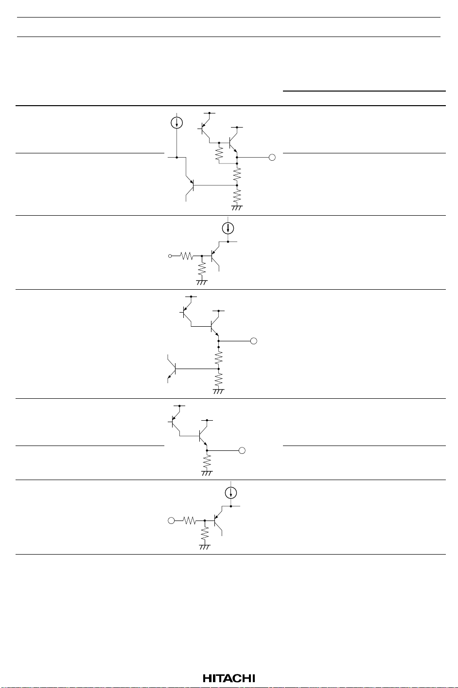
Pin Descrip tion a n d E quiv alent Ci rc ui t
FunctionPin
No. Pin Name Specification Equivalent Circuit
1 EXT OUT VCC-1V/300mA min Output voltage is
Vcc
Vcc
2 ANT OUT VCC-1V/300mA min
90kΩ
10kΩ
Normal Operation TSD Surge Input
VCC-1 V when M
or H level applied to
CTRL pin.
Output voltage is
VCC-1 V when M
or H level to CTRL
pin and H level to
ANT-CTRL.
0V 0V
0V 0V
3ACCIN —
Connected to ACC. — —
45kΩ
15kΩ
4 VDD OUT 5.7V/100mA min
Vcc
Regular 5.7V. 5.7V 0V
Vcc
175kΩ
50kΩ
5 SW5VOUT 5.0V/100mA min Output voltage is
6 COMPOUT 5.0V/100mA min
7 ANT CTRL —
VDD
Vcc
50kΩ
5V when M or H
level applied to
CTRL pin.
Output for ACC
detector
L: ANT output OFF
H: ANT output ON
51kΩ
0V 0V
0V 0V
——
Rev.0, Jun. 2001, page 2 of 18
49kΩ

HA13164A
Pin Descript io n an d Equivalent Circuit (cont)
FunctionPin
No. Pin Name Specification Equivalent Circuit
8 VCC — Connected to VCC — —
9 BATT DET —
250kΩ
VDD
10kΩ
Normal Operation TSD Surge Input
Low battery detect. Detect Not det ect
10 AUDIOOUT 9.0V/500mA min
11 CTRL —
12 CD OUT 8.0V/1.3A min
65kΩ
35kΩ
Vcc
Vcc
Vcc
64.7kΩ
12.4kΩ
Vcc
77.3kΩ
12.3kΩ
Output voltage is
9V when M or H
level applied to
CTRL pin.
L: BIAS OFF
M: BIAS ON
H: CD ON
Output voltage is
8V when H level
applied to CTRL
pin.
0V 0V
——
0V 0V
13 ILM AJ — Adjustment pin for
14 ILM OUT 9.85V/500mA min
Vcc
Vcc
33.4kΩ
ILM output voltage.
Output voltage is
10V when M or H
level applied to
CTRL pin
——
0V 0V
5kΩ
15 GND — Connected to GND — —
Rev.0, Jun. 2001, page 3 of 18

HA13164A
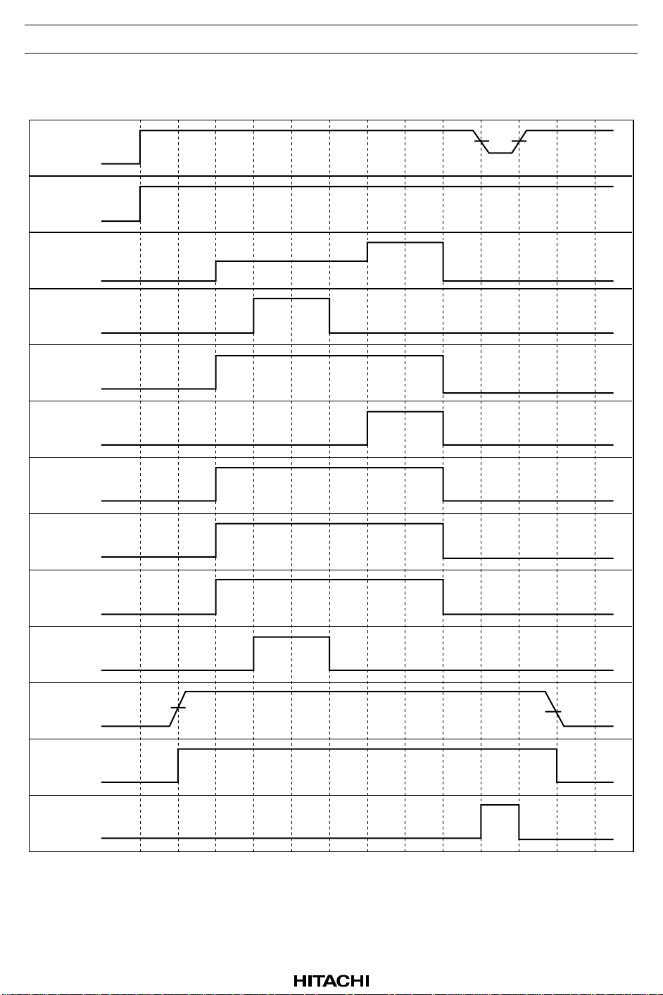
Timing Cha r t
VCC
VDD
CTRL
ANTCTRL
AUDIO
CD
ILM
EXT
9.25V8.5V
SW5V
ANT
ACC
COMP
B.DET current
Rev.0, Jun. 2001, page 4 of 18
2.8V
2.5V

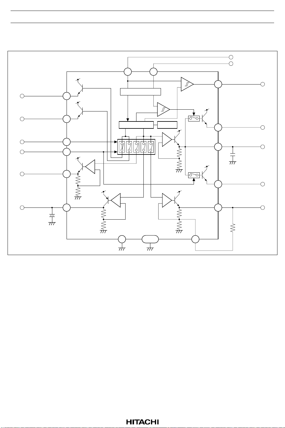
Block Diagram
ANT OUT
EXT OUT
ANT CTRL
CTRL
CC OUT
11
12
HA13164A
+B
BATT.DET
9
COMP OUT
6
VDD OUT
4
SW5V
5
ACC
VCC
8
2
1
7
+
−
Surge protector
BIAS TSD
ACC
3
+
−
+
−
+
−
AUDIO OUT
+
−
GND
15
+
TAB
GND
10 14
+
−
13
ILM AJ
ILM OUT
Rev.0, Jun. 2001, page 5 of 18

HA13164A
Absolute Maximu m R at i ngs
(Ta = 25°C)
Item Symbol Value Unit Note
Operating power supply voltage Vcc 18 V
DC supply voltage Vcc(DC) 26 V 1
Peak voltage Vcc(PEAK) 50 V 2
Power dissipation Pd 36 W 3
Junction temperature Tj 150 °C
Operating temperature Topr –40 to +85 °C
Storage temperature Tstg –55 to +125 °C
Notes: Recommended power supply voltage range 10V to 16V.
1. Applied time is less than 30 sec.
2. Surge pulse as input.
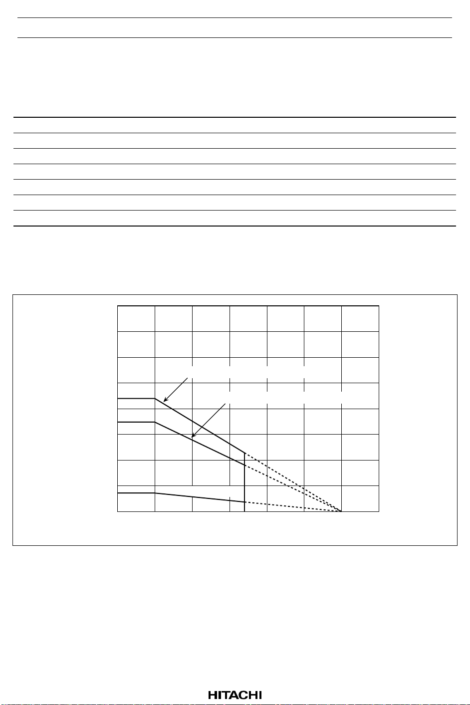
3. Ta=25°C. :Permissible power dissipation when using a heat sink of infinite area. Refer to the
derating curves below.
20
15
thin = 1.6mm, 100cm2 Aluminum heat sink
11.0W
10
8.7W
Power dissipation Pd (W)
5
1.8W
0
0 50 1007525
thin = 1.6mm, 50cm2 Aluminum heat sink
w/o heat sink
150125 175
Ambient temperature Ta (°C)
Rev.0, Jun. 2001, page 6 of 18
 Loading...