


HA13705C
IPIC (Intelligent Power IC) High Side Solenoid Driver
ADE-207-207 (Z)
1st Edition
July 1996
Description
The HA13705C is high side power driver IC with protectors and diagnostic function. The device is especially
designed to switch inductive loads.
Functions
• Power MOS source follower output (2 A)
• With Over Voltage Shut Down circuit (OVSD)
• With Over Current protector circuit (OCSD)
• With Over Temperature Shut Down circuit (OTSD)
• With diagnostic circuit and status output
• With fail safe function under input open circuit condition
• With low voltage inhibit circuit (LVI)
• With output negative voltage clamp circuit
Features
• Protected against 60 V load dump condition
• Low RON (0.17 Ω Typ)
• Wide operating supply voltage range (VDD = 7 V to 25 V)
• High sustaining voltage (–25 V)
• Protected against reverse supply voltage (–13 V)
• Protected against short circuit condition
• Input compatible with TTL, LS-TTL, or 5 V CMOS
HA13705C
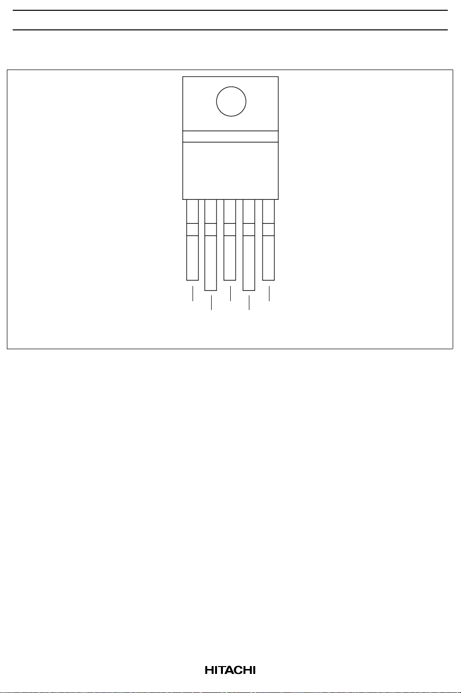
Pin Arrangement
HA13705C
12345
V
GND OUT
DD
STATUSINPUT
(Top View)
2
Block Diagram
HA13705C
V
DD
3
INPUT
2
STATUS
4
LVI
Logic
Charge
Pump
TSD
160
175
1
OVSD
OSC. Latch
Band
Gap
Ref.
Diagnostic
Voltage
Clamp
Current
Sense
+
—
Vref
Open, Short to
Detector
V
DD
OUT
5
3
GND

HA13705C
Truth Table
Mode In Out Status
Normal L L L
HHH
Load short L L L
HL L
Load open L H H
HHH
Short to V
OTSD
OVSD
LVI
DD
*1
*2
*3
L : Low level (0.8 V)
H : High level (2.0 V)
Notes: 1. OTSD: Over temperature shut down
2. OVSD: Over voltage shut down
3. LVI: Low voltage inhhibit
LHH
HHH
LLL
HL L
LLH
HL H
LLH
HL H
4

Absolute Maximum Ratings (Ta = 25°C)
Item Symbol Rating Unit Notes
Continuous supply voltage V
Transient supply voltage V
Input voltage V
DD
DD
IN
Output voltage Vout –25 to V
Status voltage Vs –0.3 to +15 V
Output current Iout — A 3, 4
Status current Is 5 mA
Power dissipation P
Package thermal resistance/
T
θj–c 5 °C/W
Junction to case
Package thermal resistance/
θj–a 70 °C/W
Junction to air
Junction temperature range Tj –40 to 150 °C
Storage temperature range Tstg –55 to +150 °C
Notes: 1. Recommended operating voltage:
V
= 7 to 16 V (Normal)
DD
16 to 25 V (Jump up start 5 minutes MAX)
–13 V (Reverse Battely 5 minutes MAX)
2. Load dump condition
–13 to 35 V 1
60 V 2
–0.3 to 30 V
DD
V3
—W5
HA13705C
60 V
14 V
Tr
V = 14 + 46 e
Tr = 1ms
t
—
0.25
5

HA13705C
)
3. Output Transistor ASO (Reference Data)
I
(A)
D
10
7
10ms
1ms
5
Limited area
4
by over current
3
protection
2
1
0.5
0.1
2 5 10 20
30405060
VDS (V
4. Internally limited
5. Maximum power dissipation (P
P
(Max) = (Tjopr(Max) – Tambient) / (θj-c + θc-a)
T
(Max)) can be defined as:
T
θc-a: Thermal resistance between case and air (Depend on heat sink size)
6

HA13705C
Electrical Characteristics (Ta = 25°C, VCC = 12 V ±10%)
Item Symbol Min Typ Max Unit Test Conditions Pin Note
Output R (ON) R
DS(ON)
— 0.17 0.36 Ω IO = 2 A
(@Tj = –40 to 150°C)
Operating supply
V
DD
7—25V 3
voltage range
Quiescent current I
Output leakage current I
I
DD1
DD2
LEAK
— — 0.3 mA VIN = 0 V, Vout = 0 V 3
— 6.0 10.0 mA VIN = 5.5 V, Vout = open 3
— — 0.1 mA VDD = 25 V, VIN = 0 V,
Vout = 0 V
Input threshold voltage V
Input current I
Propagation delay time t
V
IL
I
IH
d(ON)
t
r
t
d(OFF)
IL
IH
— — 0.8 V 2
2.0 — — V 2
–10 — 60 µAVIN = 0.8 V 2
50 — 300 µAVIN = 5.0 V 2
——50µsIO = 1 A 2, 5
——90µs5
——50µs 2, 5
Tf ——50µs5
Open det. threshold
I
OD
2 10 100 µs 4, 5
current
Current limiter operating
I
CS
3.0 4.3 7.5 A 5
level
LVI operating level L.V.I — 5 6 V 3
Over
voltage
Operating
level
OVSD 26 29 33 V 3
shut
down
Hysteresis VHYS 0.15 0.5 1.5 V 3
Output sustain voltage V
Over
temper-
Operating
level
(SUS)
OTSD 150 175 — °C51
— — –25 V Iout = 20 mA 5
ature
shut
down
Hysteresis THYS — 15 — °C51
Status on voltage V
Status leakage current I
SL
S(Leak)
— — 0.4 V IS = 1 mA 4
–10 — 100 µAVS = 5.0 V 4
Notes: 1. Design parameter only (no test)
5
5
7

HA13705C
Solenoid Drive Application and it’s Waveform
V
DD
C1
3
STATUS
4
VCC (5 V)
R2
INPUT
INPUT
R1
2
HA13705C
OUTPUT
5
1
GND
R1 : Input series resistance to protect CMOS driver.
R2 : Pull up resistance at status output.
C1 : The capacitor to compensate the inductance at V
D1, DZ1 : for Reverse voltage clamp
Normal
5 V
0
I
CS
D1
DZ1
Output short
to GND
DD
line.
Iout
Vout
V (SUS)
STATUS
0
1.8 ms (Typ)
V
DD
0
V
CC
0
8

Package Dimensions
HA13705C
Unit: mm
17.0 ± 0.3
15.2 ± 0.3
1
1.7
3.4
10.0 ± 0.3
7.0 ± 0.3
5
φ
1 Max
3.2 ± 0.2
12.0 ± 0.3
0.5 Max
0.6
8.45
8.2
4.3
2.79 ± 0.15
2.5 ± 0.2
2.1 ± 0.2
4.44 ± 0.20
2.5 ± 0.2
20.6
21.9
Hitachi Code
JEDEC
EIAJ
Weight
(reference value)
SP-5TA
—
—
2.0 g
9

Cautions
1. Hitachi neither warrants nor grants licenses of any rights of Hitachi’s or any third party’s patent,
copyright, trademark, or other intellectual property rights for information contained in this document.
Hitachi bears no responsibility for problems that may arise with third party’s rights, including
intellectual property rights, in connection with use of the information contained in this document.
2. Products and product specifications may be subject to change without notice. Confirm that you have
received the latest product standards or specifications before final design, purchase or use.
3. Hitachi makes every attempt to ensure that its products are of high quality and reliability. However,
contact Hitachi’s sales office before using the product in an application that demands especially high
quality and reliability or where its failure or malfunction may directly threaten human life or cause risk
of bodily injury, such as aerospace, aeronautics, nuclear power, combustion control, transportation,
traffic, safety equipment or medical equipment for life support.
4. Design your application so that the product is used within the ranges guaranteed by Hitachi particularly
for maximum rating, operating supply voltage range, heat radiation characteristics, installation
conditions and other characteristics. Hitachi bears no responsibility for failure or damage when used
beyond the guaranteed ranges. Even within the guaranteed ranges, consider normally foreseeable
failure rates or failure modes in semiconductor devices and employ systemic measures such as failsafes, so that the equipment incorporating Hitachi product does not cause bodily injury, fire or other
consequential damage due to operation of the Hitachi product.
5. This product is not designed to be radiation resistant.
6. No one is permitted to reproduce or duplicate, in any form, the whole or part of this document without
written approval from Hitachi.
7. Contact Hitachi’s sales office for any questions regarding this document or Hitachi semiconductor
products.
Hitachi, Ltd.
Semiconductor & Integrated Circuits.
Nippon Bldg., 2-6-2, Ohte-machi, Chiyoda-ku, Tokyo 100-0004, Japan
Tel: Tokyo (03) 3270-2111 Fax: (03) 3270-5109
URL NorthAmerica : http:semiconductor.hitachi.com/
For further information write to:
Hitachi Semiconductor
(America) Inc.
179 East Tasman Drive,
San Jose,CA 95134
Tel: <1> (408) 433-1990
Fax: <1>(408) 433-0223
Europe : http://www.hitachi-eu.com/hel/ecg
Asia (Singapore) : http://www.has.hitachi.com.sg/grp3/sicd/index.htm
Asia (Taiwan) : http://www.hitachi.com.tw/E/Product/SICD_Frame.htm
Asia (HongKong) : http://www.hitachi.com.hk/eng/bo/grp3/index.htm
Japan : http://www.hitachi.co.jp/Sicd/indx.htm
Hitachi Europe GmbH
Electronic components Group
Dornacher Stra§e 3
D-85622 Feldkirchen, Munich
Germany
Tel: <49> (89) 9 9180-0
Fax: <49> (89) 9 29 30 00
Hitachi Europe Ltd.
Electronic Components Group.
Whitebrook Park
Lower Cookham Road
Maidenhead
Berkshire SL6 8YA, United Kingdom
Tel: <44> (1628) 585000
Fax: <44> (1628) 778322
Hitachi Asia Pte. Ltd.
16 Collyer Quay #20-00
Hitachi Tower
Singapore 049318
Tel: 535-2100
Fax: 535-1533
Hitachi Asia Ltd.
Taipei Branch Office
3F, Hung Kuo Building. No.167,
Tun-Hwa North Road, Taipei (105)
Tel: <886> (2) 2718-3666
Fax: <886> (2) 2718-8180
Copyright ' Hitachi, Ltd., 1999. All rights reserved. Printed in Japan.
Hitachi Asia (Hong Kong) Ltd.
Group III (Electronic Components)
7/F., North Tower, World Finance Centre,
Harbour City, Canton Road, Tsim Sha Tsui,
Kowloon, Hong Kong
Tel: <852> (2) 735 9218
Fax: <852> (2) 730 0281
Telex: 40815 HITEC HX
 Loading...