

Page 1
AVR 2550 Audio/VideoReceiver
AVR 2550
Service Manual
Power for the Digital Revolution
®
™
Page 2

TECHNICAL SPECIFICATIONS
Technical Specifications
Audio Section
Stereo Mode
Continuous Average Power (FTC)
50 Watts per channel, 20Hz–20kHz,
@ < 0.07% THD, both channels driven into 8 ohms
Five-Channel Surround Modes
Power Per Individual Channel
Front L&R channels:
40 Watts per channel,
@ < 0.07% THD, 20Hz–20kHz into 8 ohms
Center channel:
40 Watts, @ < 0.07% THD, 20Hz–20kHz into 8 ohms
Surround channels:
40 Watts per channel,
@ < 0.07% THD, 20Hz–20kHz into 8 ohms
Input Sensitivity/Impedance
Linear (High Level) 200mV/47kohms
Signal-to-Noise Ratio (IHF-A) 95dB
Surround System Adjacent Channel Separation
Analog Decoding 40dB
(Pro Logic, etc.)
Dolby Digital (AC-3) 55dB
DTS 55dB
Frequency Response
@ 1W (+0dB, –3dB) 10Hz–100kHz
High Instantaneous
Current Capability (HCC) ±25 Amps
Transient Intermodulation
Distortion (TIM) Unmeasurable
Rise Time 16 µsec
Slew Rate 40V/µsec
FM Tuner Section
Frequency Range 87.5–108MHz
Usable Sensitivity IHF 1.3 µV/13.2dBf
Signal-to-Noise Ratio Mono/Stereo: 70/65dB (DIN)
Distortion Mono/Stereo: 0.15/0.3%
Stereo Separation 35dB @ 1kHz
Selectivity ±300kHz: 65dB
Image Rejection 80dB
IF Rejection 90dB
AM Tuner Section
Frequency Range 522–1620kHz
Signal-to-Noise Ratio 45dB
Usable Sensitivity Loop: 500µV
Distortion 1kHz, 50% Mod: 0.8%
Selectivity ±9kHz: 30dB
Video Section
Video Format PAL/NTSC
Input Level/Impedance 1Vp-p/75 ohms
Output Level/Impedance 1Vp-p/75 ohms
Video Frequency
Response 10Hz–8MHz (–3dB)
General
Power Requirement AC 220-240V/50Hz
Power Consumption 72W idle, 580W maximum
(2 channels driven)
Dimensions (Max)
Width 440mm
Height 166mm
Depth 365mm
Weight 10.6 kg
Depth measurement includes knobs, buttons and terminal connections.
Height measurement includes feet and chassis.
All features and specifications are subject to change without notice.
Harman Kardon is a registered trademark, and Power for the digital revolution is a
trademark, of Harman International Industries, Inc.
*Manufactured under license from Dolby Laboratories.
“Dolby”, “Pro Logic”, and the Double-D symbol are
trademarks of Dolby Laboratories, Inc.
Confidential Unpublished Works. ©1992–1999 Dolby Laboratories, Inc.
All rights reserved.
†
“DTS” and “DTS Digital Surround” are registered trademarks of
Digital Theater Systems, Inc.
††
UltraStereo is a trademark of UltraStereo Corp.
VMAx is a trademark of Harman International Industries, Inc., and is an
implementation of Cooper Bauck Transaural Stereo under patent license.
Logic 7 is a registered trademark of Lexicon, Inc.
Crystal is a registered trademark of Cirrus Logic Corp.
Page 3

48 TROUBLESHOOTING GUIDE
TROUBLESHOOTING
SYMPTOM CAUSE SOLUTION
Unit does not function when Main • No AC Power • Make certain AC power cord is plugged into a live outlet
Power Switch is pushed • Check to see whether outlet is switch-controlled
Display lights, but no sound • Intermittent input connections • Make certain that all input and speaker connections are secure
or picture •
Mute is on • Press Mute button
• Volume control is down • Turn up volume control
Unit turns on, but front-panel • Display brightness is turned off • Follow the instructions in the Display Brightness section
display does not light up on page 30 so that the display is set to VFD FULL
No sound from any speaker; • Amplifier is in protection mode • Check speaker wire connections for shorts at receiver and
light around power switch is red due to possible short speaker ends
• Amplifier is in protection mode • Contact your local Harman Kardon service center, which you can
due to internal problems locate by visiting our Web site at www.harmankardon.com
No sound from surround or • Incorrect surround mode • Select a mode other than Stereo or Dolby 3 Stereo
center speakers • Input is monaural • There is no surround information from mono sources
• Incorrect configuration • Check speaker mode configuratioin
• Stereo or Mono program material • The surround decoder may not create center- or rear-channel
information from nonencoded programs
Unit does not respond to • Weak batteries in remote • Change remote batteries
remote commands • Wrong device selected • Press the AVR selector
• Remote sensor is obscured • Make certain front-panel sensor is visible to remote
or connect remote sensor
Intermittent buzzing in tuner • Local interference • Move unit or antenna away from computers, fluorescent
lights, motors or other electrical appliances
Letters flash in the channel indicator • Digital audio feed paused • Resume play for DVD
display and digital audio stops • Check that Digital Input is selected
Page 4
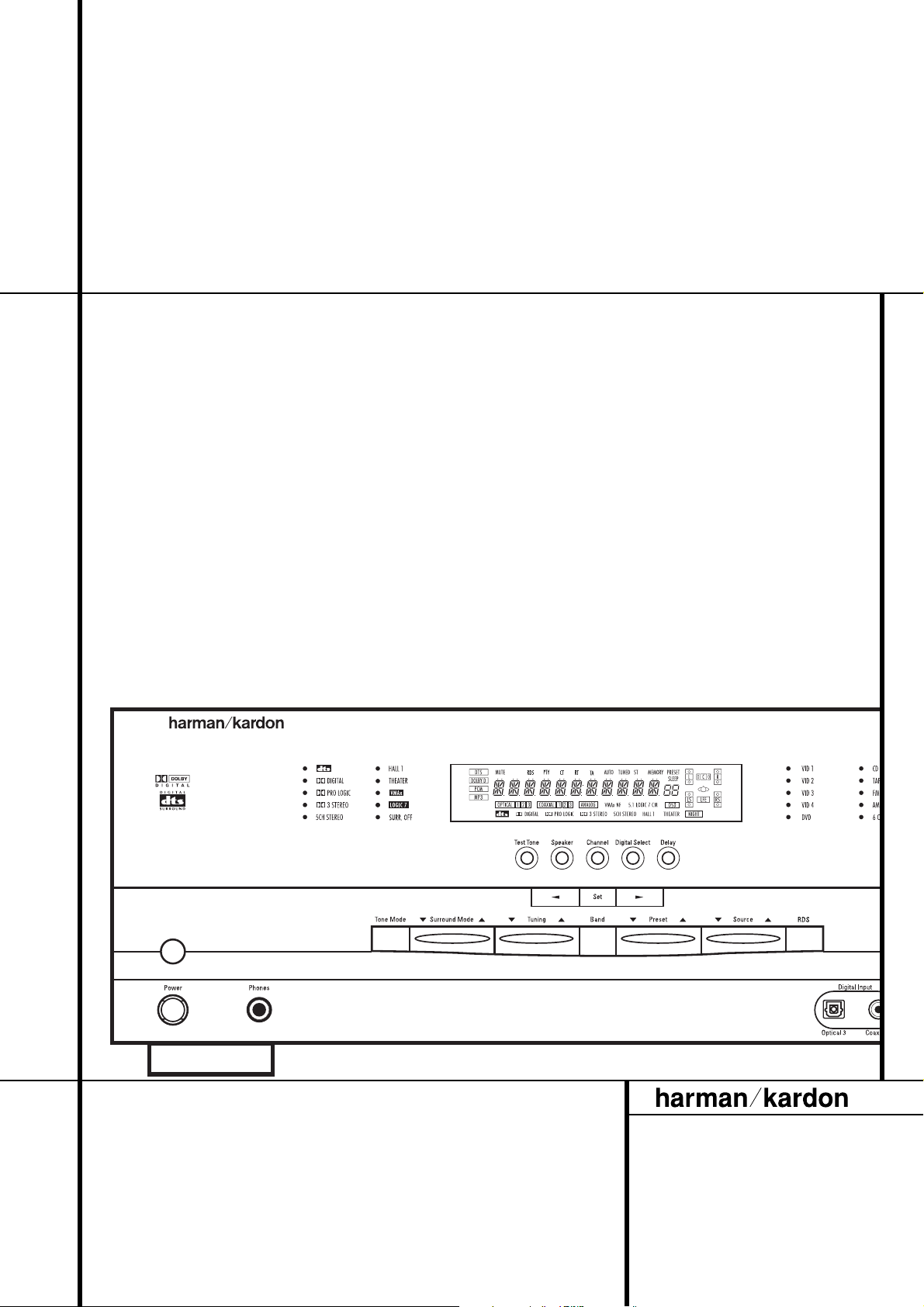
AMPLIFIER SECTION BIAS ADJUSTMENT
Measurement condition
. No input signal or volume position is minimum.
Standard value.
. Ideal current = 48mA ( ± 5%)
. Ideal DC Voltage = 21.12mV ( ± 5%)
CUP11517X (MAIN PCB)
CN63
CN62
VR62
VR64
CN64
VR61
CN61
VR63
DC VOLTMETER..............Connect to CN61, CN62, CN63, CN64, CN65
NO. Channel Adjust for
1 Front Left 21.12mV (±5%)
2 Front Right 21.12mV (±5%)
3 Center
4 Surround Left
5 Surround Right
21.12mV (±5%)
21.12mV (±5%)
21.12mV (±5%)
CN65
VR65
Adjustment
VR61
VR62
VR63
VR64
VR65
Page 5
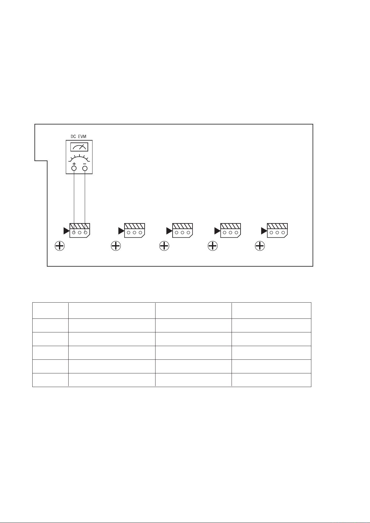
TRANSISTOR, REGULATOR IC BLOCK DIAGRAM
TO-92M
1. Emitter
2. Collector
3. Base
1. Emitter
2. Collector
3. Base
KTC2874B
KRA107M
2SA1360O
KTD600KG
KTD1302T
KTC3200GR
KTA1271Y
KTA1268GR
KTC3198Y
KSC2785Y
KRC107M
2SC3423O
1. Emitter
2. Collector
3. Base
TO-126
TO-92
123
123
123
1. Base
2. Collector
3. Emitter
KSA614Y
TO-220
123
1. INPUT
2. GND
3. OUTPUT
MC7815C MC7805C
TO-220
123
1. GND
2. INPUT
3. OUTPUT
MCNJM7905 MC7915C
TO-220
123
1. Base
2. Collector
3. Emitter
2SB1647 2SD2560
KTA1024Y KSC2316Y
1. Emitter
2. Collector
3. Base
TO-3P
TO-92L
123
123
Page 6
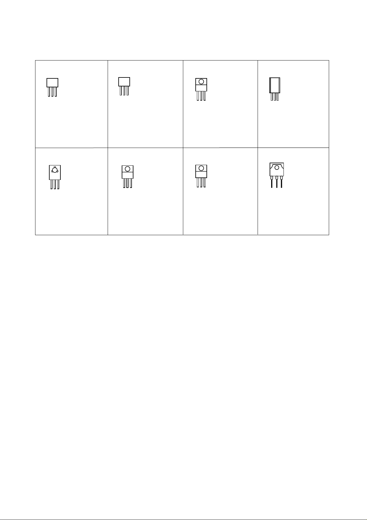
TC9482F (ELECTRONIC VOLUME/INPUT) : IC31
NC VSS VDD TEST
2
1
28 27
L-OUTA
L-INA
L-A-GNDA
L-OUTB
L-INB
L-A-GNDB
L-OUTC
L-INC
L-A-GNDC
CS1
GND
10
11
12
13
3
4
5
6
7
8
9
1dB
VR
latch
8dB
VR
latch
1dB
VR
latch
8dB
VR
latch
1dB
VR
latch
8dB
VR
latch
Shift register (32BIT)
Level shift circuit
3 to 7
decoder
4 to 13
decoder
Same as L-ch
Circuit
Strobe generate
circuit
3
4
5
6
7
8
9
10
11
12
13
L-OUTA
L-INA
L-A-GNDA
L-OUTB
L-INB
L-A-GNDB
L-OUTC
L-INC
L-A-GNDC
CS1
GND
CK
14
14
CK
Page 7
TC9215AF
TC9215AF (TONE CONTROL : IC80)
BLOCK DIAGRAM
GND 1
OFF 2
3S
10
S
4
11
S
5
12
S
6
20
S
7
21
V
8
ss
16 V
15
S
S
14
S
13
S
12
S
11
10
S
9
S
DD
40
41
42
34
32
31
30
Page 8
LEVEL SHIFTER
2
1
2
3
4
1
5
6
2
7
8
3
1
2
3
4
1
5
6
2
7
8
3
1
3
4
5
6
7
8
9
10
14 28
11
12
13
27
26
25
24
23
22
21
20
19
18
17
16
15
LATCH CIRCUIT
SHIFT REGISTER
LEVEL SHIFTER
LATCH CIRCUIT
L-S R-S
Vss GND VDD
L-S
L-S
L-S
L-COM
L-S
L-S
L-COM
L-S
L-S
L-COM
ST
R-S
R-S
R-S
R-COM
R-S
R-S
R-COM
R-S
R-S
R-COM
DATA
CK
LEVEL SHIFTER
2
1
2
3
1
4
5
6
2
7
8
3
1
2
3
1
4
5
6
2
7
8
3
1
3
4
5
6
7
8
9
10
14 28
11
12
13
27
26
25
24
23
22
21
20
19
18
17
16
15
LATCH CIRCUIT
SHIFT REGISTER
LEVEL SHIFTER
LATCH CIRCUIT
L-S R-S
Vss GND VDD
L-S
L-S
L-COM
L-S
L-S
L-S
L-COM
L-S
L-S
L-COM
ST
R-S
R-S
R-COM
R-S
R-S
R-S
R-COM
R-S
R-S
R-COM
DATA
CK
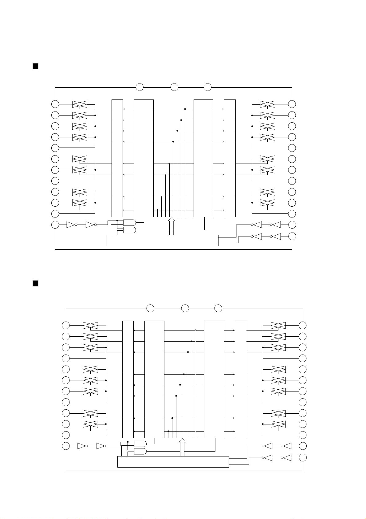
TC9164AF (FUNCTION/INPUT) : IC22
BLOCK DIAGRAM
TC9163AF (FUNCTION/INPUT) : IC20
BLOCK DIAGRAM
Page 9
LEVEL SHIFTER
2
1
2
1
3
4
2
5
6
3
7
4
1
2
1
3
4
2
5
6
3
7
4
1
3
4
5
6
7
8
9
10
14 28
11
12
13
27
26
25
24
23
22
21
20
19
18
17
16
15
LATCH CIRCUIT
SHIFT REGISTER
LEVEL SHIFTER
LATCH CIRCUIT
L-S R-S
Vss GND VDD
L-S
L-COM
L-S
L-S
L-COM
L-S
L-S
L-COM
L-S
L-COM
ST
R-S
R-COM
R-S
R-S
R-COM
R-S
R-S
R-COM
R-S
R-COM
DATA
CK
LEVEL SHIFTER
2
1
2
1
3
4
2
5
6
3
7
4
1
2
1
3
4
2
5
6
3
7
4
1
3
4
5
6
7
8
9
10
14 28
11
12
13
27
26
25
24
23
22
21
20
19
18
17
16
15
LATCH CIRCUIT
SHIFT REGISTER
LEVEL SHIFTER
LATCH CIRCUIT
L-S R-S
Vss GND VDD
L-S
L-COM
L-S
L-S
L-COM
L-S
L-S
L-COM
L-S
L-COM
ST
R-S
R-COM
R-S
R-S
R-COM
R-S
R-S
R-COM
R-S
R-COM
DATA
CK
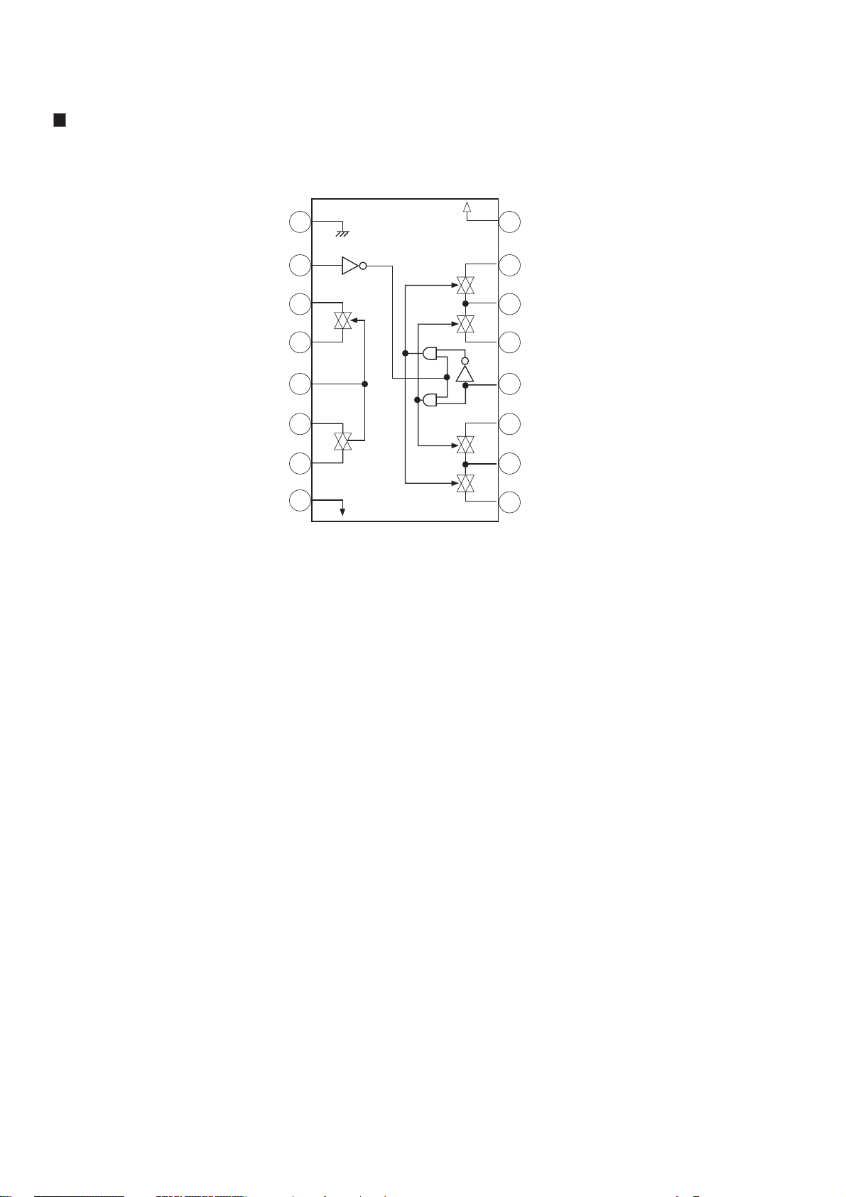
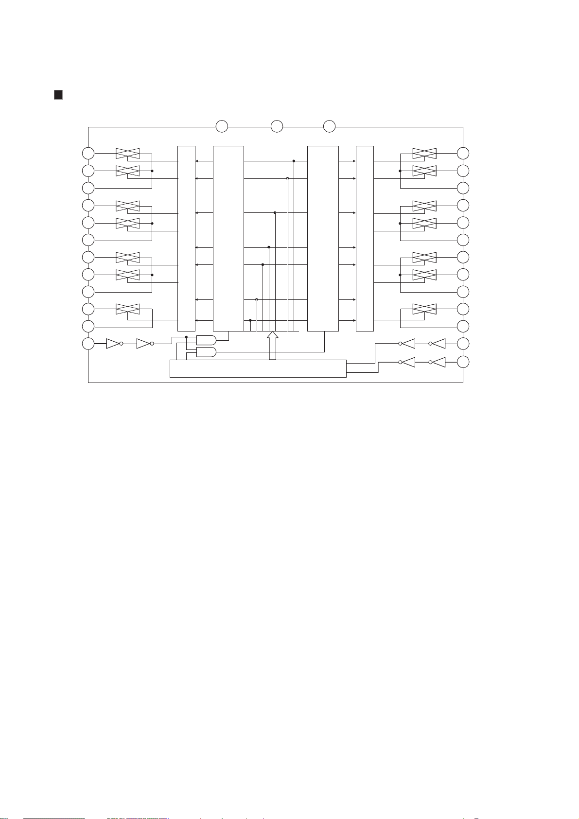
TC9162AF (FUNCTION/INPUT : IC30)
BLOCK DIAGRAM
TC9162AF (FUNCTION/INPUT : IC30)
BLOCK DIAGRAM
Page 10
No. 5606-3/13
Top view
PIN ASSIGNMENT (TOP VIEW)
Page 11
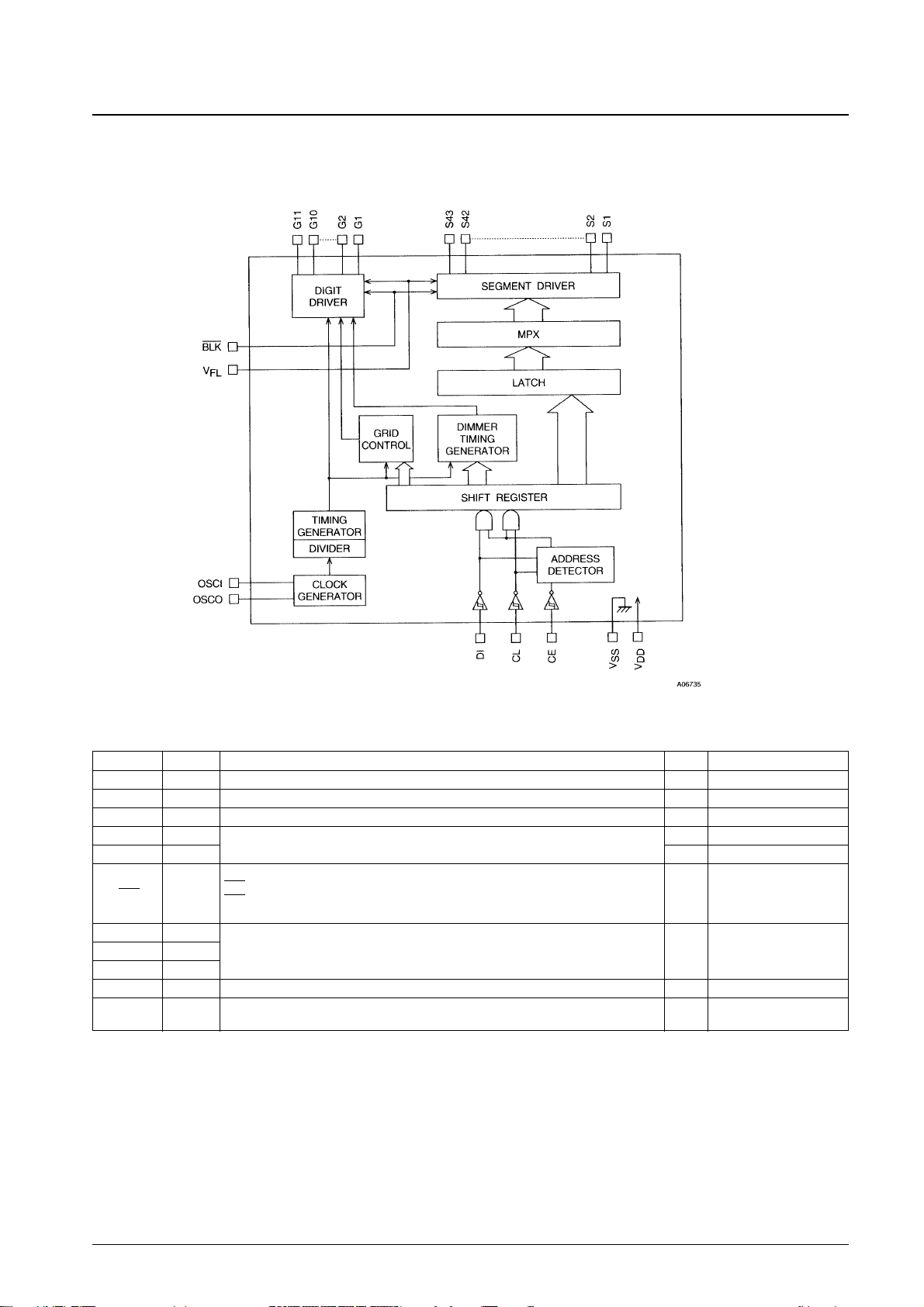
Pin Pin No. Function I/O Handling when unused
V
FL
1, 13 Driver block power supply connection. (Both pins must be connected.) — —
V
DD
60 Logic block power supply connection. Provide a voltage between 4.5 and 5.5 V. — —
V
SS
57 Power supply connection. Connect to the ground. — —
OSCI 59
Oscillator connection. An oscillator circuit is formed by connecting an external resistor
I GND
OSCO 58
and capacitor to these pins.
O OPEN
Display off control input.
BLK 61
BLK = Low (V
SS
) ... Display off. (S1 to S43 and G1 to G11 at VFLlevel.)
I GND
BLK = High (V
DD
) ... Display on.
Note that serial data can be transferred while the display is turned off.
CL 63
DI 64 I GND
CE 62
G1 to G11 2 to 12 Digit outputs. These pins are P-channel open drain outputs with pull-down resistors. O OPEN
S1 to S43 56 to 14
Segment outputs for displaying the display data transferred by serial data input. These pins
O OPEN
are P-channel open drain outputs with pull-down resistors.
Serial data transfer inputs. These pins must be connected to the system microcontroller.
CL: Synchronization clock
DI: Transfer data
CE: Chip enable
BLOCK DIAGRAM
VFD DRIVER IC PIN FUNCTION (LC75725E) : IC74
Page 12
PIN No. Pin Name I/O Function
1,12,23 +VD1 - Digital Power supply. Normally +2.5v
2,13,24 DGND - Digital Ground
3 AUD3 O SPDIF transmitter output/Digital audio output(N.C)
4 WR I Host write strobe pin(connected to GND with an external resistor)
5 RD I Host parallel output enable pin(pulled up with an external resistor)
6 CS_DA I SPI Serial data input pin
7 CS_CK I Serial control clock input pin
8 EMAD7 I/O
9 EMAD6 I/O
10 EMAD5 I/O
11 EMAD4 I/O Serial data IN/OUTPUT pins(pulled up with an external resistor)
14 EMAD3 I/O
15 EMAD2 I/O
16 EMAD1 I/O
17 EMAD0 I/O
18 CS_CE I Host parallel chip select pin
19 SCDIO(AK_DOUT) O Serial control port data ouput pin
20 INTREQ O Control port interrupt request output pin
21 EXTMEM I/O External Memory Chip Selector(pulled up with an external resistor)
22 SDATAN1(SDI) I PCM audio data input number 1 pin
25 SCLKN1(BICK) I PCM audio input bit clock pin
26 LRCLKN1(LRCK) I PCM audio input sample rate clock pin
27 CMPDAT(SDI) I PCM audio data input number 2 pin
28 CMPCLK(BICK) I PCM audio input bit clock pin
29 CREQ(LRCK) I PCM audio input sample rate clock pin
30 CLKIN(XIN) I Master clock input(used external clock)
31 CLKSEL(GND) I DSP clock mode select pin: connect the GND
32 FILT1 Connects to an external filter for the on-chip phase-locked loop
33 FILT1 Connects to an external filter for the on-chip phase-locked loop
34 +2.5V - Analog Power supply for clock generator . Normally +2.5V
35 AGND - Analog ground supply for clock generator PLL.
36 RESET(CS_RST) I Master reset input pin
37 DBDATA - Reserved pin and should be pulled up with an external resistor.
38 DBCLK - Reserved pin and should be pulled up with an external resistor.
39 AUD2(SDO2) O PCM multi-format digital-audio data ouput2 pin
40 AUD1(SDO1) O PCM multi-format digital-audio data ouput1 pin
41 AUD0(SDO0) O PCM multi-format digital-audio data ouput0 pin
42 LRCLK I Audio output sample rate clock pin
43 SCLK(BICK) I Audio ouput bit clock pin
44 MCLK I Audio master clock output pin
AUDIO DSP (CS493263 - CLG : IC79)
Page 13
PIN ASSIGNMENT.(CS493263)
(TOP VIEW)
BlOCK DIAGRAM(CS493263)
VD1
DGND1
AUDATA3, XMT958
WR,DS,EMWR,GPIO10
RD,R/W,EMOE,GPIO11
A1,SCDIN
A0,SCCLK
DATA7,EMAD7,GPIO7
DATA6,EMAD6,GPIO6
DATA5,EMAD5,GPIO5
DATA4,EMAD4,GPIO4
VD2
DGND2
DATA3,EMAD3,GPIO3
DATA2,EMAD2,GPIO2
DATA1,EMAD1,GPIO1
DATA0,EMAD0,GPIO0
CS
SCDIO,SCDOUT,PSEL,GPIO9
ABOOT,INTREQ
EXTMEM,GPIO8
SDATAN1
7
8
9
10
11
12
13
14
15
16
17
6 5 4 3 2 1 44 43 42 41 40
CS493XXX-CLG
44-pin PLCC
Top View
18 19 20 21 22 23 24 25 26 27 28
MCLK
SCLK
LRCLK
AUDATA0
AUDATA1
AUDATA2
DC
39
38
37
36
35
34
33
32
31
30
29
DD
RESET
AGND
VA
FILT1
FILT2
CLKSEL
CLKIN
CMPREQ,LRCLKN2
CMPCLK,SCLKN2
CMPDAT,SCLKN2,RCV958
LRCLKN1
SCLKN1,STCCLK2
DGND3
VD3
DATA7:0,
EMAD7:0,
GPIO7:0
Controller
RAM Input
PLL
CMPDAT
SDATAN2
CMPCLK
SCLKN2
CMPREQ
LRCLKN2
SCLKN1
STCCLK2
LRCLKN1
SDATAN1
CLKIN
CLKSEL
RESET
Compressed
Data Input
Interface
Digital
Audio
Input
Interface
Clock Manager
Framer
Shifter
Input
Buffer
Buffer
CS
RD,
R/W,
EMWR,
EMOE,
GPIO10
GPIO11
DSP Processing
RAM
Program
Memory
ROM
Program
Memory
WR,
DR,
SCDIO,
SCDOUT,
PSEL,
GPIO9
Parallel or Serial Host Interface
24-Bit
RAM
Data
Memory
ROM
Data
Memory
STC
A0,
SCCLK
Output
A1,
SCDIN
RAM
Buffer
A800T
INTERQ
EXTMEM.
GPIO8
Output
Formatter
DD
DC
MCLK
SCLK
LRCLK
AUDA
XMT95
FILTD FILTS VA AGND DGND(3:1) VD(3:1)
Page 14
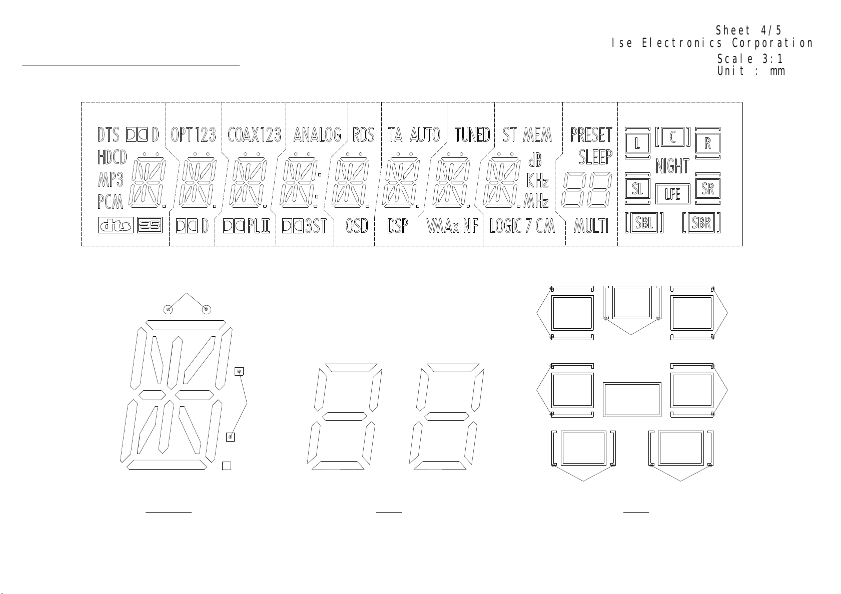
CM2054C
Ise Electronics Corporation
:Grid Assignment
G10 G9 G8 G7 G6 G5 G4 G3 G2 G1
S16
S18
S22
S15
S21
S15
Sheet 4/5
Scale 3:1
Unit : mm
S16
S10
S3
S7
S14
S1
S17
S3
S5
S1
S7
S4
S6
S2
S14
S12
S16
S13
S10
S15
S11
S4
S3 S9
S7 S13
S13
S11
S8
S5
S2
G3-G10 G2 G1
S12
S9
S6
S4
S19
S10
S1
S12S6
Page 15
Sheet 5/5
CM2054C
S1
S2
S3
S4
S5
S6
S7
S8
S9
S10
S11
S12
S13
S14
S15
S16
S17
S18
S19
S20
S21
S22
S23
S24
LFE
SBL
S10
S12
S13
SBR
S15
S16
S18
S19
S21
S22
NIGHT
:Anode & Grid Assignment
G1
S1
S3
S4
SL
S6
S7
S9
SR
R
C
L
G2 G3 G4 G5 G6 G7 G8 G9 G10
S1
S2
S3
S4
S5
S6
S7
S10
S11
S12
S13
S14
S15
S16
PRESET
SLEEP
MULTI
S1
S2
S3
S4
S5
S6
S7
S8
S9
S10
S11
S12
S13
S14
S15
S16
dB
ST
MEM
KHz
MHz
LOGIC 7
C
M
S10
S11
S12
S13
S14
S15
S16
TUNED
VMAx
S1
S2
S3
S4
S5
S6
S7
S8
S9
N
F
S1
S2
S3
S4
S5
S6
S7
S8
S9
S10
S11
S12
S13
S14
S15
S16
TA
AUTO
DSP
S1
S2
S3
S4
S5
S6
S7
S8
S9
S10
S11
S12
S13
S14
S15
S16
RDS
OSD
S1
S2
S3
S4
S5
S6
S7
S8
S9
S10
S11
S12
S13
S14
S15
S16
S17
ANALOG
3
ST
S1
S2
S3
S4
S5
S6
S7
S8
S9
S10
S11
S12
S13
S14
S15
S16
COAX
1
2
3
Ise Electronics Corporation
S1
S2
S3
S4
S5
S6
S7
S8
S9
S10
S11
S12
S13
S14
S15
S16
OPT
1
2
3
S1
S2
S3
S4
S5
S6
S7
S8
S9
S10
S11
S12
S13
S14
S15
S16
DTS
D
HDCD
MP3
PCM PL D
PIN ASSIGNMENT
Pin No.
Assignment F2 NP NL S24 S23 S22 S21 S20 S19 S18 S17 S16 S15 S14 S13 S12 S11 S10 S9 S8 S7 S6 S5 S4 S3 S2
Pin No.
Assignment NL NL NL NL G10 G9 G8 G7 G6 G5 G4 G3 G2 G1 NL NP F1
F1,F2:Filament G1-G10:Grid S1-S24:Anode NP:No Pin NL:No Lead
NL
(F2)
S1
12345678910111213141516171819
NL
(F1)
202122232425262728293031323334353637383940414243444546
Page 16

A/D CONVERTER IC (AK5380VT) : IC77
AINL
AINR
VCOM
AGNDVA
∆Σ
Modulator
∆Σ
Modulator
Voltage Reference
TST
DGNDVD
Decimation
Decimation
Filter
Filter
PDN
MCLK
Clock Divider
Serial I/O
Interface
TTL
DIF
LRCK
SCLK
SDTO
Page 17

PIN ASSIGNMENT (TOP VIEW)
A/D CONVERTER IC (AK5380VT) : IC77
AINL
NC
VCOM
AGND
VA
VD
DGND
1AINR
2
3
4
Top
16
15
14
13
TST
TTL
DIF
PDN
View
5
6
7
8
12
11
10
SCLK
MCLK
LRCK
9
SDTO
Page 18

PIN/FUNCTION
A/D CONVERTER IC PIN FUNCTION (AK5380VT) : IC77
No. Pin Name I/O Description
1 AINR I Rch Analog Input Pin
2 AINL I Lch Analog Input Pin
3 NC - NC Pin
No internal bonding.
4 VCOM O Common Voltage Output Pin
Normally connected to AGND with a 0.1µF ceramic capacitor in parallel with an
electrolytic capacitor less than 2.2µF.
5 AGND - Analog Ground Pin, 0V
6VA 7VD 8 DGND - Digital Ground Pin, 0V
9 SDTO O Serial Data Output Pin
10 LRCK I Left/Right Channel Select Pin
11 MCLK I Master Clock Input Pin
SCLK I Serial Data Input Pin
12
13 PDN I Power-Down Pin
14 DIF I Serial Interface Format Pin
15 TTL I Digital Input Level Select Pin
16 TST I Test Pin (Internal pull-down pin)
Analog Power Supply Pin, +4.5∼+5.5V
Digital Power Supply Pin, +2.7∼+5.5V(fs=48kHz), +4.5∼+5.5V(fs=96kHz)
Data bits are presented MSB first, in 2’s complement format.
This pin is “L” in the power-down mode.
The fs clock is input to this pin.
Output data is clocked out on the falling edge of SCLK.
When “L”, the circuit is in power-down mode.
The AK5380 should always be reset upon power-up.
“L”: MSB justified, “H”: I
“L”: CMOS level (VD=2.7∼5.5V), “H”: TTL level (VD=4.5∼5.5V)
This pin should be left open.
2
S
Note: All input pins except pull-down pins should not be left floating.
Page 19

O
n Block Diagram
DZFL1
LOUT1 +
LOUT1 DZFR1
ROUT1+
ROUT1-
DZFL2
LOUT2 +
LOUT2 DZFR2
ROUT2+
ROUT2-
DZFL3
LOUT3 +
LOUT3 DZFR3
ROUT3+
ROUT3-
SCF
SCF
SCF
SCF
DAC
DAC
DAC
DAC
SCF DAC
SCF DAC
DATT
DATT
DATT
DATT
DATT
DATT
Audio
I/F
AK4356
Control
Register
MCLK
LRCK
BICK
SDTI1
SDTI2
SDTI3
XTI
XTO
MCK
LRCK
BICK
CS
CCLK
CDTI
LRCK
BICK
SDOUT1
SDOUT2
SDOUT3
Controller
AC3
Page 20

ROUT
1+
C
C
ROUT
LOUT
LOUT
ROUT
ROUT
LOUT
LOUT
ROUT
ROUT
AVSS
19
D/A CONVERTER IC PIN ASSIGNMENT & BLOCK DIAGRAM
PIN ASSIGNMENT (TOP VIEW)
1-43
2+42
2-41
2+40
2-
3+38
3+36
3-35
3-
LOUT1LOUT1+
DZFL2 3
DZFR1 4
DZFL1
AD0 6
AD1 7
PDN 8
BICK
MCLK 10
DVDD 11
1
2
5
9
44
12
AK4356VQ
15
1132143
39
Top View
161718
37
20
CSN
21
0
34
22
0
33
32
31
30
29
28
27
26
25
24
23
AVDD
VREFH
DZFR2
DZFL3
DZFR3
DZFE
DIF2
DIF1
DIF0
CKS2
CKS1
Page 21

PIN/FUNCTION
D/A CONVERTER IC PIN FUNCTION (AK4356VQ) : IC78
No. Pin Name I/O Function
1 LOUT1- O DAC1 Lch Negative Analog Output Pin
2 LOUT1+ O DAC1 Lch Positive Analog Output Pin
3 DZFL2 O DAC2 Lc h Zero Input Detect Pin
4 DZFR1 O DAC1 Rch Zero Input Detect Pin
5 DZFL1 O DAC1 Lc h Zero Input Detect Pin
6 CAD0 I Chip Address 0 Pin
7 CAD1 I Chip Address 1 Pin
8 PDN I Power-Down & Reset Pin
When “L”, the AK4356 is powered-down and the control registers are reset to
default state. If the state of CAD0-1 changes, then the AK4356 must be reset by PDN.
9 BICK I Audio Serial Data Clock Pin
10 MCLK I Master Clock Input Pin
11 DVDD 12 DVSS - Digital Ground Pin
13 SDTI1 I DAC1 Audio Serial Data Input Pin
14 SDTI2 I DAC2 Audio Serial Data Input Pin
15 SDTI3 I DAC3 Audio Serial Data Input Pin
16 LRCK I Aud io Input Channel Clock Pin
17 SMUTE I Soft Mute Pin (Note)
18 CCLK I Control Data Clock Pin
19 CDTI I Control Data Input Pin
20 CSN I Chip Select Pin
Digital Power Supply Pin, +4.75~+5.25V
When this pin goes to “H”, soft mute cycle is initialized.
When returning to “L”, the output mute releases.
This pin should be held to “H” except for access.
Page 22

No. Pin Name I/O Function
21 DFS0 I Double Speed Sampling Mode 0 Pin (Note)
“L”: Normal Speed, “H”: Double Speed at DFS1 bit = “0”.
22 CKS0 I Input Clock Select 0 Pin (Note)
23 CKS1 I Input Clock Select 1 Pin (Note)
24 CKS2 I Input Clock Select 2 Pin (Note)
25 DIF0 I Audio Data Interface Format 0 Pin (Note)
26 DIF1 I Audio Data Interface Format 1 Pin (Note)
27 DIF2 I Audio Data Interface Format 2 Pin (Note)
28 DZFE I Zero Input Detect Enable Pin (Note)
29 DZFR3 O DAC3 Rch Zero Input Detect Pin
30 DZFL3 O DAC3 Lch Zero Input Detect Pin
31 DZFR2 O DAC2 Rch Zero Input Detect Pin
32 VREFH I Positive Voltage Reference Input Pin, AVDD
33 AVDD - Analog Power Supply Pin
34 AVSS -
Analog Ground Pin, +4.75~+5.25V
35 ROUT3- O DAC3 Rch Negative Analog Output Pin
36 ROUT3+ O DAC3 Rch Positive Analog Output Pin
37 LOUT3- O DAC3 Lch Negative Analog Output Pin
38 LOUT3+ O DAC3 Lch Positive Analog Output Pin
39 ROUT2- O DAC2 Rch Negative Analog Output Pin
40 ROUT2+ O DAC2 Rch Positive Analog Output Pin
41 LOUT2- O DAC2 Lch Negative Analog Output Pin
42 LOUT2+ O DAC2 Lch Positive Analog Output Pin
43 ROUT1- O DAC1 Rch Negative Analog Output Pin
44 ROUT1+ O DAC1 Rch Positive Analog Output Pin
Note:SMUTE, DFS0, CKS0, CKS1, CKS2, DIF0, DIF1, DIF2, DZFE pins are ORed with serial control register.
Page 23

Oscillator
P/S=”L”
Oscillator
P/S=”H”
BLOCK DIAGRAM
RX0
RX1
RX2
RX3
RX4
RX5
RX6
RX7
TX0
TX1
DVDD
DVSS
TVDD
8 to 3
Input
Selector
DIT
VIN
RAVDDAVSS
Clock
Recovery
DAIF
Decoder
B,C,U,VOUT
AC-3/MPEG
Detect
DEM
INT0
X'tal
Error &
STATUS
Detect
INT1
XTOXTI
Q-subcode
buffer
Clock
Generator
Audio
I/F
µP I/F
MCKO1
MCKO2
LRCK
BICK
SDTO
DAUX
PDN
CSN
CCLK
CDTO
CDTI
IIC
RX0
RX1
RX2
RX3
IPS0
DIF0
DIF1
DIF2
TX0
TX1
DVDD
DVSS
TVDD
4 to 2
Input
Selector
DIT
Serial Control Mode
RAVDDAVSS
Clock
Recovery
DAIF
Decoder
AC-3/MPEG
Detect
DEM
X'tal
Error &
STATUS
Detect
XTOXTI
Clock
Generator
Audio
I/F
MCKO1
MCKO2
LRCK
BICK
SDTO
DAUX
PDN
OCKS0
OCKS1
CM0
CM1
VIN
B,C,U,VOUT
INT0
Parallel Control Mode
INT1
IPS1
Page 24

D
C
T
T
T
D
DVSS
T
LRCK
DIR IC PIN ASSIGNMENT & BLOCK DIAGRAM
PIN ASSIGNMENT (TOP VIEW)
22
INT1
37
38
36
35
34
33
32
31
30
29
28
27
26
24
MCKO1 23
RX3
AVSS
TEST1
RX1
RX2
46
IPS0/RX4
AVSS
DIF0/RX5 3
TEST2 4
DIF1/RX6
AVSS 6
DIF2/RX7 7
IPS1/IIC 8
P/SN
XTL0 10
XTL1
VIN 12 25 SDTO
48
1
2
5
9
11
13
TVD
47
14
N
TX015TX1
45
AK4114VQ
16
AVSS
44
43
Top View
17
18
BOU
COU
RX0
42
19
UOU
VCOM40R39AVDD
AVSS
41
20
21
VOU
DVD
INT0
OCKS0/CSN/CAD0
OCKS1/CCLK/SCL
CM1/CDTI/SDA
CM0/CDTO/CAD1
PDN
XTI
XTO
DAUX
MCKO2
BICK
Page 25

DIR IC PIN FUNCTION (AK4114VQ) : IC75
PIN/FUNCTION
No. Pin Name I/O Function
IPS0 I Input Channel Select 0 Pin in Parallel Mode
1
RX4 I Receiver Channel 4 Pin in Serial Mode (Internal biased pin)
2 NC(AVSS) I
DIF0 I Audio Data Interface Format 0 Pin in Parallel Mode
3
RX5 I Receiver Channel 5 Pin in Serial Mode (Internal biased pin)
4 TEST2 I
DIF1 I Audio Data Interface Format 1 Pin in Parallel Mode
5
RX6 I Receiver Channel 6 Pin in Serial Mode (Internal biased pin)
6 NC(AVSS) I
DIF2 I Audio Data Interface Format 2 Pin in Parallel Mode
7
RX7 I Receiver Channel 7 Pin in Serial Mode (Internal biased pin)
IPS1 I Input Channel Select 1 Pin in Parallel Mode
8
IIC I
9 P/SN I
10 XTL0 I X’tal Frequency Select 0 Pin
11 XTL1 I X’tal Frequency Select 1 Pin
12 VIN I V-bit Input Pin for Transmitter Output
13 TVDD I Input Buffer Power Supply Pin, 3.3V or 5V
14 NC I
15 TX0 O Transmit Channel (Through Data) Output 0 Pin
16 TX1 O
17 BOUT O
18 COUT O C-bit Output Pin for Receiver Input
19 UOUT O U-bit Output Pin for Receiver Input
20 VOUT O V-bit Output Pin for Receiver Input
21 DVDD I Digital Power Supply Pin, 3.3V
22 DVSS I Digital Ground Pin
23 MCKO1 O Master Clock Output 1 Pin
24 LRCK I/O Channel Clock Pin
25 SDTO O Audio Serial Data Output Pin
26 BICK I/O Audio Serial Data Clock Pin
27 MCKO2 O Master Clock Output 2 Pin
28 DAUX I Auxiliary Audio Data Input Pin
29 XTO O X'tal Output Pin
30 XTI I X'tal Input Pin
No Connect
No internal bonding. This pin should be connected to AVSS.
TEST 2 pin
This pin should be connect to AVSS.
No Connect
No internal bonding. This pin should be connected to AVSS.
IIC Select Pin in Serial Mode.
“L”: 4-wire Serial, “H”: IIC
Parallel/Serial Select Pin
“L”: Serial Mode, “H”: Parallel Mode
No Connect
No internal bonding. This pin should be open or connected to DVSS.
When TX bit = “0”, Transmit Channel (Through Data) Output 1 Pin.
When TX bit = “1”, Transmit Channel (DAUX Data) Output Pin (Default).
Block-Start Output Pin for Receiver Input
“H” during first 40 flames.
Page 26

PIN/FUNCTION (Continued)
No. Pin Name I/O Function
31 PDN I
CM0 I Master Clock Operation Mode 0 Pin in Parallel Mode
CDTO O Control Data Output Pin in Serial Mode, IIC= “L”.32
CAD1 I Chip Address 1 Pin in Serial Mode, IIC= “H”.
CM1 I Master Clock Operation Mode 1 Pin in Parallel Mode
CDTI I Control Data Input Pin in Serial Mode, IIC= “L”.33
SDA I/O Control Data Pin in Serial Mode, IIC= “H”.
OCKS1 I Output Clock Select 1 Pin in Parallel Mode
CCLK I Control Data Clock Pin in Serial Mode, IIC= “L”34
SCL I Control Data Clock Pin in Serial Mode, IIC= “H”
OCKS0 I Output Clock Select 0 Pin in Parallel Mode
CSN I Chip Select Pin in Serial Mode, IIC=”L”.35
CAD0 I Chip Address 0 Pin in Serial Mode, IIC= “H”.
36 INT0 O Interrupt 0 Pin
37 INT1 O Interrupt 1 Pin
38 AVDD I Analog Power Supply Pin, 3.3V
39 R -
40 VCOM -
41 AVSS I Analog Ground Pin
42 RX0 I
43 NC(AVSS) I
44 RX1 I Receiver Channel 1 Pin (Internal biased pin)
45 TEST1 I
46 RX2 I Receiver Channel 2 Pin (Internal biased pin)
47 NC(AVSS) I
48 RX3 I Receiver Channel 3 Pin (Internal biased pin)
Note 1. All input pins except internal biased pins should not be left floating.
Power-Down Mode Pin
When “L”, the AK4114 is powered-down and reset.
External Resistor Pin
18kΩ +/-1% resistor should be connected to AVSS externally.
Common Voltage Output Pin
0.47µF capacitor should be connected to AVSS externally.
Receiver Channel 0 Pin (Internal biased pin)
This channel is default in serial mode.
No Connect
No internal bonding. This pin should be connected to AVSS.
TEST 1 pin.
This pin should be connected to AVSS.
No Connect
No internal bonding. This pin should be connected to AVSS.
Page 27

PIN ASSIGNMENT (74HCU04AFN : IC71,72 )
1
1A
2
1Y
3
2A
4
2Y
5
3A
6
3Y
14
13
12
11
10
9
Vcc
6A
6Y
5A
5Y
4A
LOGIC SYMBOL
GND
1A
2A
3A
4A
5A
6A
7
(1)
(3)
(5)
(9)
(11)
(13)
8
(2)
(4)
(6)
(8)
(10)
(12)
4Y
1Y
2Y
3Y
4Y
5Y
6Y
TRUTH TABLE
A
L
H
Y
H
L
Page 28

Page 29

Page 30

DISASSEMBLY
1) REMOVAL OF TOP COVER
2) REMOVAL OF FRONT PANEL
3) PRINCIPAL PARTS LOACTION
TRANS FORMER
FRONT PCB
TUNER
MODULE
INPUT PCB
MAIN PCB
Page 31

Page 32

Page 33

AVR2550 Front board sch
Page 34

AVR2550 Main board sch
Page 35

AVR2550 Input board sch
Page 36

AVR2550 Video board sch
Page 37

AVR 2550 EXPLODE VIEW
Page 38

■ ELECTRICAL PARTS LIST
REF NO. PART NO. DESCRIPTION REMARKS
CUP11516X PCB , FRONT
▶CAPACITOR
C701,702 HCBS1H390JT CAP , CERAMIC 39PF 50V J
C703 HCBS1H821KBT CAP , CERAMIC 820PF 50V K
C704,735,773,774
777 778 864
C705,711 HCBS1H102KBT CAP , CERAMIC 1000PF 50V B
C706 HCBS1H561KBT CAP , CERAMIC 560PF 50V K
C707,783,784 HCBS1H101KBT CAP , CERAMIC 100PF 50V K
C708,713,730,732
736 770 771 805
806,859~862
C709,810,811 HCEA1CH101T CAP , ELECT 100UF 16V
C710 HCEA1HH2R2T CAP , ELECT 2.2UF 50V
C712 HCEA1HH1R0T CAP , ELECT 1UF 50V
C714,775,776 HCBS1H151KBT CAP , CERAMIC 150PF 50V K
C813,814 HCEA1HH4R7T CAP , ELECT 4.7UF 50V
C716,872,873 HCEA1CH331T CAP , ELECT 330UF 16V
C719~721 HCBS1H181KBT CAP , CERAMIC 180PF 50V K
C722 HCBS1H220JT CAP , CERAMIC 22PF 50V J
C723 CCFT1H104ZF CAP , SEMI 0.1UF 50V ZF
C725,729,865 CCKT1H473ZF CAP , CERAMIC 0.047UF 50V ZF
C726,863,886 HCEA0JH102T CAP , ELECT 1000UF 6.3V
C731 HCEA1HH100T CAP , ELECT 10UF 50V
C733 HCEA1EH470T CAP , ELECT 47UF 25V
C737,738 HCBS1H180JT CAP , CERAMIC 18PF 50V J
C779,780,791,792
868 869
C781,782,787~790
866 867
C785,786 HCBS1H470JT CAP , CERAMIC 47PF 50V J
C793,794,799,800 KCFE1J183JBT CAP , FILM 0.018UF 63V J
C795,796 KCFE1J823JBT CAP , FILM 0.082UF 63V J
C797,798 KCFE1J332JBT CAP , FILM 0.0033UF 63V J
C850,851 HCBS1H471KBT CAP , CERAMIC 470PF 50V K
C852,874,882,883 HCBS1H104ZFT CAP , CERAMIC 0.1UF 50V Z
C870,871 HCBS1H681KBT CAP , CERAMIC 680PF 50V K
C875~878 HCBS1H103ZFT CAP , CERAMIC 0.01UF 50V Z
C880 HCEA1AH221T CAP , ELECT 220UF 10V
C734,885 BCES0HD104 CAP , GOLD JP EECS0HD104V
C853 KCKDKS472ME CAP , CERAMIC(X1/Y2/SC) 0.0047UF/2.5KV
▶DIODE
D701~703,705~716
718~720,729~754
756~758
HCEA1VH100T CAP , ELECT 10UF 35V
HCBS1H223ZFT CAP , CERAMIC 0.022UF 50V Z
HCEA1CKS470T CAP, ELECT 47UF 16V
HCEA1CKS100T CAP , ELECT 10UF 16V
CVD30BSGATAAT L.E.D , GREEN (TAPPING)
Page 39

D761,777,779 HVD1SS133MT DIODE 1SS133T-77
D776,778 KVD1N4003ST DIODE 1N4003
D723 CVD50BOGDWGA L.E.D , 2 COLOR
▶COIL
L702 HLQ02C100KT COIL , AXAIL 10UH K
▶TRANSISTOR
Q701~703,705~716
718~720,724~729
HVTKRC107MT T.R
KRC107M
Q734~737 HVTKTC2874BT T.R , MUTE KTC2874B
▶RESISTOR
R701~703,705~716
718~720,826,827
CRD20TJ121T RES , CARBON 120 OHM 1/5W J
R704,757,763 CRD20TJ332T RES , CARBON 3.3K OHM 1/5W J
R723,732,847,848
853 854
R724,727,753,759
766 865 903 904
CRD20TJ222T RES , CARBON 2.2K OHM 1/5W J
CRD20TJ102T RES , CARBON 1K OHM 1/5W J
R725,726,734,735
744~747,771~773
CRD20TJ103T RES , CARBON 10K OHM 1/5W J
881~891
R728,810,811,822,
837,838,895~898
CRD20TJ101T RES , CARBON 100 OHM 1/5W J
R730,833,834 CRD20TJ112T RES , CABON 1.1K OHM 1/5W J
R731,749~751
849 850 913
R733,736,756,762
769 864 866
CRD20TJ223T RES , CARBON 22K OHM 1/5W J
CRD20TJ272T RES , CARBON 2.7K OHM 1/5W J
R737,892,893 CRD20TJ100T RES , CARBON 10 OHM 1/5W J
R754,760,767
901 902
CRD20TJ152T RES , CARBON 1.5K OHM 1/5W J
R755,761,768 CRD20TJ182T RES , CARBON 1.8K OHM 1/5W J
R758,764,823
831 832 907 908
CRD20TJ562T RES , CARBON 5.6K OHM 1/5W J
918 919
R765 CRD20TJ752T RES , CARBON 7.5K OHM 1/5W J
R775~800,802~804 CRD20TJ151T RES , CARBON 150 OHM 1/5W J
R813,814,839,840
845 846 899 900
CRD20TJ104T RES , CARBON 100K OHM 1/5W J
905 906
R824 CRD20TJ471T RES , CARBON 470 OHM 1/5W J
R825 CRD20TJ181T RES , CARBON 180 OHM 1/5W J
R829,830,835,836 CRD20TJ184T RES , CARBON 180K OHM 1/5W J
R841,842,914~916 CRD20TJ473T RES , CARBON 47K OHM 1/5W J
R843,844 CRD20TJ105T RES , CARBON 1M OHM 1/5W J
R851,852 CRD20TJ392T RES , CARBON 3.9K OHM 1/5W J
R855,856 CRD20TJ681T RES , CARBON 680 OHM 1/5W J
R857,858,909~912 CRD20TJ221T RES , CARBON 220 OHM 1/5W J
Page 40

R894 CRD20TJ1R0T RES , CARBON 1 OHM 1/5W J
G
1
)
R917 CRD20TJ123T RES , CARBON 12K OHM 1/5W J
▶SWITCH
S701~721 CST1A012ZT SW , TACT SKHV10910G
SW01 HSH1A008ZV SW , PUSH (MOMS)
▶WIRE ASS'Y
BN16 CWZAVR2550BN16 WIRE ASS'Y (SHIELD)
BN80 CWB2B908320EW WIRE ASS'Y
BN81 CWB2B906250BM WIRE ASS'Y
BN83 CWB1C902250BM WIRE ASS'Y
BN84 CWB2B905100EN WIRE ASS'Y
BN85,90 CWB2B902090EN WIRE ASS'Y
BN87 CWZAVR2550BN87 WIRE ASS'Y (SHIELD)
BN88 CWB2B904070EN WIRE ASS'Y
BN89 CWB2B905080EN WIRE ASS'Y
JW82 CWZAVR2550JW82 WIRE , ASS'Y
▶CONNECTOR
BN94 KJP10GB99ZM WAFER MOLEX35237-1010
BN95 KJP08GB99ZM CONNECTOR , HOUSING MOLEX35237-0810
CN11 KJP09GA98ZM WAFER MOLEX35336-0910
CN12 KJP14GA98ZM WAFER MOLEX35336-1410
CN16 KJP08GB46ZM WAFER MOLEX53015-0810
CN72 KJP32GA117ZG WAFER , CARD CABLE GF102-32S-TS
CN82 KJP06HA37ZM WAFER MOLEX42140-2206
CN84,89 KJP05GA19ZM WAFER MOLEX53014-0510
CN85,90 KJP02GA19ZM WAFER MOLEX53014-0210
CN86 KJP02GA89ZM WAFER MOLEX35328-02
CN87 KJP06GA19ZM WAFER MOLEX53014-0610
CN88 KJP04GA19ZM WAFER MOLEX53014-0410
▶F.I.P
FIP1 HFLCM2054C F.I.P
▶I.C
IC85 HVIRE5VT15CATZ IC , RESET RE5VT15CATZ
IC87 HVIRE5VL28CATZ IC , RESET RE5VL28CATZ
IC71 BVISAA6579TV1 I.C , RDS FILTER TW SAA6579T/V1
IC72 BVIMB90F476APF
IC , FLASH U-COM FUJITSU
IC73 HRVRPM6938H4 SENSOR , REMOTE RPM6938-H4
IC74 HVILC75725E IC , VFL DRIVER LC75725E
IC80 HVITC9215AF I.C TC9215AF
IC81,82,88 HVINJM2068MTE1 I.C , OP AMP NJM2068M-TE1
IC83,84 HVI74ACT04SC I.C , HEX INVERTER 74ACT04SC
IC86 HVINJM4556AMTE
I.C , OP AMP NJM4556AM-TE1
▶JACK
JK83 HJJ2E020Z JACK , HEADPHONE HTJ-064-05NG
▶VARIABLE RESISTOR
VR71 CVV2X05M104Z RES , VARIABLE(BALANCE
RK14128030214Y
Page 41

VR72,73 CVV2X07C104Z RES , VARIABLE(TONE) RK14128030214C
D
▶ENCODER
VR74 HSR2A023Z VR , ENCODER
▶CRYSTAL
X701 HOX04194E120C CRYSTAL
X702 HOX04332E200C CRYSTAL
CUP11517X PCB , MAIN
▶CAPACITOR
C501~505 HCEA1VH100T CAP , ELECT 10UF 35V
C506~510 CCKT1H331KB CAP , CERAMIC 330PF 50V KB
C561~565,907 HCEA1CH101T CAP , ELECT 100UF 16V
C566~570 HCEA1EH470T CAP , ELECT 47UF 25V
C571~575 CCKT1H681KB CAP , CERAMIC 680PF 50V KB
C601~605 CCCT1H120JC CAP , CERAMIC 12PF 50V JC
C606~610 CCCT1H330JC CAP , CERAMIC 33PF 50V JC
C641~645,681~685 HCEA1HH100T CAP , ELECT 10UF 50V
C826 HCQI1H182JZT CAP , MYLAR 1800PF 50V J
C901,998 CCFT1H104ZF CAP , SEMI 0.1UF 50V ZF
C905,908,923,925
963 999
CCKT1H223ZF CAP , CERAMIC 0.022UF 50V ZF
C911 HCEA1CH471T CAP , ELECT 470UF 16V
C912 HCEA1CH221T CAP , ELECT 220UF 16V
C922,924,962 HCEA1EH101T CAP , ELECT 100UF 25V
C938,991 HCEA1HH1R0T CAP , ELECT 1UF 50V
C939 HCEA1HH4R7T CAP , ELECT 4.7UF 50V
C940 HCEA1AH471T CAP , ELECT 470UF 10V
C971~975 HCQI1H562JZT CAP , MYLAR 5600PF 50V J
C976~979,993~997 HCQI1H473JZT CAP , MYLAR 0.047UF 50V J
C631~640 HCEA1JH221E CAP , ELECT 220UF 63V
C903 BCQE2E104KDE CAP , LINE ACROSS 0.1UF 250V KD
C904 KCKDKS472ME CAP , CERAMIC(X1/Y2/SC) 0.0047UF/2.5KV
C906 HCEA1EH102E CAP , ELECT 1000UF 25V
C915,916 HCET63VFHS123N
CAP , ELECT 2000UF 63V
C917 HCEA1EH332E CAP , ELECT 3300UF 25V
C918 HCEA1EH222E CAP , ELECT 2200UF 25V
C961 HCEA1CH472E CAP , ELECT 6800UF 16V
▶DIODE
D501~505,581~585
902 911 912 914 915
HVD1SS133MT DIODE 1SS133T-77
916,953~955
D901,903~906
961~963
KVD1N4003ST DIODE 1N4003
D956 KVD1N4003SRT DIODE TW 1N4003
▶TRANSISTOR
Q501~505,601~605 HVTKTA1268GRT T.R KTA1268GR
Q511~520,556~565 HVTKTC3200GRT T.R KTC3200GR
Q541~545 HVTKTC3198YT T.R KTC3198Y
Page 42

Q681~685,901
942 943
KVTKSC2785YT T.R KSC2785Y
Q806,969~973 HVTKTC2874BT T.R , MUTE KTC2874B
Q938,939,952,992 HVTKRA107MT T.R KRA107M
Q951,960,991 HVTKRC107MT T.R KRC107M
Q961 HVTKTA1024YT T.R KTA1024Y
Q611~615 HVTKTD600KGR T.R , BIAS KTD600KGR
Q621~625 HVT2SA1360O T.R 2SA1360O
Q626~630 HVT2SC3423O T.R 2SC3423O
Q652~655,661 BVT2SB1560 T.R , POWER 2SB1560
Q657~660,670 BVT2SD2390 T.R , P0WER 2SD2390
▶RESISTOR
R501~505 CRD20TJ433T RES , CARBON 43K OHM 1/5W J
R506~510 CRD20TJ333T RES , CARBON 33K OHM 1/5W J
R511~520,940 CRD20TJ152T RES , CARBON 1.5K OHM 1/5W J
R521~525,806
974~978
CRD20TJ471T RES , CARBON 470 OHM 1/5W J
R527~530,621~626 CRD20TJ750T RES , CARBON 75 OHM 1/5W J
R531~540 CRD20TJ221T RES , CARBON 220 OHM 1/5W J
R541~545 CRD20TJ271T RES , CARBON 270 OHM 1/5W J
R556~560,962 CRD20TJ273T RES , CARBON 27K OHM 1/5W J
R561~565,678~680 CRD20TJ182T RES , CARBON 1.8K OHM 1/5W J
R566~575,581~600
987
CRD20TJ561T RES , CARBON 560 OHM 1/5W J
R576~580 CRD20TJ100T RES , CARBON 10 OHM 1/5W J
R601~610,941~943
945
CRD20TJ223T RES , CARBON 22K OHM 1/5W J
R611~615,961 CRD20TJ331T RES , CARBON 330 OHM 1/5W J
R616~620 CRD20TJ122T RES , CARBON 1.2K OHM 1/5W J
R631~640 KRD25FJ180T RES , CARBON 18 OHM 1/4W J
R646~655 KRD25FJ3R3T RES , CARBON 3.3 OHM 1/4W J
R656~660 KRF5EKR22HX2 RES , CEMENT(*2) 0.22/5W *2
R905,993~997 KRG1ANJ100H RES , METAL OXIDE FILM 10 OHM 1W J
R666~670,696~700 CRD25TJ470T RES , CARBON 47 OHM 1/4W J
R671~675 CRD20TJ911T RES , CARBON 910 OHM 1/5W J
R676,677 CRD25TJ182T RES , CARBON 1.8K OHM 1/4W J
R681~685,960.992 CRD20TJ562T RES , CARBON 5.6K OHM 1/5W J
R686~690,930,932
966 998
CRD20TJ103T RES , CARBON 10K OHM 1/5W J
R816,939,969~973 CRD20TJ472T RES , CARBON 4.7K OHM 1/5W J
R826,979~983 CRD20TJ473T RES , CARBON 47K OHM 1/5W J
R910,963 CRD20TJ105T RES , CARBON 1M OHM 1/5W J
R911 CRD20TJ820T RES , CARBON 82 OHM 1/5W J
R913,914 CRD20TJ153T RES , CARBON 15K OHM 1/5W J
R917~920 CRD25TJ393T RES , CARBON 39K OHM 1/4W J
R944 CRD25TJ223T RES , CARBON 22K OHM 1/4W J
R986 CRD20TJ102T RES , CARBON 1K OHM 1/5W J
R988 CRD20TJ303T RES , CARBON 30K OHM 1/5W J
Page 43

R991 CRD20TJ822T RES , CARBON 8.2K OHM 1/5W J
M
S
▶SEMI RESISTOR
VR61~65 HVN1RA221B01T RES , SEMI FIXED(220 OH
RH0615C100221
▶WIRE ASS'Y
BN20 CWB3FB03280UP WIRE ASS'Y
BN90 CWB4D232450PU WIRE ASS'Y
JW91 CWE8212230VV WIRE ASS'Y
JW92 CWEE212120VV WIRE ASS'Y
▶CONNECTOR
CN61~65 KJP03GA01ZM WAFER MOLEX 5267-03A
CN80 KJP08GA19ZM WAFER MOLEX53014-0810
CN91 KJP02KA060ZY WAFER 7.92MM(YUNHO)
CN92 KJP02GA89ZM WAFER MOLEX35328-02
CN94 KJP10GA98ZM WAFER MOLEX35336-1010
CN95 KJP08GA98ZM WAFER MOLEX35336-0810
CN96 KJP07GA01ZM WAFER MOLEX 5267-07A
▶I.C
IC91 HVIMC7815C I.C, REGULATOR KA7815-ABTU
IC92 HVIMC7915C I.C, REGULATOR KA7915-ABTU
IC93,94 HVIMC7805C I.C, REGULATOR KA7805-ABTU
▶JACK
JK91 CJJ5N009Z TERMINAL , SPEAKER
JK92 CJJ5Q011Z TERMINAL , SPEAKER
JK93 CJJ4M040Z JACK , BOARD (SW)
▶COIL
L501~505 CLEY0R5KAK COIL , SPEAKER 0.5UH K
▶OUTLET
OL91 KJJ7A025Z OUTLET , EUR(2P) A3-04-D007-2P
▶RELAY
RY94 HSL1A008ZE RELAY SDT-S-112DMR
▶POSISTOR
TH91 KRTP42T7D330B THERMAL SENSOR , POSI
P42T7D330BW20
▶SUB TRANS
T902 CLT5J033ZE TRANS , SUB
CUP11518W PCB , INPUT
▶CAPACITOR
C201~206,211~218
321,322,325,326
CCKT1H221KB CAP , CERAMIC 220PF 50V KB
C231~236,349,350,799
382~386,390,421,426
440,447,452,454,456
HCEA1CH101T CAP , ELECT 100UF 16V
708,709,712,728,731
733,752,754,780,783
C237,240,359,361,362
387,703,705
CCKT1H181KB CAP , CERAMIC 180PF 50V KB
C238,239,335,360 CCKT1H471KB CAP , CERAMIC 470PF 50V KB
C261~272 HCEA1EH220T CAP , ELECT 22UF 50V
Page 44

C273~284 HCQI1H332JZT CAP , MYLAR 3300PF 50V J
C285,286,288~292
294~296,333
CCKT1H561KB CAP , CERAMIC 560PF 50V KB
C287,293,371 HCQI1H182JZT CAP , MYLAR 1800PF 50V J
C297~302,323,324,327
328,334,347,348,358
420,430,439,446,449
0.022UF 50V ZHCBS1H223ZFT CAP , CERAMIC
460,730,766
C303~308 HCEA1HH220T CAP , ELECT 22UF 50V
C336,357,461,735,921 CCKT1H223ZF CAP , CERAMIC 0.022UF 50V ZF
C339,340,772 HCBS1H103ZFT CAP , CERAMIC 0.01UF 50V Z
C343~346,351~356
769,363~368,375~380
416,419,425,438
HCEA1VH100T
CAP , ELECT 10UF 35V
441,443,445,448
453,455,762
C372~374 CCKT1H151KB CAP , CERAMIC 150PF 50V KB
C388,389 HCEA1CH471T CAP , ELECT 470UF 16V
C395 HCEA1HH1R0T CAP , ELECT 1UF 50V
C418,431,442,444
458,726,776
CCKT1H101KB
CAP , CERAMIC
100PF 50V KB
C457,721,737 HCBS1H101KBT CAP , CERAMIC 100PF 50V K
C701,702,781,784 HCEA1AH471T CAP , ELECT 470UF 10V
C704,706,707,734,755
756,761,773,774
CCFT1H104ZF CAP , SEMI
0.1UF 50V ZF
901,902
C710,778,785 CCKT1H473ZF CAP , CERAMIC 0.047UF 50V ZF
C711,713,714,717 CCCT1H270JC CAP , CERAMIC 22PF 50V JC
C715,782 HCBS1H473ZFT CAP , CERAMIC 0.047UF 50V Z
C719,720,727,729,732
736,740,743,744,746
747,751,763,768,779
HCBS1H104ZFT CAP , CERAMIC
0.1UF 50V Z
786,787
C722,723 CCCT1H100DC CAP , CERAMIC 10PF 50V DC
C724 HCBS1H330JT CAP , CERAMIC 33PF 50V J
C725 CCCT1H330JC CAP , CERAMIC 33PF 50V JC
C741,742 HCEA1EH470T CAP , ELECT 47UF 25V
C745,770 HCEA1HH2R2T CAP , ELECT 2.2UF 50V
C764,765 CCCT1H120JC CAP , CERAMIC 12PF 50V JC
C771 HCBS1H471KBT CAP , CERAMIC 470PF 50V KB
C775 CCKT1H102KB CAP , CERAMIC 1000PF 50V KB
C777 HCEA0JH102T CAP , ELECT 1000UF 6.3V
C903~906,908,910,913 CCKT1H103ZF CAP , CERAMIC 0.01UF 50V ZF
C907,909,914 HCEA1HH470T CAP , ELECT 47UF 50V
C911 HCEA1HH4R7T CAP , ELECT 4.7UF 50V
C912 HCEA1HH101T CAP , ELECT 100UF 50V
C915,916 HCQI1H104JZT CAP , MYLAR 0.1UF 50V J
C917,918 HCQI1H103JZT CAP , MYLAR 0.01UF 50V J
Page 45

C919,920 HCQI1H473JZT CAP , MYLAR 0.047UF 50V J
C922 HCEA1EH101T CAP , ELECT 100UF 25V
C923 HCEA1CH332E CAP , ELECT 3300UF 16V
▶DIODE
D418 HVDMTZJ5.6BT DIODE , ZENER 5.6V 1/2W
D701 HVDMTZJ4.7BT DIODE , ZENER 4.7V 1/2W
D702 HVDMTZJ3.3BT DIODE , ZENER 3.3V 1/2W
D901~906 KVD1N4003SRT DIODE TW 1N4003
D907,910 HVDMTZJ15BT DIODE , ZENER 15V 1/2W
D908 HVDMTZJ6.2BT DIODE , ZENER 6.2V 1/2W
D909 HVDKBU804F DIODE , BRIDGE
▶COIL
L705 KLQ100J405T COIL, PEAKING(RADIAL) 10UH J 4X5
L703,706,707,709 KLZ9H001Z BEAD , CORE
▶TRANSISTOR
Q301 HVTKTD1302T T.R KTD1302
Q302,902 HVTKRA107MT T.R KRA107M
Q395,396 HVTKTC2874BT T.R , MUTE KTC2874B
Q701,702 HVTKSC2316YT T.R KSC2316Y
Q901,903 HVTKTA1271YT T.R KTA1271Y
Q904 HVTKRC107MT T.R KRC107M
Q455 HVTKSA614Y T.R KSA614Y
▶RESISTOR
R201~206,211~218
477,720,771
CRD20TJ471T RES , CARBON 470 OHM 1/5W J
R225~230,235~242
262,263,353~358
CRD20TJ184T
RES , CARBON 180K OHM 1/5W J
365~367,377~379
R250~255,307~312
329~332,338,339,347
348,351,352,371,389
CRD20TJ101T RES , CARBON 100 OHM 1/5W J
383~387,708,712,715
726,749,753,769
R256~261,359~362
364,369,746,747
CRD20TJ472T RES , CARBON 4.7K OHM 1/5W J
R271~274,277~282 CRD20TJ392T RES , CARBON 3.9K OHM 1/5W J
R275,276,413,414,421
427,432,445,446
450~452,458,461,463
CRD20TJ102T RES , CARBON 1K OHM 1/5W J
465,468,729,752,914
R283~288,295~300
340,343~346,374~376
CRD20TJ562T
RES , CARBON 5.6K OHM 1/5W J
396,397
R289~294,301~306
908
CRD20TJ122T RES , CARBON 1.2K OHM 1/5W J
R313~318,713,714
Page 46

716,718
CRD20TJ104T
RES
CARBON
100K OHM 1/5W J
,
R321~328,333~335
426,440,460,462,472
CRD20TJ332T RES , CARBON 3.3K OHM 1/5W J
475,750,751,765,767
R336 CRD20TJ123T RES , CARBON 12K OHM 1/5W J
R337,911 CRD20TJ153T RES , CARBON 15K OHM 1/5W J
R341,395,723 CRD20TJ105T RES , CARBON 1M OHM 1/5W J
R349,350 CRD20TJ151T RES , CARBON 150 OHM 1/5W J
R363 CRD25TJ101T RES , CARBON 100 OHM 1/4W J
R368,370,380~382,388 CRD20TJ683T RES , CARBON 68K OHM 1/5W J
R373,701,704,748
754~762,766,773
CRD20TJ103T
RES , CARBON 10K OHM 1/5W J
R391~394 CRD20TJ112T RES,CABON 1.1K OHM 1/5W J
R419,425,431,436,437
453,454,456,457,464
467,470,471,473,474
CRD20TJ750T RES , CARBON 75 OHM 1/5W J
705~707,709
R422,455,459,702,703
710,711,722,724,736
CRD20TJ1R0T RES , CARBON 1 OHM 1/5W J
774,775
R433,466,469,906 CRD20TJ100T RES , CARBON 10 OHM 1/5W J
R725 CRD20TJ183T RES , CARBON 18K OHM 1/5W J
R727,728,772 CRD20TJ4R7T RES , CARBON 4.7 OHM 1/5W J
R730 CRD20TJ121T RES , CARBON 120 OHM 1/5W J
R737 CRD25TJ2R7T RES , CARBON 2.7 OHM 1/4W J
R740~745,764,768,777 CRD20TJ330T RES , CARBON 33 OHM 1/5W J
R763 CRD20TJ333T RES , CARBON 33K OHM 1/5W J
R770 CRD20TJ182T RES , CARBON 1.8K OHM 1/5W J
R776 CRD25TJ1R0T RES , CARBON 1 OHM 1/4W J
R778,905,907 CRD20TJ8R2T RES , CARBON 8.2 OHM 1/5W J
R909,913 CRD20TJ473T RES , CARBON 47K OHM 1/5W J
R912 CRD20TJ154T RES , CARBON 150K OHM 1/5W J
R319 KRG2ANJ470H RES , METAL OXIDE FILM 47 OHM 2W J
R901~904 KRQ1AJR47H RES , FUSE 0.47 OHM 1W J
▶WIRE ASS'Y
BN21 CWB1E908060MM WIRE ASS'Y
BN96 CWB1C907200BM WIRE ASS'Y
BN97 CWB1C903080BM WIRE ASS'Y
JW21,22 CWE6202070AA WIRE ASS'Y
JW23 CWE7202110AA WIRE ASS'Y
JW71 CWE7202090AA WIRE ASS'Y
▶CONNECTOR
BN11 KJP09GB99ZM CONNECTOR MOLEX35237-0910
BN12 KJP14GB99ZM WAFER MOLEX35237-1410
CN13 KJP13GA115ZG WAFER, CARD CABLE GF120-13S-TS
CN15,43 KJP09GA115ZG WAFER , CARDCABLE
CN20 KJP03GA90ZM WAFER MOLEX35313-0310
CN72 KJP32GA117ZG WAFER , CARD CABLE GF102-32S-TS
Page 47

CN81 KJP06GA01ZM WAFER MOLEX 5267-06A
N
V
CN83 KJP02GA01ZM WAFER MOLEX 5267-02A
CN97 KJP03GA01ZM WAFER MOLEX 5267-03A
▶I.C
IC20 HVITC9163AF I.C , FUNCTION TC9163AF
IC21,23~29,32~34 HVINJM2068MTE1 I.C , OP AMP NJM2068M-TE1
IC22 HVITC9164AF I.C , FUNCTION TC9164AF
IC30 HVITC9162AF I.C , FUNCTION TC9162AF
IC31 HVITC9482F I.C , ELECT VOL TC9482F
IC41,43,44 HVINJM2296M I.C , VIDEO SW NJM2296M
IC71,72 HVITC74HCU04AF
IC , INVERTER TC74HCU04AFN
IC75 HVIAK4114VQ IC , DIR AK4114VQ
IC77 HVIAK5380VT I.C 2CH AUDIO ADC AK5380VT
IC78 HVIAK4356VQ I.C , D/A CONVERTER AK4356VQ
IC79 HVICS493263-CLG I.C , DSP HK CS493263-CLG
IC95 BVINJM7905FA I.C NJM7805FA
▶JACK
JK21 CJJ4R019Z JACK , IN/OUT
JK23,24 CJJ4P014Y JACK , IN/OUT
JK26,27 HJSTORX179 MODULE , OPTICAL(RECEI
TORX179
JK28 HJS9L001Z MODULE, OPTICAL TOTX178
JK29 CJJ4S022Z JACK , BOARD
JK42 HJJ9N001Z JACK , S-VIDEO(2P/H) JY-5036-040
JK43 HJJ9S001Z JACK , S-VIDEO(3P/H) JY-5041-040
JK49 CJJ4N043Z JACK , BOARD
JK50 CJJ4S010Z JACK , BOARD
▶CRYSTAL
X701 HOX12288E320C CRYSTAL
▶FUSE
F900,901 KBA2C2500TLE FUSE (2.5A 250V)
F902 KBA2C4000TLE FUSE (6.3A 250V)
F903,904 KBA2C8000TLU FUSE (8A 250V)
▶CARD CABLE
CB13 CWC1C4A13B080B CABLE , CARD
CB15 CWC1C4A09B130B CABLE , CARD
CB72 CWC1B2A32A210B CABLE , CARD
▶OTHERS
T901 CLT5V030ZE TRANS , POWER
CNVKSTM9014MS1 TUNER MODULE KSTM9014MS17
CLZ9W003Z FERRITE , RING
Page 48

Page 49

Page 50

 Loading...