

Page 1

COLOR MONIT OR
SER VICE MANUAL
+
CAUTION
BEFORE SERVICING THE UNIT,
READ THE SAFETY PRECAUTIONS IN THIS MANUAL.
MODEL: Gateway FPD 1500
Page 2
1. LCD CHARACTERISTICS
Type : Color Active Matrix TFT LCD
Size : 15.1inch (38.35cm)
Pixel Pitch : 0.3mm x 0.3mm
Pixel Format : 1024 x 768 pixels (XGA)
RGB Stripe Arrangement
Color Depth : 8-bit, 16 million colors
Active Video Area : 307mm x 230mm
Surface Treatment : Anti-Glare, Hard Coating (3H)
Backlight Unit : Two-CCFL (Cold Cathode
Fluorescent Lamp)
2. OPTICAL CHARACTERISTICS
2-1. Viewing Angle by Contrast Ratio
≥
10
Left : 60° typ., 55° min.
Right : 60° typ., 55° min.
Top : 45° typ., 40° min.
Bottom : 45° typ., 40° min.
2-2. Luminance : 200 cd/m
2
typ.
2-3. Angle at Half Luminance
Left : 50° min.
Right : 50° min.
Top : 40° min.
Bottom : 30° min.
2-4. Contrast Ratio : 250:1 typical
3. SIGNAL (Refer to the Timing Chart)
3-1. Type : TMDS Digital
3-2. Voltage Level : 3.3V
3-3. Input Impedance : 50Ω
3-4. Operating Frequency
Horizontal : 48.363kHz
Vertical : 60Hz
4. POWER SUPPLY
4-1. Power Adaptor
Input : AC 100~240V, 50/60Hz 1.2A
Output : DC 24V 1.9A
4-2. Power Consumption
5. ENVIRONMENT
5-1. Operating Temperature: 10°C~35°C (50°F~95°F)
(Ambient)
5-2. Relative Humidity : 10%~80%
(Non-condensing)
5-3. Altitude : 0~10,000ft (3,030m)
6. DIMENSIONS (with TILT/SWIVEL)
Width : 389.2mm (15.32'')
Depth : 182.4mm (7.18'')
Height : 361.6mm (14.24'')
7. WEIGHT (with TILT/SWIVEL)
Net. Weight : 5.3kg (11.68 lbs)
Gross Weight : 7.2kg (15.87 lbs)
SPECIFICATIONS ................................................... 2
PRECAUTIONS ....................................................... 3
TIMING CHART ....................................................... 4
OPERATING INSTRUCTIONS ................................ 4
WIRING DIAGRAM ................................................. 5
DISASSEMBLY ....................................................... 6
BLOCK DIAGRAM ................................................... 8
TROUBLE SHOOTING GUIDE ............................... 9
PRINTED CIRCUIT BOARD................................... 12
EXPLODED VIEW...................................................14
REPLACEMENT PARTS LIST ...............................17
PIN CONFIGURATION............................................21
PACKING AND ACCESSORIES.............................27
SCHEMATIC DIAGRAM..........................................28
- 2 -
CONTENTS
MODE
POWER ON (NORMAL)
DPM
POWER OFF
SIGNAL
ON
OFF
-
POWER CONSUMPTION
less than 30 W
less than 5 W
less than 5 W
LED COLOR
GREEN
ORANGE
OFF
VIDEO
ACTIVE
OFF
-
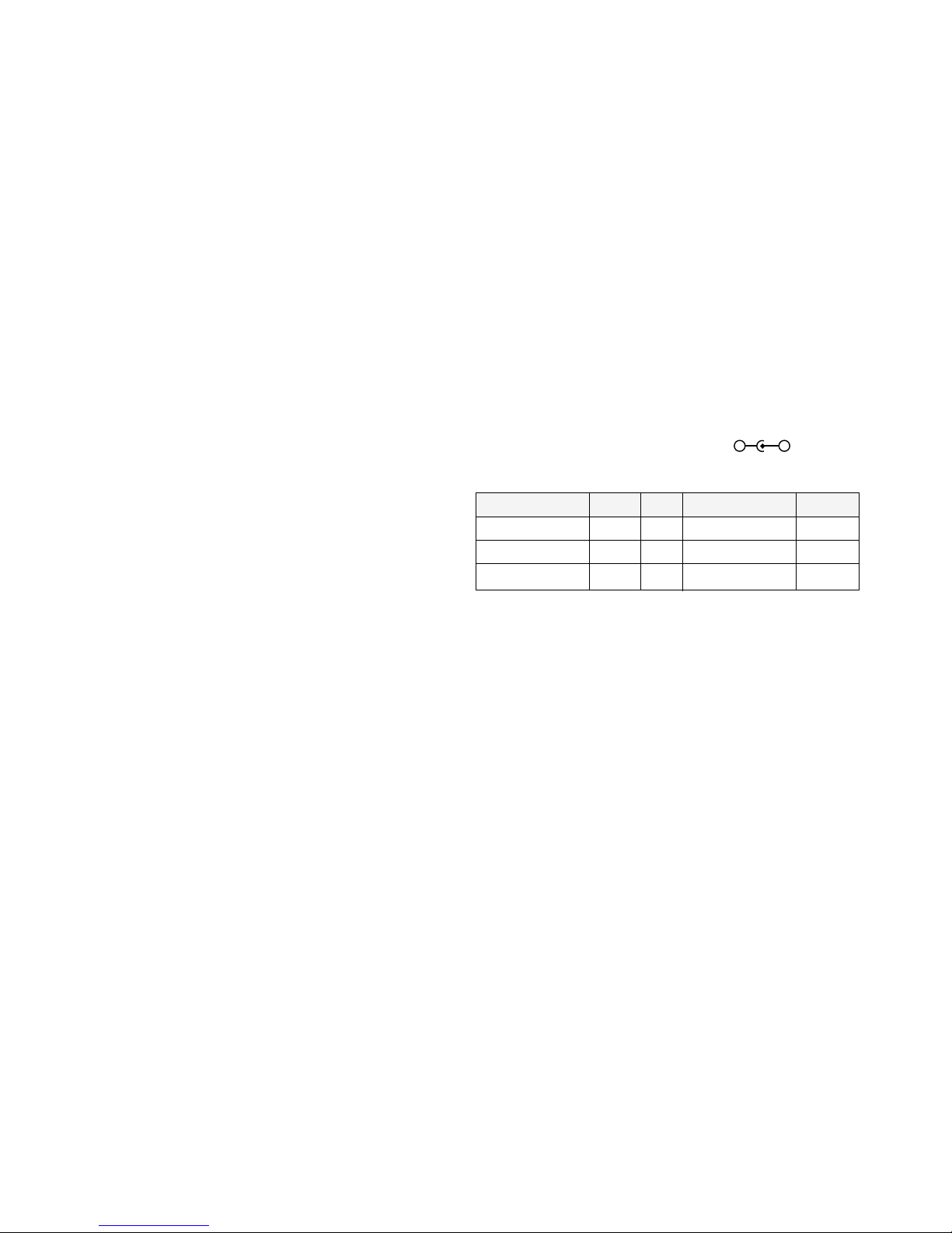
SPECIFICATIONS
-
+
Page 3
WARNING FOR THE SAFETY-RELATED COMPONENT.
• There are some special components used in LCD
monitor that are important for safety. These parts are
marked on the schematic diagram and the
replacement parts list. It is essential that these critical
parts should be replaced with the manufacturer’s
specified parts to prevent electric shock, fire or other
hazard.
• Do not modify original design without obtaining written
permission from Gateway2000 Inc. or you will void the
original parts and labor guarantee.
TAKE CARE DURING HANDLING THE LCD MODULE
WITH BACKLIGHT UNIT.
• Must mount the module using mounting holes arranged
in four corners.
• Do not press on the panel, edge of the frame strongly
or electric shock as this will result in damage to the
screen.
• Do not scratch or press on the panel with any sharp
objects, such as pencil or pen as this may result in
damage to the panel.
• Protect the module from the ESD as it may damage the
electronic circuit (C-MOS).
• Make certain that treatment person’s body are
grounded through wrist band.
• Do not leave the module in high temperature and in
areas of high humidity for a long time.
• The module not be exposed to the direct sunlight.
• Avoid contact with water as it may a short circuit within
the module.
• If the surface of panel become dirty, please wipe it off
with a softmaterial. (Cleaning with a dirty or rough cloth
may damage the panel.)
WARNING
BE CAREFUL ELECTRIC SHOCK !
• If you want to replace with the new backlight (CCFL) or
inverter circuit, must turn off the power button or
disconnect the AC adapter because high voltage
appears at inverter circuit about 650Vrms.
• Handle with care wires or connectors of the inverter
circuit. If the wires are pressed cause short and may
burn or take fire.
- 3 -
PRECAUTION
CAUTION
Please use only a plastic screwdriver to protect yourself
from shock hazard during service operation.
CAUTION
• There is two backlight, must distinguish between
the top (upper) and the bottom (lower), and be
careful of treatment it.
• MTBF (Mean Time Between Failure) of a backlight
is about 10,000 hours.
Top (Upper) Backlight Ass’y
(P/N: 6913TZZ001A)
Bottom (Lower) Backlight Ass’y
(P/N: 6913TZZ001B)
IF BRIGHTNESS OF THE LCD MODULE DARKEN,
REPLACE THE BACKLIGHT ONE OR ALL.
Page 4
- 4 -
VIDEO
SYNC
C
E
D
F
A
B
TIMING CHART
MODE
1
H
(Pixels)
V
(Lines)
Sync
Polarity
_
_
Dot Clock
65MHz
1024
X
768
48.363KHz
60.0Hz
1344
806
1024 320
768
24
38
136
36
160
29
Frequency
Total
Period
(A)
Video
Active
Time
(B)
Blanking
Time
(C)
Sync
Duration
(E)
Back
Porch
(F)
Front
Porch
(D)
Resolution
OPERATING INSTRUCTIONS
ID Label
Power ON/OFF Button
This button is used to turn the monitor on and off.
Power Indicator
This indicator lights up green when the monitor operates
normally; in DPMS (Energy Saving) mode, -stand-by,
suspend, or power off mode-its color changes to orange.
Brightness Control Buttons
Use these buttons for adjusting the brightness.
+
+
Power Input
Socket
DFP
Signal Connector
Front View
Rear View
Page 5
- 5 -
WIRING DIAGRAM
CN1
CN3
J501
CN2
J8-1
J301
J302
J303
J304
CN601
Page 6
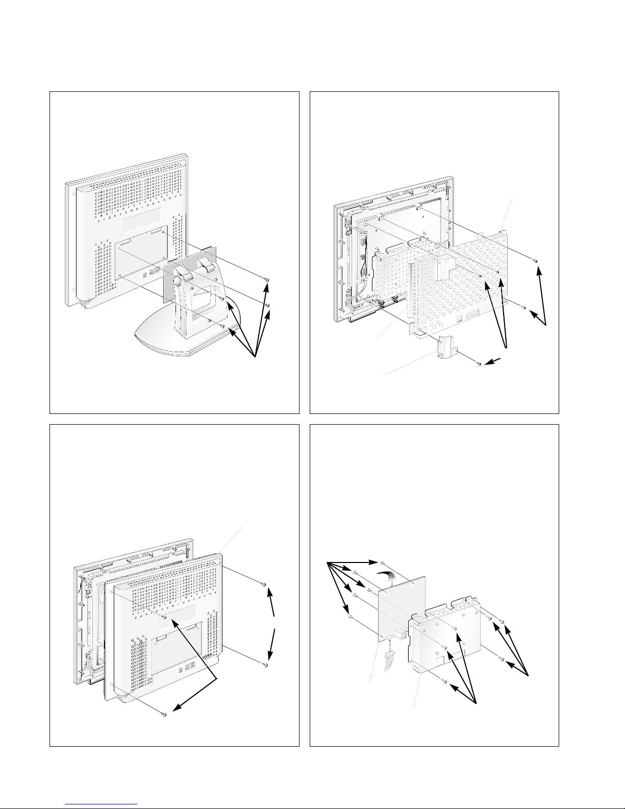
DISASSEMBLY
- 6 -
ⓐ
1. TILT/SWIVEL REMOVAL
①Remove four screws ⓐ.
②Remove the Tilt/swivel.
2. BACK COVER REMOVAL
①Remove four screws ⓐ from the Back Cover.
②Remove the Back Cover.
3. INVERTER CAPS & TOP SHIELD REMOVAL
①Remove five screws ⓐ.
②Remove two Inverter Caps (Upper, Lower).
③Remove the Top Shield.
4. MAIN PCB ASSEMBLY REMOVAL
①Remove six screws ⓐ.
②Disconnect J301 and J501 from the Main PCB.
③Remove the PCB Shield.
④Remove five screws ⓑ.
⑤Remove the Main PCB from the PCB Shield.
ⓐ
ⓐ
ⓐ
ⓐ
ⓐ
ⓑ
ⓐ
Inverter Cap (Upper)
Inverter Cap (Lower)
Main PCB
PCB Shield
Back Cover
Top Shield
J501
J301
Page 7

- 7 -
ⓒ
ⓐ
ⓐ
ⓑ
ⓐ
5. INVERTER, POWER, CONTROL PCB
AND MAIN FRAME REMOVAL
①Remove two screws ⓐ.
②Disconnect CN1 and CN2.
③Remove Inverter PCB.
④Remove two screws ⓑ.
⑤Remove the Power and the CONTROL PCB.
⑥Remove four screws ⓒ.
⑦Remove the Front Cabinet.
6. BACKLIGHT REMOVAL
①Remove two screws ⓐ.
②Remove two Sponge Tapes.
③Remove the Backlight from the LCD Module.
ⓐ
7. LCD MODULE REMOVAL
①Remove four screws ⓐ.
②Divide the LCD Module and the Main Frame.
Bottom (Lower) Backlight Ass’y
Top (Upper) Backlight Ass’y
Front Cabinet
Power PCB
CONTROL PCB
Inverter PCB
LCD Module
LCD Module
Main Frame
Page 8

BLOCK DIAGRAM
Description of Block Diagram
- 8 -
DFP 20Pin
Connector
PanelLink
Connector
EMI Filter
To LCD Module
T
X
0
T
X
1
T
X
2
T
X
C
2
From PC
DPM_det
I2C
Power Connector
From AC/DC
Adapter
DC/DC
Converter
(Max785)
GND
+24V
Inverter
Connecter
To
Inverter
Power switching
(SI4925)
System
Controller
(68HC05BD1)
To key button
Voltage
Regulator
(78M12,05)
+5Vst
+5V
Voltage
Regulator
+5Vmod
+3.3Vcc
+3.3Vcc
+24Vinv
+24Vinv
Inv_onoff
PWM_in
Inv_onoff
PWM_in
P_ctrl
EEPROM
(24C02)
EEPROM
(24C02)
2 2 2
2 2 2 2
System Block Diagram
Block Diagram for Main Logic Board
1.DC/DC Converter
This curcuit supplies stand-by 5V(+5Vst) and regular
5V(+5V) for using MAX785 from AC/DC adapter(+24V).
The +5V voltage supply to power swichng IC(SI4925)
and 3.3V voltage regulator.
The state of power down makes all voltage except
+5Vst down using SHDN pin from system controller
(68HC05BD1).
2. System Controller
This curcuit consists of two EEPROM IC(24C02)
which stores the control data for system and
communicates
DDC(Display Data Channel) and oscillator(X201).
The operating procedures of system controller and its
associated circuit are as follows:
1) The system controller detects frequency of vertical
sync through DFP(Digital Flat Panel) 20 pin
connector.
This controller controls the power swiching
IC(SI4925) by the detection of verticalsync(HVsync).
2) The system controller controls the brightness of
inverter by using the key control button and store
the data to EEPROM(24C02).
3. Power Swiching Circuit
This block supplies +24V(+24Vin) to the inverter for
the backlight voltage of the LCD module and +5V
(+5Vmod) for data control of the LCD module.
4. Signal Transmission
The digital video signals(R,G,B) and clock signals(CLK)
by differencial signals(Tx0,Tx1,Tx2,Txc), are transmitted
to LCD module through EMI filter from PC system which
has digital video card.
LCD Module
Inverter PCB
Main Logic PCB
Button PCB
Power
Supply
Power
Cord
DFP Signal Cable
20Pin
Page 9

- 9 -
NO POWER
(POWER INDICATOR OFF)
TROUBLE IN
U101
TROUBLE IN
AC/DC ADAPTER
CHECK
J101 PIN1
INPUT VOLTAGE
24V ?
NO
YES
YES
YES
YES
YES
YES
YES
TROUBLE IN
J101, J102
CHECK
U50 PIN 1
INPUT VOLTAGE
24V ?
NO
TROUBLE IN
U102, U103
CHECK
5VST VOLTAGE
5V ?
NO
TROUBLE IN
Q101, Q102
CHECK
+5V VOLTAGE
5V ?
NO
TROUBLE IN
U104
CHECK
+3.3V VOLTAGE
3.3V ?
NO
TROUBLE IN
Q403, Q401
CHECK
+24V_INV VOLTAGE
24V ?
NO
TROUBLE IN
Q402, Q401
CHECK
+5V_MOD VOLTAGE
5V ?
NO
TROUBLE-SHOOTING GUIDE
1. NO POWER
Page 10

- 10 -
CHECK PC
or SIGNAL CABLE
CHECK
CN602 PIN 1, 2, 5, 6
11, 12, 15, 16
SIGNAL ?
NO
TROUBLE IN
CMF601, 602, 603, 604
CHECK
CN601 PIN 9, 10, 12, 13,
15, 16, 18, 19
SIGNAL ?
NO
TROUBLE IN
CN601, TMDS CABLE,
LCD MODULE
CHECK
CN601 PIN 20
Vsync ?
NO
TROUBLE IN
U601
CHECK
U201 PIN 28
Vsync ?
NO
REFER TO NO POWER
CHECK
POWER LINE ?
NO
YES
YES
YES
YES
YES
YES
2. NO RASTER
NO RASTER
TROUBLE IN
INVERTER
Page 11

- 11 -
3. TROUBLE IN DPM
CHECK PC
CHECK
CN602 PIN 1, 2, 5, 6
11, 12, 15, 16
SIGNAL ?
NO
TROUBLE IN
DPM MODE
RECHECK PC
& SIGNAL CABLE
TROUBLE IN
LCD MODULE
CHECK
CN601 PIN 20
Vsync ?
NO
TROUBLE IN
U601
CHECK
U201 PIN 28
Vsync ?
NO
TROUBLE IN
U201(MICOM)
CHECK
U201 PIN 12, 15
HIGH ?
NO
YES
YES
YES
YES
Page 12

- 12 -
PRINTED CIRCUIT BOARD
1. MAIN BOARD (Component Side)
2. MAIN BOARD (Solder Side)
Page 13

- 13 -
3. CONTROL BOARD (Component Side)
4. CONTROL BOARD (Solder Side)
5. INTERFACE BOARD (Component Side)
6. INTERFACE BOARD (Solder Side)
Page 14

1
2
3
4
13
14
7
8
9
5
6
A
15
16
10
11
12
EXPLODED VIEW
- 14 - - 15 -
Page 15

- 16 -
EXPLODED VIEW PARTS LIST
Ref. No.
1
2
3
4
5
6
7
8
9
10
11
12
13
14
15
16
A
Part No.
3091TKL005A
6304TLT151B
6633TZA003A
4950TKS072D
4950TKK060A
4950TKK061A
4950TKK047A
3809TKL005A
6871TST085A
332-095C
3043TKK023D
332-105F
6871TMT078A
4950TKK048B
6866TDM001A
6634TBZ004A
3313TL5004A
Description
CABINET ASS’Y, LG501, NO BRAND
LCD MODULE, LGE TFT LCD LM151X1-G 15.1”
INVERTER PCB ASS’Y
MAIN FRAME
INVERT CAP (UP)
INVERT CAP (DOWN)
MAIN SHIELD
BACK COVER ASS’Y
CONTROL BUTTON PCB ASS’Y
SCREW, PZP+3x12
TILT SWIVEL ASS’Y
SCREW, PVS+4x10
MAIN PCB ASS’Y
PCB SHIELD
SIGNAL CABLE
ADAPTER, AC-DC
MAIN TOTAL ASS’Y
Q'ty
1
1
1
1
1
1
1
1
1
4
1
4
1
1
1
1
1
Material
LGC LUPOY GN5001TF
LGC LUPOY GN5001TF
LGC HIPS 60HR
Page 16

REPLACEMENT PARTS LIST
CAUTION:BEFORE REPLACING ANY OF THESE COMPONENTS,
READ CAREFULLY THE SAFETY PRECAUTIONS IN THIS MANUAL.
* NOTE :S SAFETY Mark
AL ALTERNATIVE PARTS
MODEL: Gateway FPD 1500 DATE: 1998 . 9. 20.
*S *AL LOC. NO. PART NO. DESCRIPTION / SPECIFICATION REMARK
C101 0CH8107J611 CAPACITOR, CHIP[AL. ELECTROLYTIC], 100UF 35V M 85STD
C102 0CH7106F621 CAP ACITOR, CHIP[TANTALUM], 10UF 16V M 3528MM TP(-)
C103 0CH3103K516 CAPACITOR, CHIP[CERAMIC LD-LESS HD], 10000PF 50V K B
C104 0CH3104K566 CAPACITOR, CHIP[CERAMIC LD-LESS HD], 0.1UF 50V K X
C105 0CH3224K944 CAPACITOR, CHIP[CERAMIC LD-LESS HD], 0.22UF 50V Z F
C106 0CH3104K566 CAPACITOR, CHIP[CERAMIC LD-LESS HD], 0.1UF 50V K X
C107 0CH3103K516 CAPACITOR, CHIP[CERAMIC LD-LESS HD], 10000PF 50V K B
C108 0CH6102K406 CAPACITOR, CHIP[CERAMIC LD-LESS TC], 1000PF 50V J SL
C109 0CH7227C661 CAPACITOR, CHIP[TANTALUM], 220UF 6.3V M 7343 TP(-)
C110 0CH7107F661 CAPACITOR, CHIP[TANTALUM], 100UF 16V M 7343 TP(-)
C111 0CH3104K566 CAPACITOR, CHIP[CERAMIC LD-LESS HD], 0.1UF 50V K X
C112 0CH3103K516 CAPACITOR, CHIP[CERAMIC LD-LESS HD], 10000PF 50V K B
C113 0CH7476F661 CAPACITOR, CHIP[TANTALUM], 47UF 16V M 7343 TP(-)
C114 0CH3104K566 CAPACITOR, CHIP[CERAMIC LD-LESS HD], 0.1UF 50V K X
C115 0CH3103K516 CAPACITOR, CHIP[CERAMIC LD-LESS HD], 10000PF 50V K B
C116 0CH6102K406 CAPACITOR, CHIP[CERAMIC LD-LESS TC], 1000PF 50V J SL
C117 0CH6221K416 CAPACITOR, CHIP[CERAMIC LD-LESS TC], 220PF 50V J NP0
C118 0CH6221K416 CAPACITOR, CHIP[CERAMIC LD-LESS TC], 220PF 50V J NP0
C119 0CH8107J611 CAPACITOR, CHIP[AL. ELECTROLYTIC], 100UF 35V M 85STD
C120 0CH6101K416 CAPACITOR, CHIP[CERAMIC LD-LESS TC], 100PF 50V J NP0
C121 0CH3104K566 CAPACITOR, CHIP[CERAMIC LD-LESS HD], 0.1UF 50V K X
C123 0CH7106F621 CAP ACITOR, CHIP[TANTALUM], 10UF 16V M 3528MM TP(-)
C124 0CH3103K516 CAPACITOR, CHIP[CERAMIC LD-LESS HD], 10000PF 50V K B
C125 0CH7106F621 CAP ACITOR, CHIP[TANTALUM], 10UF 16V M 3528MM TP(-)
C126 0CH3103K516 CAPACITOR, CHIP[CERAMIC LD-LESS HD], 10000PF 50V K B
C127 0CH8107J611 CAPACITOR, CHIP[AL. ELECTROLYTIC], 100UF 35V M 85STD
C129 0CH8107J611 CAPACITOR, CHIP[AL. ELECTROLYTIC], 100UF 35V M 85STD
C130 0CH3104K566 CAPACITOR, CHIP[CERAMIC LD-LESS HD], 0.1UF 50V K X
C131 0CH3103K516 CAPACITOR, CHIP[CERAMIC LD-LESS HD], 10000PF 50V K B
C201 0CH7226F651 CAP ACITOR, CHIP[TANTALUM], 22UF 16V M 6032 TP(-)
C202 0CH3104K566 CAPACITOR, CHIP[CERAMIC LD-LESS HD], 0.1UF 50V K X
C203 0CH6220K416 CAPACITOR, CHIP[CERAMIC LD-LESS TC], 22PF 50V J NP0
C204 0CH6220K416 CAPACITOR, CHIP[CERAMIC LD-LESS TC], 22PF 50V J NP0
C205 0CH3104K566 CAPACITOR, CHIP[CERAMIC LD-LESS HD], 0.1UF 50V K X
C206 0CH3103K516 CAPACITOR, CHIP[CERAMIC LD-LESS HD], 10000PF 50V K B
C401 0CH8106J611 CAPACITOR, CHIP[AL. ELECTROLYTIC], 10UF 35V M 85STD
C402 0CH3104K566 CAPACITOR, CHIP[CERAMIC LD-LESS HD], 0.1UF 50V K X 2012
- 17 -
MAIN BOARD
CAPACITORs
Page 17

MODEL: Gateway FPD 1500 DATE: 1998 . 9. 20.
*S *AL LOC. NO. PART NO. DESCRIPTION / SPECIFICATION REMARK
C403 0CH8106J611 CAPACITOR, CHIP[AL. ELECTROLYTIC], 10UF 35V M 85STD
C404 0CH3104K566 CAPACITOR, CHIP[CERAMIC LD-LESS HD], 0.1UF 50V K X
C406 0CH7226F651 CAP ACITOR, CHIP[TANTALUM], 22UF 16V M 6032 TP(-)
C407 0CH3103K516 CAPACITOR, CHIP[CERAMIC LD-LESS HD], 10000PF 50V K B
C408 0CH6101K416 CAPACITOR, CHIP[CERAMIC LD-LESS TC], 100PF 50V J NP0
C410 0CH8106J611 CAPACITOR, CHIP[AL. ELECTROLYTIC], 10UF 35V M 85STD
C411 0CH3104K566 CAPACITOR, CHIP[CERAMIC LD-LESS HD], 0.1UF 50V K X
C412 0CH3103K516 CAPACITOR, CHIP[CERAMIC LD-LESS HD], 10000PF 50V K B
C501 0CH6221K416 CAPACITOR, CHIP[CERAMIC LD-LESS TC], 220PF 50V J NP0
C502 0CH6221K416 CAPACITOR, CHIP[CERAMIC LD-LESS TC], 220PF 50V J NP0
C503 0CH6221K416 CAPACITOR, CHIP[CERAMIC LD-LESS TC], 220PF 50V J NP0
C504 0CH6221K416 CAPACITOR, CHIP[CERAMIC LD-LESS TC], 220PF 50V J NP0
C505 0CH6221K416 CAPACITOR, CHIP[CERAMIC LD-LESS TC], 220PF 50V J NP0
C601 0CH3104K566 CAPACITOR, CHIP[CERAMIC LD-LESS HD], 0.1UF 50V K X
CMF601 6140TBZ007C COIL, CHOKE, COMMON-MODE CHOKE,ZCYS51R5-2PAT(TDK)
CMF602 6140TBZ007C COIL, CHOKE, COMMON-MODE CHOKE,ZCYS51R5-2PAT(TDK)
CMF603 6140TBZ007C COIL, CHOKE, COMMON-MODE CHOKE,ZCYS51R5-2PAT(TDK)
CMF604 6140TBZ007C COIL, CHOKE, COMMON-MODE CHOKE,ZCYS51R5-2PAT(TDK)
CN301 366-184F WAFER, 53015-0710 MOLEX 2.0mm R/A
CN501 6602T10001D WAFER, SM10B-SRSS-TB JST 1.0mm R/A
CN601 6602T11001A WAFER, FI-TWE21P-VF JAE 1.0mm S/T
CN602 6602T20007B WAFER, 87089-2016 MOLEX 2.0MM BOARD
D101 0DS181009AA DIODE, SWITCHING, KDS181 TP KEC SOT-23 80V 300MA 2A
D102 0DR190309AA DIODE, RECTIFIER, MBRS190T3 TP MOTOROLA 403A-03 90V
L101 6210TCT002C CORE (CIRC), BEAD, HF50ACC575018-T TDK , CHIP BEAD,LCD
L102 6140TBZ016A COIL, CHOKE, DR10*5 22UH 0.45MM 20.5T LG501
L103 6200TEZ007A FILTER(CIRC), CAPACITOR, STC-B SERIES(104B) NIIGATA(FILMAC)
L104 6140TBZ016A COIL, CHOKE, DR10*5 22UH 0.45MM 20.5T LG501
L105 6210TCE001G CORE (CIRC), BEAD, HH-1M3216-501 CERATEC 3216MM R/TP
L106 6210TCE001G CORE (CIRC), BEAD, HH-1M3216-501 CERATEC 3216MM R/TP
L401 6200TEZ007A FILTER(CIRC), CAPACITOR, STC-B SERIES(104B) NIIGATA(FILMAC)
L501 6210TCE001C CORE (CIRC), BEAD, HB-1T3216-500JT CERATEC , CHIP-BEAD
L502 6210TCT002B CORE (CIRC), BEAD, ACB2012M-300-T TDK , CHIP BEAD,LCD
L503 6210TCT002B CORE (CIRC), BEAD, ACB2012M-300-T TDK , CHIP BEAD,LCD
U101 0IMX785000B IC, MAXIM, MAX785CAI 28P,SSOP TP DUAL OUTPWRSUPPLY
U102 0ISS781200J IC, SAMSUNG ELECTRONICS,KA78M12R 3P,D-PAK TP VOL.
U103 0ISS780500H IC, SAMSUNG ELECTRONICS, KA78M05-R 3P,D-PAK TP 5V 0.5A
U104 0IRH033200A IC, ROHM, BA033FP-E2 MOLD-3 TP REGULATOR
U201 0IZZTSZ011A IC [HYBRID], 28P DIP BK, MC68HC705BD1A, LG501
- 18 -
DIODEs
COILs & COREs
ICs
Page 18

MODEL: Gateway FPD 1500 DATE: 1998 . 9. 20.
*S *AL LOC. NO. PART NO. DESCRIPTION / SPECIFICATION REMARK
U202 0IMP240200A IC, MICRO CHIP TECHNOLOGY, 24LC02BT/SN 3.3K/ TP
U203 0IMP240200A IC, MICRO CHIP TECHNOLOGY, 24LC02BT/SN 3.3K/ TP
U601 0IMO741420B IC, MOTOROLA, MC74HCT14ADR2 14P,SOIC TP LEVEL
Q101 0TF993609AA FET, SI9936DY TP TEMIC 30V 5A SO-8
Q102 0TF941009AA FET, SI9410DY TP TEMIC 30V 7A SO-8
Q401 0TF492509AA FET, SI4925DY TP TEMIC 30V 6.1A SO-8
Q402 0TR162309CA TRANSISTOR, KSC1623 TP SAMSUNG SOT23 NPN EPI
Q403 0TR162309CA TRANSISTOR, KSC1623 TP SAMSUNG SOT23 NPN EP
R101 0RH1003D422 RESISTOR, CHIP, 100K 1/10W 1% D R/TP
R102 0RH0000D622 RESISTOR, CHIP, 0 1/10W P-TYPE TAPPING
R103 0RH4701D622 RESISTOR, CHIP, 4.7K 1/10W 5 D.R/TP
R104 0RHZTJZ001B RESISTOR, CHIP, 0.025 OHM 1 W 2% 2512 R/TP ,IRC
R201 0RH1000D622 RESISTOR, CHIP, 100 1/10W 5 D.R/TP
R202 0RH4701D622 RESISTOR, CHIP, 4.7K 1/10W 5 D.R/TP
R203 0RH4701D622 RESISTOR, CHIP, 4.7K 1/10W 5 D.R/TP
R204 0RH0000D622 RESISTOR, CHIP, 0 1/10W P-TYPE TAPPING
R205 0RH0000D622 RESISTOR, CHIP, 0 1/10W P-TYPE TAPPING
R206 0RH0000D622 RESISTOR, CHIP, 0 1/10W P-TYPE TAPPING
R207 0RH0000D622 RESISTOR, CHIP, 0 1/10W P-TYPE TAPPING
R208 0RH3300D622 RESISTOR, CHIP, 330 1/10W 5 D.R/TP
R209 0RH3300D622 RESISTOR, CHIP, 330 1/10W 5 D.R/TP
R210 0RH4701D622 RESISTOR, CHIP, 4.7K 1/10W 5 D.R/TP
R211 0RH4701D622 RESISTOR, CHIP, 4.7K 1/10W 5 D.R/TP
R212 0RH1000D622 RESISTOR, CHIP, 100 1/10W 5 D.R/TP
R213 0RH1000D622 RESISTOR, CHIP, 100 1/10W 5 D.R/TP
R214 0RH4701D622 RESISTOR, CHIP, 4.7K 1/10W 5 D.R/TP
R401 0RH6802D622 RESISTOR, CHIP, 68K 1/10W 5 D.R/TP
R402 0RH1002D622 RESISTOR, CHIP, 10K 1/10W 5 D.R/TP
R403 0RH1002D622 RESISTOR, CHIP, 10K 1/10W 5 D.R/TP
R404 0RH1002D622 RESISTOR, CHIP, 10K 1/10W 5 D.R/TP
R405 0RH6802D622 RESISTOR, CHIP, 68K 1/10W 5 D.R/TP
R406 0RH6802D622 RESISTOR, CHIP, 68K 1/10W 5 D.R/TP
R407 0RH1002D622 RESISTOR, CHIP, 10K 1/10W 5 D.R/TP
R408 0RH1002D622 RESISTOR, CHIP, 10K 1/10W 5 D.R/TP
R603 0RH1002D622 RESISTOR, CHIP, 10K 1/10W 5 D.R/TP
R604 0RH1002D622 RESISTOR, CHIP, 10K 1/10W 5 D.R/TP
R605 0RH1002D622 RESISTOR, CHIP, 10K 1/10W 5 D.R/TP
R606 0RH5100D622 RESISTOR, CHIP, 510 1/10W 5 D.R/TP
R607 0RH5100D622 RESISTOR, CHIP, 510 1/10W 5 D.R/TP
R608 0RH5100D622 RESISTOR, CHIP, 510 1/10W 5 D.R/TP
R609 0RH5100D622 RESISTOR, CHIP, 510 1/10W 5 D.R/TP
- 19 -
RESISTORs
TRANAITORs
Page 19

MODEL: Gateway FPD 1500 DATE: 1998 . 9. 20.
*S *AL LOC. NO. PART NO. DESCRIPTION / SPECIFICATION REMARK
X201 6202TST001B CRYSTAL, SX-1 SUNNY ,SMD, 4.0MHZ ,30PPM, 18PF, TP
CN302 366-184F WAFER, 53015-0710 MOLEX 2.0mm R/A
CN303 366-184D WAFER, 53015-0510 MOLEX 2.0mm R/A
CN304 366-183D WAFER, 53014-0510 MOLEX 2.0mm S/T
LD301 0DL571300AA LED, SPR571MVW3 TP ROHM GREEN/RED 10,10MCD
R301 0RD1801Q609 RESISTOR, FIXED CARBON FILM, 1.80K 1/4W(3 5% TA52
R302 0RD4700Q609 RESISTOR, FIXED CARBON FILM, 470 OHM 1/4 W (3.4) 5%
R303 0RD1001Q609 RESISTOR, FIXED CARBON FILM, 1K 1/4W(3 5% TA52
S301 140-058E SWITCH, TACT, SKHV10910B LGEC NON 12V 20A HORIZENTAL
S302 140-058E SWITCH, TACT, SKHV10910B LGEC NON 12V 20A HORIZENTAL
S303 140-058E SWITCH, TACT, SKHV10910B LGEC NON 12V 20A HORIZENTAL
ZD301 0DZ560009CE DIODE, ZENER, MTZJ5.6B TP ROHM-K DO34 500MW 5.6V 5MA
J101 6612TAH002A JACK,AC/DC POWER, DC-001 UNITOP DC-001 2.0MM (UNITOP)
J102 6602T25007A WAFER, GC250-3P-LS-SO LGC 2.5mm R/A
J603 6602T20007A WAFER, 87264-2050 MOLEX 2.0MM BOARD
J604 6630TGA002A CONNECTOR (CIRC), D-SUB, 10220-55F3JL 3M 20PIN 1.27MM
LCD 6304TLT151B LCD, LGE TFT LCD LM151X1-G 15.1” 1024X768
ADAPTER
6634TBZ004A ADAPTER,AC-DC, PSCV450106A SAMSUNG 100V 24V 1.875A
INVERTER
6633TZA003A INVERTER ASSY, SAMSUNG LG1501 FOR 15.1” LCD MNT
or
INVERTER
6633TZA001A INVERTER ASSY, AMBIT REV.1, (UO4.32.C.00) LCD
P/CORD 174-206F POWER CORD, UL/CSA 1830MM WALL IVORY
or P/CORD
174-240A & 174-240A
POWER CORD, WALL OUT, 6FT, BK, FOR JAPAN ONLY
S/CABLE 6866TDM001A SIGNAL CABLE, UL20276 DT 2000MM COOL GRAY 3C
M-INVERTER
6631T10001C CONNECTOR ASSY, 10P H-H 130MM UL 1571 28
M-MODULE
6631T11006C CONNECTOR ASSY, 21P H-H 220MM UL20276SB10P+2C
M-CTRL 6631T20005E CONNECTOR ASSY, 7P H-H 60MM UL1061 AWG 26 TW
C-
POWER
6631T20005B CONNECTOR ASSY, 5P,H-H,L60,UL1061 26
- 20 -
MISCELLANEOUS
CONTROL BOARD
INTERFACE BOARD
OTHERs
Page 20

PIN NAME FUNCTION
1 CS3 Current-sense input for +3.3V; +100mV = current limit level referenced to FB3.
2 SS3 Soft-start input for +3.3V. Ramp time to full current limit is 1ms/nF of capacitance to GND.
3 ON3 ON/
OFF
control input disables the +3.3V PWM. Tie directly to VL for automatic start-up.
4 D1 #1 level-translator/comparator noninverting input, threshold = +1.650V. Controls Q1. Tie to GND if unused.
5 D2 #2 level-translator/comparator noninverting input (see D1)
6 VH External positive supply-voltage input for the level translators/comparators
7Q2
#2 level-translator/comparator output. Sources 20µA from VH when D2 is high. Sinks 500µA to GND
when D2 is low, even with VH = 0V.
8 Q1 #1 level translator/comparator output (see Q2)
9 GND Low-current analog ground
10 REF 3.3V reference output. Sources up to 5mA for external loads. Bypass to GND with 1µF/mA of load or
0.22µF minimum.
11 SYNC
Oscillator control/synchronization input. Connect to VL or GND for 200kHz; connect to REF for
300kHz. For external clock synchronization in the 240kHz to 350kHz range, a high-to-low transition
causes a new cycle to start.
12
SHDN
Shutdown control input, active low. Tie to VL for automatic start-up. The 5V VL supply stays active in
shutdown, but all other circuitry is disabled. Do not force
SHDN
higher than VL + 0.3V.
13 ON5 ON/
OFF
control input disables the +5V PWM supply. Tie to VL for automatic start-up.
14 SS5 Soft-start control input for +5V. Ramp time to full current limit is 1ms/nF of capacitance to GND.
15 CS5 Current-sense input for +5V; +100mV = current-limit level referenced to FB5.
16 DH5 Gate-drive output for the +5V high-side MOSFET
17 LX5 Inductor connection for the +5V supply
18 BST5 Boost capacitor connection for the +5V supply (0.1µF)
19 DL5 Gate-drive output for the +5V low-side MOSFET
20 PGND Power ground
21 FB5 Feedback and current-sense input for the +5V PWM
22 VL 5V logic supply voltage for internal circuitry. VL is always on and can source 5mA for external loads.
23 V+ Supply voltage input from battery, 5.5V to 30V
24 DL3 Gate-drive output for the +3.3V low-side MOSFET
25 BST3 Boost capacitor connection for the +3.3V supply (0.1µF)
26 LX3 Inductor connection for the +3.3V supply
27 DH3 Gate-drive output for the +3.3V high-side MOSFET
28 FB3 Feedback and current-sense input for the +5V PWM
PIN CONFIGURATION
28
27
26
25
24
23
22
21
1
2
3
4
5
6
7
8
FB3
DH3
LX3
BST3
D1
ON3
SS3
CS3
DL3
V+
VL
FB5
Q1
Q2
VH
D2
20
19
18
17
9
10
11
12
PGND
DL5
BST5
LX5
SHDN
SYNC
REF
GND
16
15
13
14
DH5
CS5
SS5
ON5
MAX785 Dual-Output Power-Supply Controller
28
1
PIN CONFIGURATION
Page 21

P
+5V LDO
LINEAR
REGULATOR
V+
VL
REF
SHDN
GND
+3.3V
REFERENCE
ON
3.3V
5V
4V
2.8V
SYNC
300kHz/200kHz
OSCILLATOR
ON
STANDBY
4.5V
FAULT
ON
3.3V
PWM
CONTROLLER
(SEE FIG. 3)
FB3
CS3
BST3
DH3
LX3
DL3
SS3
FB5
CS5
BST5
DH5
LX5
DL5
SS5
PGND
ON3
5V
PWM
CONTROLLER
(SEE FIG. 3)
ON
D1
D2
1.65V
1.65V
ON5
VH
Q1
Q2
BLOCK DIAGRAM FOR MAX785
Page 22

PA1/PWM9
PA0/PWM8
PA2/PWM10
PB5*/PWM5*
PC2/CLAMP
PB3/PWM3**
PC5/AD0
PC3/HSYNCO
PC4/VSYNCO
PB4*/PWM4*
VSYNC
HSYNC
PB1/PWM1**
PB2/PWM2**
MC68HC(7)05BD1A
28-PIN DIP
1
2
3
4
5
6
7
8
9
10
11
12
13
14
28
27
26
25
24
23
22
21
20
19
18
17
16
15
XTAL
PA5/PWM13
PA6/PWM14
PA4/PWM12
PA7/PWM15
EXTAL
IRQ/VPP
VDD
VSS
RESET
SDA/PC0/PWM6***
SCL/PC1/PWM7***
PB0/PWM0**
PA3/PWM11
28
MC68HC705BD1A HCMOS Microcontroller
1
PIN CONFIGURATION
BLOCK DIAGRAM
PA0/PWM8
PA1/PWM9
PA2/PWM10
PA3/PWM11
PA4/PWM12
PA5/PWM13
PA6/PWM14
PA7/PWM15
SDA/PC0/PWM6***
SCL/PC1/PWM7***
PC2/CLAMP
PC3/HSYNCO
PC4/VSYNCO
PC5/AD0
PORT
A REG
DDC12AB/
PORT
C REG
DATA
DIR
REG
IIC
DATA
DIR
REG
EXTALXTAL
OSCILLATOR
AND DIVIDE
BY 2
CPU CONTROL
68HC05 CPU
CPU REGISTERS
COND CODE REG 1 1 1 I N Z CH
3.75K/7.75K bytes
for HC05BD1A
(7.75K bytes for
HC705BD1A)
000 1100000
PROGRAM COUNTER
ROM
VDD
VSS
RESET IRQ/VPP
CORE
TIMER
(COP)
ALU
ACCUM
INDEX REG
STK PTR
128/256 bytes
(256 bytes for
HC705BD1A)
RAM
Pulse
Width
Modulation
(PWM)
6-bit ADC
SYNC
PROCESSOR
PB0/PWM0**
PB1/PWM1**
PB2/PWM2**
PB3/PWM3**
PB4*/PWM4*
PB5*/PWM5*
PORT B REG / DIR REG
HSYNC
VSYNC
Page 23

MC54/74HC14A Hex Schmitt-Trigger Inverter
1314 12 11 10 9 8
21 34567
VCCA6 Y6 A5 Y5 A4 Y4
A1 Y1 A2 Y2 A3 Y3 GND
I/O
Control
Logic
Memory
Control
Logic
XDEC
HV Generator
EEPROM
Array
Write Protect
Circuitry
YDEC
Vcc
Vss
SENSE AMP
R/W CONTROL
SDA
SCL
A0 A1 A2
WP
OUT
Reference Voltage
Vcc
1
2
3
GND
FUNCTION TABLE
14
1
PIN CONFIGURATION
24LC02 2K 2.5V I2C™ Serial EEPROM
Inputs
A
L
H
Outputs
Y
H
L
1
3
A2
5
A3
9
A4
11
A5
13
A6
BLOCK DIAGRAM
10
12
2
Y1A1
4
Y2
6
Y3
Y = A
8
Y4
Pin 14 = V
Pin 7 = GND
Y5
Y6
CC
8
1
A0
A1
A2
Vss
1
2
3
4
24LC024
Vcc
8
WP
7
SCL
6
SDA
5
PIN CONFIGURATION
BA033FP Low Saturation Voltage type 3-terminal Regulator
1
2
3
1. Vcc
2. GND
3. OUTPUT
BLOCK DIAGRAM
BLOCK DIAGRAM
- 24 -
Page 24

- 25 -
SI4925DY Dual P-Channel 30-V (D-S) Rated MOSFET
SI9410DY N-Channel Enhancement-Mode MOSFET
S
1
G
1
D1D
1
S
2
G
2
D2D
2
PIN CONFIGURATION BLOCK DIAGRAM
PIN CONFIGURATION BLOCK DIAGRAM
SI9936DY N-Channel Enhancement-Mode MOSFET
1
8
D
D
D
G
S S
D
1
8
BLOCK DIAGRAM
D
6
1
4
R1
R1
3
2
LD=4nH
DBDDY
LS=6nH
LG=6nH
CGD
DMAX DMIN
CGS
RG=6Ω
G
S
1
8
S
1
1
G
2
1
S
3
2
G
4
2
D
8
1
D
7
1
D
6
2
D
5
2
N/C
1
2
S
3
S
4
G
8
D
7
D
6
D
5
D
Page 25

PARTSTYPE
PARTSTYPE
KDS181
MBRS190T3
12
3
- 26 -
KA78M05R
KA78M12R
1. INPUT
2. GND
3. OUTPUT
1. CATHODE 1
2. CATHODE 2
3. ANODE
1
3
2
1
3
2
KSC1623
1. BASE
2. EMITTER
3. COLLECTOR
2
3
1
1
2
1
2
0CH7106F621
10uF/16V
0CH7107F661
100uF/10V
0CH7226F651
22uF/16V
0CH7227F661
220uF/6.3V
0CH7476F661
47uF/10V
_
+
Regulator
Schottky Diode
Diode
Transistor
Tantalum Capacitor
Page 26

 Loading...