Fairchild Semiconductor H11F3, H11F2, H11F1 Datasheet

• ≥
≤
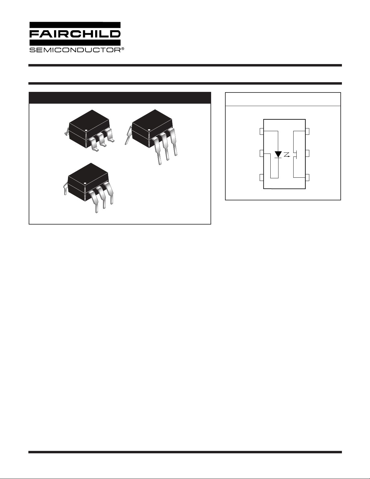
PHOTO FET OPTOCOUPLERS
H11F1 H11F2 H11F3
PACKAGE
ANODE
6
1
6
CATHODE
SCHEMATIC
1
2
OUTPUT
6
TERM.
5
1
OUTPUT
3
4
TERM.
6
1
DESCRIPTION
The H11F series consists of a Gallium-Aluminum-Arsenide IRED emitting diode coupled to a symmetrical bilateral silicon photodetector. The detector is electrically isolated from the input and performs like an ideal isolated FET designed for distortion-free
control of low level AC and DC analog signals. The H11F series devices are mounted in dual in-line packages.
FEATURES
As a remote variable resistor
• ≤ 100 Ω to ≥ 300 M Ω
99.9% linearity
• ≤ 15 pF shunt capacitance
• ≥ 100 G Ω I/O isolation resistance
As an analog switch
• Extremely low offset voltage
• 60 V
• No charge injection or latch-up
•t
on
• UL recognized (File #E90700)
• VDE recognized (File #E94766)
– Ordering option ‘300’ (e.g. H11F1.300)
signal capability
pk-pk
, t
15 µS
off
APPLICATIONS
As a variable resistor –
• Isolated variable attenuator
• Automatic gain control
• Active filter fine tuning/band switching
As an analog switch –
• Isolated sample and hold circuit
• Multiplexed, optically isolated A/D conversion
© 2002 Fairchild Semiconductor Corporation
Page 1 of 9
6/24/02

PHOTO FET OPTOCOUPLERS
H11F1 H11F2 H11F3
Absolute Maximum Ratings
Parameter Symbol Device Value Units
TOTAL DEVICE
Storage Temperature T
Operating Temperature T
Lead Solder Temperature T
EMITTER
Continuous Forward Current I
Reverse Voltage V
Forward Current - Peak (10 µs pulse, 1% duty cycle) I
LED Power Dissipation 25°C Ambient
Derate Linearly From 25°C 1.33 mW/°C
DETECTOR
Detector Power Dissipation @ 25°C
Derate linearly from 25°C 4.0 mW/°C
Breakdown Voltage (either polarity) BV
Continuous Detector Current (either polarity) I
ELECTRICAL CHARACTERISTICS
(T
= 25°C unless otherwise specified)
A
STG
OPR
SOL
F
R
F(pk)
P
D
P
D
4-6
4-6
(T
= 25°C Unless otherwise specified.)
A
All -55 to +150 °C
All -55 to +100 °C
All 260 for 10 sec °C
All 60 mA
All 5 V
All 1 A
All
All
100 mW
300 mW
H11F1, H11F2 ±30 V
H11F3 ±15 V
All ±100 mA
INDIVIDUAL COMPONENT CHARACTERISTICS
Parameter Test Conditions Symbol Device Min Typ* Max Unit
EMITTER
Input Forward Voltage I
Reverse Leakage Current V
Capacitance V = 0 V, f = 1.0 MHz C
OUTPUT DETECTOR
Breakdown Voltage
Either Polarity
Off-State Dark Current
V
4-6
Off-State Resistance V
Capacitance V
© 2002 Fairchild Semiconductor Corporation
4-6
= 16 mA V
F
= 5 V I
R
I
= 10µA, I
4-6
V
= 15 V, I
4-6
= 15 V, I
= 15 V, I
4-6
= 15 V, I
= 0 BV
F
= 0
F
= 0, T
F
= 100°C All 50 µA
A
= 0 R
F
= 0, f = 1MHz C
F
Page 2 of 9
F
R
J
All 1.3 1.75 V
All 10 µA
All 50 pF
H11F1, H11F2 30
4-6
I
4-6
4-6
4-6
H11F3 15
All 50 nA
All 300 M Ω
All 15 pF
6/24/02
V

Ω
Ω
Ω
PHOTO FET OPTOCOUPLERS
H11F1 H11F2 H11F3
ISOLATION CHARACTERISTICS
Parameter Test Conditions Symbol Min Typ* Max Units
Input-Output Isolation Voltage f = 60Hz, t = 1 min. V
Isolation Resistance V
Isolation Capacitance V
TRANSFER CHARACTERISTICS
= 500 VDC R
I-O
= 0, f = 1.0 MHz C
I-O
(T
= 25°C Unless otherwise specified.)
A
ISO
ISO
ISO
5300 Vac (rms)
11
10
2pF
DC Characteristics Test Conditions Symbol Device Min Typ* Max Units
H11F1 200
On-State Resistance I
= 16 mA, I
F
= 100 µA R
4-6
4-6
H11F2 330
H11F3 470
H11F1 200
On-State Resistance I
= 16 mA, I
F
= 100 µA R
6-4
6-4
H11F2 330
H11F3 470
Resistance, non-linearity
and assymetry
= 16mA, I
I
F
= 25 µA RMS,
4-6
f = 1kHz
All 0.1 %
AC Characteristics Test Conditions Symbol Device Min Typ* Max Units
Turn-On Time R
Turn-Off Time R
= 50 Ω , I
L
= 50 Ω , I
L
= 16mA, V
F
= 16mA, V
F
= 5V t
4-6
= 5V t
4-6
on
off
All 25 µS
All 25 µS
© 2002 Fairchild Semiconductor Corporation
Page 3 of 9
6/24/02
 Loading...