

Page 1
D&M Holdings lnc.
e
Copyright 2010 D&M Holdings Inc. All rights reserved.
WARNING: Violators will be prosecuted to the maximum extent possible.
Ver. 5
●
For purposes of improvement, specifications and design are subject to change without notice.
●
Please use this service manual with referring to the operating instructions without fail.
●
Some illustrations using in this service manual are slightly different from the actual set.
Please refer to the
MODIFICATION NOTICE.
SERVICE MANUAL
MODEL JP E3 E2 EK E2A E1C E1K EUT
DRA-F107
DRA-F107DAB
AM-FM STEREO RECEIVER
3
3
S0089-1V05DM/DG1007
Page 2
Please heed the points listed below during servicing and inspection.
SAFETY PRECAUTIONS
The following check should be performed for the continued protection of the customer and service technician.
LEAKAGE CURRENT CHECK
Before returning the unit to the customer, make sure you make either (1) a leakage current check or (2) a line to chassis
resistance check. If the leakage current exceeds 0.5 milliamps, or if the resistance from chassis to either side of the
power cord is less than 460 kohms, the unit is defective.
CAUTION
CAUTION
◎ Heed the cautions!
Spots requiring particular attention when servicing, such
as the cabinet, parts, chassis, etc., have cautions indicated
on labels or seals. Be sure to heed these cautions and the
cautions indicated in the handling instructions.
◎ Caution concerning electric shock!
(1) An AC voltage is impressed on this set, so touching in-
ternal metal parts when the set is energized could
cause electric shock. Take care to avoid electric shock,
by for example using an isolating transformer and
gloves when servicing while the set is energized, unplugging the power cord when replacing parts, etc.
(2)There are high voltage parts inside. Handle with extra
care when the set is energized.
◎ Caution concerning disassembly and
assembly!
Though great care is taken when manufacturing parts from
sheet metal, there may in some rare cases be burrs on the
edges of parts which could cause injury if fingers are
moved across them. Use gloves to protect your hands.
◎ Only use designated parts!
The set's parts have specific safety properties (fire resistance, voltage resistance, etc.). For replacement parts, be
sure to use parts which have the same properties. In particular, for the important safety parts that are marked z on
wiring diagrams and parts lists, be sure to use the designated parts.
◎ Be sure to mount parts and arrange
the wires as they were originally!
For safety reasons, some parts use tape, tubes or other insulating materials, and some parts are mounted away from
the surface of printed circuit boards. Care is also taken with
the positions of the wires inside and clamps are used to
keep wires away from heating and high voltage parts, so
be sure to set everything back as it was originally.
◎ Inspect for safety after servicing!
Check that all screws, parts and wires removed or disconnected for servicing have been put back in their original positions, inspect that no parts around the area that has been
serviced have been negatively affected, conduct an insulation check on the external metal connectors and between
the blades of the power plug, and otherwise check that
safety is ensured.
(Insulation check procedure)
Unplug the power cord from the power outlet, disconnect
the antenna, plugs, etc., and turn the power switch on. Using a 500V insulation resistance tester, check that the insulation resistance between the terminals of the power
plug and the externally exposed metal parts (antenna terminal, headphones terminal, microphone terminal, input
terminal, etc.) is 1MΩ or greater. If it is less, the set must
be inspected and repaired.
Concerning important safety
parts
Many of the electric and structural parts used in the set
have special safety properties. In most cases these properties are difficult to distinguish by sight, and using replacement parts with higher ratings (rated power and
withstand voltage) does not necessarily guarantee that
safety performance will be preserved. Parts with safety
properties are indicated as shown below on the wiring diagrams and parts lists is this service manual. Be sure to replace them with parts with the designated part number.
(1) Schematic diagrams ... Indicated by the z mark.
(2) Parts lists ... Indicated by the z mark.
Using parts other than the designated
parts could result in electric shock, fires or
other dangerous situations.
DRA-F107 / DRA-F107DAB
2
Page 3
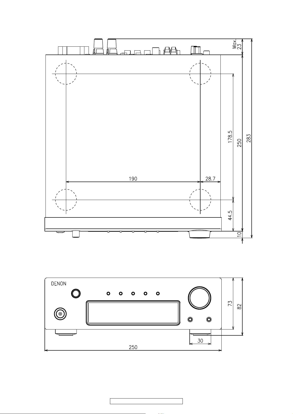
DIMENSION
3
DRA-F107 / DRA-F107DAB
Page 4
WIRE ARRANGEMENT
Front Panel side
Back Panel side
If wire bundles are untied or moved to perform adjustment or parts replacement etc.,be sure to rearrange them neatly as
they were originally bundled or placed afterward.
Otherwise, incorrect arrangement can be a cause of noise generation.
Wire arrangement viewed from the top
4
DRA-F107 / DRA-F107DAB
Page 5
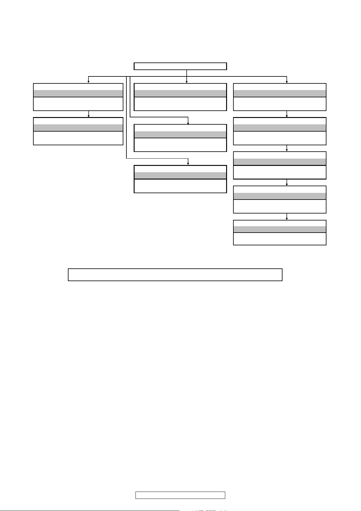
DISASSEMBLY
TOP COVER
FRONT PANEL ASSY AMP PCB REAR PANEL
Refer to "EXPLODED VIEW" Refer to "EXPLODED VIEW" Refer to "EXPLODED VIEW"
FRONT PCB AMP PCB REAR PANEL
(Ref. No. of EXPLODED VIEW : C2) (Ref. No. of EXPLODED VIEW : C7) (Ref. No. of EXPLODED VIEW : M14)
SMPS PCB MAIN PCB
Refer to "EXPLODED VIEW" UPDATE PCB Refer to "EXPLODED VIEW"
SMPS PCB Refer to "EXPLODED VIEW" MAIN PCB
(Ref. No. of EXPLODED VIEW : C3) UPDATE PCB (Ref. No. of EXPLODED VIEW : C8)
(Ref. No. of EXPLODED VIEW : C13)
POWER PCB
Refer to "EXPLODED VIEW"
TUNER PACK POWER PCB
Refer to "EXPLODED VIEW" (Ref. No. of EXPLODED VIEW : C6)
TUNER PACK
(Ref. No. of EXPLODED VIEW : C12)
PHONO PCB
Refer to "EXPLODED VIEW"
PHONO PCB
(Ref. No. of EXPLODED VIEW : C11)
DAB PCB
Refer to "EXPLODED VIEW"
DAB PCB
(Ref. No. of EXPLODED VIEW : C9
Please refer to "EXPLODED VIEW" for the disassembly method of each PCB.
• Disassemble in order of the arrow of the figure of following flow.
• In the case of the re-assembling, assemble it in order of the reverse of the following flow.
5
DRA-F107 / DRA-F107DAB
Page 6

CAUTION IN SERVICING
Note:・ All user settings will be lost and this factory setting will be recovered when this initialization mode.
So make sure to m+emorize your setting for restoring after the initialization.
Initializing DRA-F107/DRA-F107DAB
DRA-F107/DRA-F107DAB initialization should be performed when the μcom, and peripheral parts of μcom are replaced.
1. Switch off the unit and remove the AC cord from the wall outlet.
2. Hold the following the 0 button and the AUTO PRESET button, and plug the AC cord into the outlet. d
6
DRA-F107 / DRA-F107DAB
Page 7
SPECIAL MODECD TEST MODE
DRA VER
D
DOCK
RA VER
VER + +++
No Button name Function Display
S1.1
・
Plug AC cord into power outlet while pressing
the ON/STANDBY button and the SDB/
TONE button same time on Main Unit.
・The Version number of MPU is displayed.
・MUTING ON
・
Unplug AC cord to clear this mode.
S1.2
※ When the iPod Dock is connected
・ Plug AC cord into power outlet while pressing
the ON/STANDBY button and the SDB/
TONE button same time on Main Unit.
・The Version number of MPU is displayed.
・MUTING ON
・
Unplug AC cord to clear this mode.
・ Plug AC cord into power outlet while pressing
the ON/STANDBY button and the AUTO
PRESET button same time on Main Unit.
・All segment of FLD is turning on and off every
one second .
・MUTING ON.
・Unplug AC cord to clear this mode.
***** :The version number of Main MPU
***** :The version number of MPU
++++ :The version number of iPod Dock
・All segment turn on and off.
S1
S1
S2
Versi on No.
Display Mode
Versi on No.
Display Mode
VFD checking
mode
EEPROM
S3
testing Mode
Cold start mode
S4
(Initialization)
・Plug AC cord into power outlet while pressing
the ON/STANDBY button and the TUNER
button same time on Main Unit.
・ON / STANDBY LED lighted ORANGE (The
test is started).
・MUTING ON.
・When power LED lighted Green, this
EEPROM test was OK.
・When power LED lighted RED, this EEPROM
test was NG.
・Unplug AC cord to clear this mode.
・Plug AC cord into power outlet while pressing
the AUTO PRESET button and the
same time on Main Unit.
・The system is reset.
- source : CD/USB
- SDB : OFF
- BASS : 0
- TREBLE : 0
- BALANCE : CENTER
- DIMMER : 100%
- VOLUME : 0
- Preset Frequency of TUNER:
All 0
- Main Unit
- CLOCK : 00:00(Flashing)
- TIMER(EVERYDAY/ONCE):
Timer Function : CD
Timer start time : 0:00 (AM12:00 : E3)
Timer stop time : 0:00 (AM12:00 : E3)
・The system is reset, and once this is com-
pleted the unit is set to the normal mode.
0/1 button:
:
-/+ button for PRESET
AM12:00(Flashing)(E3)
0 button
7
DRA-F107 / DRA-F107DAB
Page 8
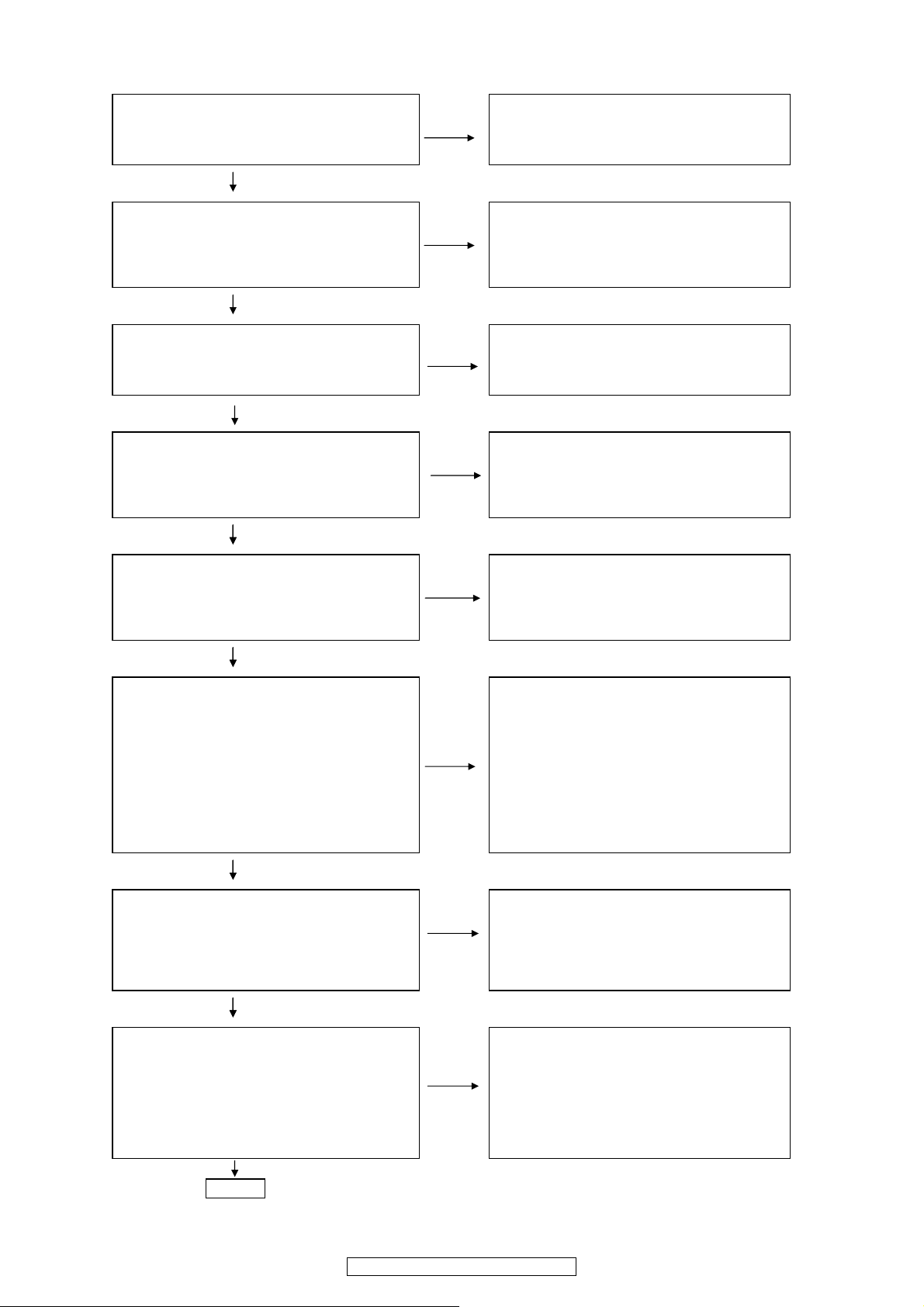
TROUBLE SHOOTING
1. FLD dosen't light
Check Fuse Check if there is any leak or short-circuiting
SMPS B'D N.G on rectifier circuit of SMPS B'D
䊶 F901 OK? Check Parts
䊶 Q903,IC93,IC92,DB91 on SMPS B'D
O.K.
Check Power Supply Voltages for System uCOM.
MAIN B'D MCU,Function Bloc䌫 N.G Check Soldering.
䊶 [BN96]:1pin ST+6V 䊶 [BN96]:1䌰䌩䌮
䊶 [D607]:Cathode 䊶 SUB TRANS B'D
䊶 [IC65]:3pin +3.3V
O.K.
Check Reset signal for System uCOM.
MAIN B'D MCU,Function Bloc䌫 N.G Check Soldering.
䊶 [IC62]:10pin RESET 䊶 IC66 on MAIN B'D
"H"level O.K.? (>2.8V)
O.K.
Check Oscillation waveform.
MAIN B'D MCU,Function Bloc䌫 N.G Check Soldering.
䊶 [IC62]:11pin 䊶 X202 on Main B'D
14.7456MHz OK?
O.K.
Check Power 50/60 Signal
MAIN B'D MCU,Function Bloc䌫 N.G Check Soldering.
䊶 [IC62]:19pin 50/60 䊶 [BN96]: 2pin
Pulse OK? 䊶 SUB TRANS B'D
O.K.
Check Power Supply Voltages for FLD Check Soldering.
FRONT B'D 䊶 FRONT B'D [BN83]:3pin +VKK
䊶 [FL81]:38pin VH (42V) 䊶 FRONT B'D [BN83]:4pin ,5pin F_AC
䊶 [FL81]:37pin VDD (3.3V) 䊶 FRONT B'D [WF81]:1pin SW+3.3V
䊶 [FL81]: 1pin F1,43pin F2 (AC3.3V) N.G 䊶 SMPS B'
D
CN93 3pin VKK
䊶 SMPS B'
D
,CN93 4pin FL+- 5pin FL-
䊶 MAIN B'
D
WN81 1pin SW+3.3V
Check Parts
䊶 SMPS B'D
Q933,Q934, IC97,D945, D935
IC94, D950 ,D933
O.K.
Check Reset Signal for FLD Check Soldering.
FRONT B'D N.G 䊶 FRONT B'D [WF81]:5pin VFD_RST1
䊶 [FL81]:35pin /RST 䊶 MAIN B'D [WN81]:5pin VFD_RST1
Hlevel O.K.? (3.3V) 䊶 [IC62]:2pin FL_RST on MAIN B'D
O.K.
Check FLD Dirive Signal for FLD Check Soldering.
FRONT B'D N.G 䊶 [WF81]: 2,3,4pin on FRONT B'D
䊶 [FL81]:32,33,34pin DA,CP,CS VFD_DI,VFD_CLK,VFD_CE
䊶 [WN81]: 2,3,4pin on MAIN B'D
VFD_DI,VFD_CLK,VFD_CE
䊶 IC62 on MAIN B'D
END
8
DRA-F107 / DRA-F107DAB
Page 9
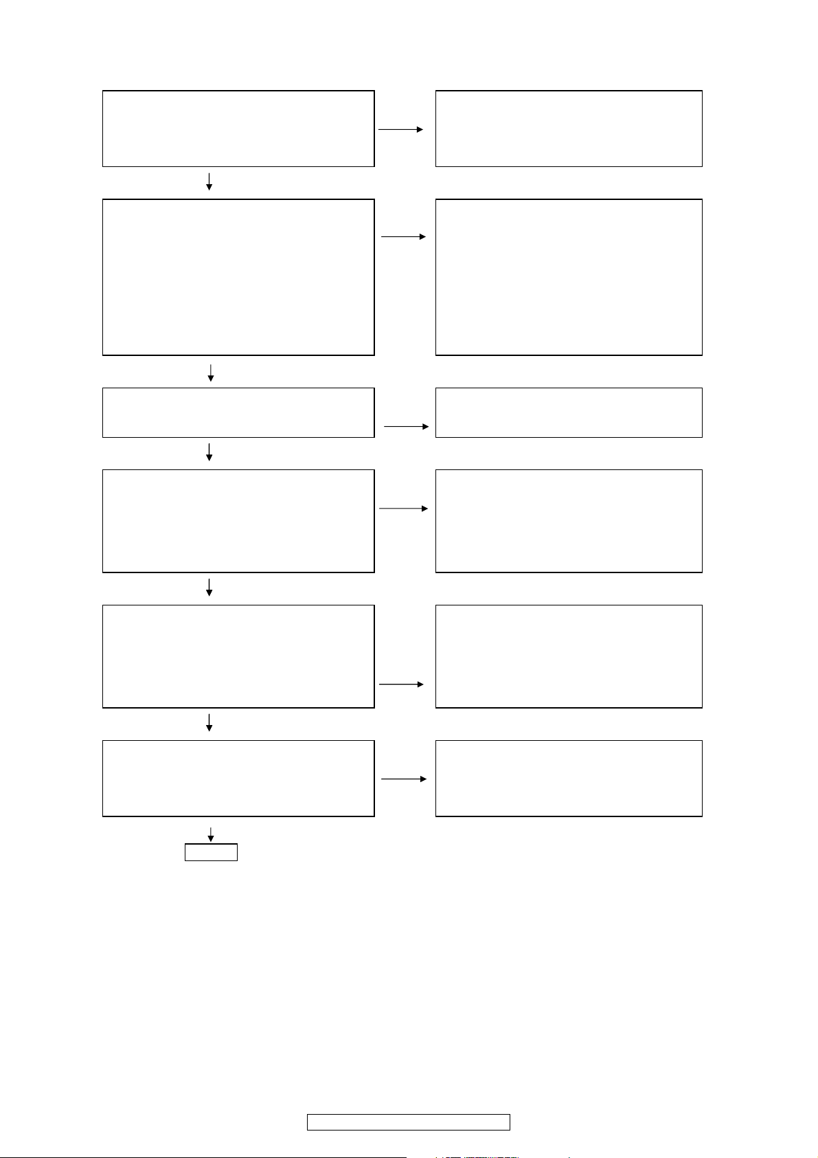
2. POWER OFF with Blinking POWER LED
Check Power Supply Voltages for Analog Block Check Soldering.
MAIN B'D MCU,Function Bloc䌫 N.G 䊶 IC22,23 on MAIN B'D
䊶䈀IC21䈁:31pin AVCC+7V 䊶䈀BN61䈁:1pin,2pin ±12V on MAIN B'D
67pin AVCC-7V 䊶䈀CN92䈁1pin,2pin ±12V on SMPS B'D
䊶 SMPS B'D IC97,IC98,D945,D931
O.K.
Check Power Supply Voltages for Digital Block Check Soldering.
MAIN B'D MCU,Function Bloc䌫 N.G MAIN B'D MCU,Function Bloc䌫
䊶䈀IC64䈁:3pin 䋫3.3V 䊶 IC64
䊶䈀WC52䈁:3pin HB+ 䊶䈀BN61䈁:4pin SW5.6V
䊶䈀WC52䈁:3pin 27VA
D.POWER AMP B'D
䈀WP52䈁:3pin 27VA
䈀CN91䈁:1,2,3,7pin 27VA
SMPS B'D
䈀BN91䈁:1,2,3,7pin 27VA
D931
O.K.
Check Protect Signal for System uCOM. Check Soldering.
MAIN B'D MCU,Function Bloc䌫 N.G MAIN B'D MCU,Function Bloc䌫
䊶 [IC62]:71pin PROT_2 High Level OK? 䊶 D371,D373,D374
O.K.
Check Protect Signal for D.Power Amp Check Soldering.
D.POWER AMP B'D N.G D.POWER AMP B'D
䊶䈀IC53䈁:3pin 12V 䊶 IC54
䊶䈀IC54䈁:17pin SD,18pin OTW,19 pin READY 䊶 IC53
High Level OK? ㇱຠ⏕
䊶 IC54,IC53
䊶 D.Power Amp Heat Sink
O.K.
Check Control Singal for DC Protect Check Soldering.
䊶 Q573_B Low Level OK? MAIN B'D MCU
䊶 Q571,572,573,574
䊶 D571,572
N.G Check Parts
䊶 Q571,572,573,574
䊶 D571,572
O.K.
Check Protect Signal for System uCOM. Check Soldering.
MAIN B'D MCU,Function Bloc䌫 N.G MAIN B'D MCU
䊶 [IC62]:74pin PROT_1 High Level OK? 䊶 D570
D.POWER AMP B'D
䊶 D504,D505,D506
END
9
DRA-F107 / DRA-F107DAB
Page 10
3. System Connector(DENON BUS) don't work
Check Power Supply Voltages for DENON BUS Check Soldering.
INPUT B'D DENON BUS BLOCK N.G INPUT B'D DENON BUS BLOCK
䊶 [WF31䈁:13pin ST5V 䊶 [WF31䈁:13pin ST5V
MAIN B'D
䊶 [WN31䈁:13pin ST5V
䊶 Q613
䊶䈀BN96䈁:1pin ST6V
䊶 D607
䊶 SUB TRANS B'D
O.K.
Check Control Signal for DENON BUS Check Soldering.
INPUT B'D DENON BUS BLOCK N.G INPUT B'D DENON BUS BLOCK
䊶 [WF31䈁:9pin BUS CLK,10pin BUS RXD_O 䊶 JK31
11pin BUS TXD_O OK? 䊶 Q301,Q302
䊶 [WF31] 9,10,11pin
MAIN B'D
[WN31] 9,10,11pin
IC31
[IC21]:26,27,28 pin
O.K.
END
4. The Key Operation don't work
Check Signal for KEY Check Soldering.
MAIN B'D N.G 䊶 WF81,S801 䌾S809,VR81,VR82 on FRONT B'D
䊶 [IC62]3,5pin F_JOG±,21,22 VJOG± 䊶 WN81,IC62 in MAIN B'D
䇭17pin PWR_KEY,93,95pin Key 0/1 OK?
O.K.
END
5. The Remote Control Operation don't work
Check Signal for Remote Control Check Soldering.
䊶䌛IC62䌝:73pin REMOTE on MAIN B'D N.G 䊶 WF81on FRONT B'D
䊶䌛RC81䌝:3pin Vcc 3.3V OK? 䊶 WN81,IC62 in MAIN B'D
O.K.
END
10
DRA-F107 / DRA-F107DAB
Page 11
6. No Sound,Noise generated
(1)CD/USB PLAY in
Check Analog Audio Data input for FUNCTION IC
MAIN B'D MCU,Function Bloc䌫 N.G Check Soldering.
䊶 [IC21] input 78,79pin 䊶 [IC21] on MAIN B'D
CD_L,CD_R 䊶 JK21
O.K.
Check Power Supply Voltages for PREAMP & POWER AMP. Check Soldering.
MAIN B'D MCU,Function Block N.G 䊶 [BN61]:1,2pin +12V,-12V,
䊶 [BN61]:1,2,4pin+12V,-12V , SW+5.6V 4pin SW+5.6V on MAIN B'D
䃨 D.POWER AMP B'D 䊶 [CN91]:1,2,3,7pin +27Von D.AMP BLOCK
䊶 [WP51]:5pin +12V 䊶䈀WP51䈁:5pin +12V
䊶 [CN91] : 1,2,3,7pin +27V 䊶 SMPS B'D IC97,IC98,D945,D931
䊶 [IC53]: 3pin +12V 䊶 SMPS B'D IC91,D951
䊶 D.POWER AMP B'D IC53
O.K.
Check Power Supply Voltages for FUNCTION IC Check Soldering.
MAIN B'D MCU,Function Bloc䌫 N.G 䊶 IC22,IC23 on MAIN B'D
䊶 [IC21]:30pin VDD (3.3V) 䊶 IC64 on MAIN B'D
31pin AVCC+7V,67pin AVCC-7V
O.K.
Check Control Signal for FUNCTION IC Check Soldering.
MAIN B'D MCU,Function Bloc䌫 N.G 䊶 IC62 on MAIN B'D
䊶 [IC21]:27,28,29pin
CLK,DATA,LATCH
O.K.
Check Analog Audio Data output from FUNCTION & Check Soldering.
PRE AMP N.G 䊶 IC21 on MAIN B'D
MAIN B'D MCU,Function Bloc䌫䊶IC24 on MAIN B'D
䊶 [IC21]:44, 39pin Lout,Rout
䊶 [IC24]:1,7 pin
O.K.
Check Audio function Mute Signal. Check Soldering.
MAIN B'D MCU,Function Bloc䌫 N.G 䊶 Q603,604, on MAIN B'D
[Q103,104]:"L"level O.K.? (-12V) 䊶 IC62 on MAIN B'D
O.K.
Check Analog Audio Data input for POWER AMP Check Soldering.
D.AMP B'D N.G 䊶 [WC51] 1,3pin on MAIN B'D,
䊶 [IC54]: 6,7pin IN_A,IN_B VOL_L_OUT,VOL_R_OUT
12,13pin IN_C, IN_D 䊶䈀WP51䈁:1,3pin on D.Power B'D
䊶 IC51,IC52 on D.AMP B'D
O.K.
Check SPEAKER RELAY control Signal Check Soldering.
MAIN B'D N.G 䊶
Q570,Q575 on MAIN B'D
䊶 [D573]:ANODE "L"level O.K.? (-12V) 䊶 [IC62] 77pin RL_MUTE on MAIN B'D
O.K.
11
DRA-F107 / DRA-F107DAB
Page 12
Check Analog Audio Data output for POWER AMP Check Soldering.
to SPEAKER. 䊶 WP52 on D.AMP BLOCK
D.POWER AMP BLOCK N.G 䊶 IC54 on D.AMP BLOCK
䊶 [IC54]:39,40pin OUT_A , 36pin OUT_B 䊶 WC52 on MAIN B'D
31pin OUT_C , 27,28pin OUT_D
MAIN B'D SP OUT BLOCK
䊶 JK51
O.K.
END
(2) AM/FM TUNER-in
Check Power Supply Voltages for AM/FM TUNER. Check Soldering.
MAIN B'D N.G 䊶 D931 on SMPS B'D
䊶 Q813, 611 on MAIN B'D
䊶䈀IC62䈁:59pin TU_PWR
O.K.
Check Control Signal for AM/FM TUNER. Check Soldering.
MAIN B'D N.G MAIN B'D
䊶 [WN21]: 7pin PLL_CE,8pin R/F_DATA 䊶 IC61,62,WN21
9pin RF_CLK,10pinPLL_DI OK?
O.K.
Check Analog Audio Data output from TUNER PACK Check Soldering.
MAIN B'D N.G 䊶 WN21 1,3 pin TU_L,TU_R on MAIN B'D
䊶 TUNER PACK output
䊶 [WN 21]:1,3pin TU_L, TU_R
䊶 [IC21]:68,69pin䇭TU_L,TU_R
O.K.
to CD/USB in 䃨Mark
(3) Portable-in(Front-in)
Check Analog Audio Data output from Prtable-in
FRONT B'D N.G Check Soldering.
䊶 Portable-in output 䊶 JK82,on FRONT B'D
䊶 BN82 1,3pin POR_L.POR_R 䊶 BN82 on FRONT B'D
O.K.
Check Analog Audio Data input for FUNCTION IC Check Soldering.
MAIN B'D MCU,Function Bloc䌫 N.G 䊶 [CN82]:1,3pin PORT_L<PORT_R on MAIN B'D
䊶 [IC21] input 2,3pin 䊶 [WP11]:10,12pin on MAIN B'D
POR_L.POR_R 䊶 [WC11]:10,12pin on MAIN B'D
䊶 [IC21]:2,3pin PORT_L,PORT_R
O.K.
to CD/USB in 䃨Mark
12
DRA-F107 / DRA-F107DAB
Page 13
(4) DAB TUNER-in
Check Power Supply Voltages for DAB TUNER UNIT. Check Soldering.
INPUT B'D DAB BLOCK N.G 䊶䈀WP82䈁:1pin DAB_PWR
䊶䈀WP82䈁:5pin 5VDD 5pin SW+5V on INPUT B'D
䊶䈀CN71䈁:2pin 3.3V 䊶 IC71,72 on INPUT B'D
䊶䈀CN71䈁:1pin 1.5V 䊶䈀WC61䈁:1pin DAB_PWR
5pin 5VDD on MAIN B'D
䊶䈀BN61䈁:5pin 5VDD on MAIN B'D
䊶 D931 on POWER B'D
䊶䈀IC62䈁:53pin DAB_PWR
Check Parts
䊶 IC71,72 on INPUT B'D
O.K.
Check Controll Signal for DAB TUNER. Check Soldering.
INPUT B'D DAB BLOCK N.G 䊶 WP82 33,34pin on DAB B'D
䊶 CN71 15,16pin DIN,DOUT 䊶 IC62
O.K.
Check Analogl Audio Data output from DAB TUNER
INPUT B'D DAB BLOCK N.G Check Soldering.
䊶 [DAB TUNER] output 䊶 [CN71]:29,30pin on DAB B'D
[CN71]: 29,30pin LOUT,ROUT
O.K.
Check Analog Audio Data input for FUNCTION IC
MAIN B'D N.G Check Soldering.
䊶 [IC21]:72,73pin DAB_L,BAD_R 䊶䈀WP82䈁:6pin,8pin on INPUT B'D
䈀WC61䈁:6pin,8pin on MAIN B'D
O.K.
to CD/USB in 䃨Mark
(5) iPod PLAY
Check Control Signal for iPod Dock Check Soldering.
MAIN B'D N.G INPUT B'D
䊶 JK32 䊶 JK32
㩷䈀WF31䈁:4,12pin IPOD_TX,IPOD_RX 䊶 [WF31]: 4,12pin IPOD_TX,IPOD_RX
㪤㪘㪠㪥㩷㪙㩾㪛
䊶 [WN31]: 4,12pin IPOD_TX,IPOD_RX
䊶 [ IC62]:29,30pin
䊶 IC61
O.K.
Check Analog signal output from iPod Dock Check Soldering.
MAIN B'D N.G 䊶 JK21 on MAIN B'D
䊶 JK21 AUXi in L,R
䊶 [IC21]:71,71pin AUX1_L,AUX1_R
O.K.
to CD/USB in 䃨Mark
13
DRA-F107 / DRA-F107DAB
Page 14
(6) PHONO PLA
Y
Check Power Supply Voltages for PHONO Check Soldering.
INPUT B'D PHONO BLOCK N.G 䊶䈀WP11䈁:4pin-7V,5pin +7V
䊶䈀WP11䈁:4pin-7V,5pin +7V 䊶䈀WC11䈁:4pin-7V,5pin +7V on Main B'D
O.K.
Check Soldering.
Check Analog signal input for FUNCTION IC 䊶 [IC21]:80,1pin PHONO_L,PHONO_R
MAIN B'D N.G 䊶
䈀
㪮㪚㪈㪈䈁㪑㪈㪃㪊㫇㫀㫅
䊶 [IC21]:49,50pin LOUT,ROUT 䊶
䈀
㪮㪧㪈㪈䈁㪑㪈㪃㪊㫇㫀㫅
䊶 IC11
䊶 JK11
O.K.
to CD/USB in 䃨Mark
(7) Head Phone OUT
Check Analog signal output forom FUNCTION IC Check Soldering.
MAIN B'D N.G MAIN B'D
䊶 [IC21]:54pin LOUT,47pin ROUT 䊶 [IC21]:54pin LOUT,47pin ROUT
㪫㪦㩷㩿㪈㪀㪚㪛ౣ
↢
O.K.
Check Power Supply Voltages for Head Phone Amp Check Soldering.
INPUT B'D H/P AMP BLOCK N.G 䊶 䈀㪮㪧㪈㪈䈁㪑㪋㫇㫀㫅㩷㪄㪎㪭㪃㩷㪌㫇㫀㫅㩷㪂㪎㪭㩷㫆㫅㩷㪠㪥㪧㪬㪫㩷㪙㩾㪛
䊶 䈀㪮㪧㪈㪈䈁㪑㪋㫇㫀㫅㩷㪄㪎㪭㪃㩷㪌㫇㫀㫅㩷㪂㪎㪭 䊶 䈀㪮㪚㪈㪈䈁㪑㪋㫇㫀㫅㩷㪄㪎㪭㪃㩷㪌㫇㫀㫅㩷㪂㪎㪭㩷㫆㫅㩷㪤㪘㪠㪥㩷㪙㩾㪛
O.K.
Check Soldering.
Check Mute Control signal for Head Phone INPUT B'D H/P BLOCK
INPUT B'D H/P BLOCK N.G 䊶
䈀
WP11䈁:13pin HP_MUTE
䊶
䈀
WP11䈁:13pin HP_MUTE Low Level OK?(-7V) MAIN B'D
䈀
WC11䈁:13pin HP_MUTE
O.K.
Check Soldering.
Check Analog signal output from Head Phone Amp 䊶
䈀
㪮㪚㪈㪈䈁㪎㫇㫀㫅㩷㪟㪧㪶㪣㪠㪥㪃㪏㫇㫀㫅㩷㪟㪧㪶㪩㪠㪥㩷㫆㫅㩷㪤㪘㪠㪥㩷㪙㩾㪛
INPUT B'D H/P BLOCK N.G INPUT B'D H/P BLOCK
䊶 [IC13]:1pin LOUT,7pin ROUT 䊶
䈀
㪮㪧㪈㪈䈁㪎㫇㫀㫅㩷㪟㪧㪶㪣㪠㪥㪃㪏㫇㫀㫅㩷㪟㪧㪶㪩㪠㪥㩷㫆㫅㩷㪤㪘㪠㪥㩷㪙㩾㪛
㪝㫉㫆㫅㫋㩷㪙㩾㪛 䊶 IC13
䊶
䈀
㪙㪥㪏㪉䈁㪑㪌㫇㫀㫅㩷㪟㪧㪶㪣㪦㪃㪍㫇㫀㫅㩷㪟㪧㪶㪩㪦 䊶䈀㪚㪥㪏㪉䈁㪑㪌㫇㫀㫅㩷㪟㪧㪶㪣㪦㪃㪍㫇㫀㫅㩷㪟㪧㪶㪩㪦
㪝㫉㫆㫅㫋㩷㪙㩾㪛
䊶
䈀
㪙㪥㪏㪉䈁㪑㪌㫇㫀㫅㩷㪟㪧㪶㪣㪦㪃㪍㫇㫀㫅㩷㪟㪧㪶㪩㪦
㪚㪿㪼㪺㫂㩷㪧㪸㫉㫋㫊
Q105,Q106,Q107,Q108
O.K.
END
14
DRA-F107 / DRA-F107DAB
Page 15
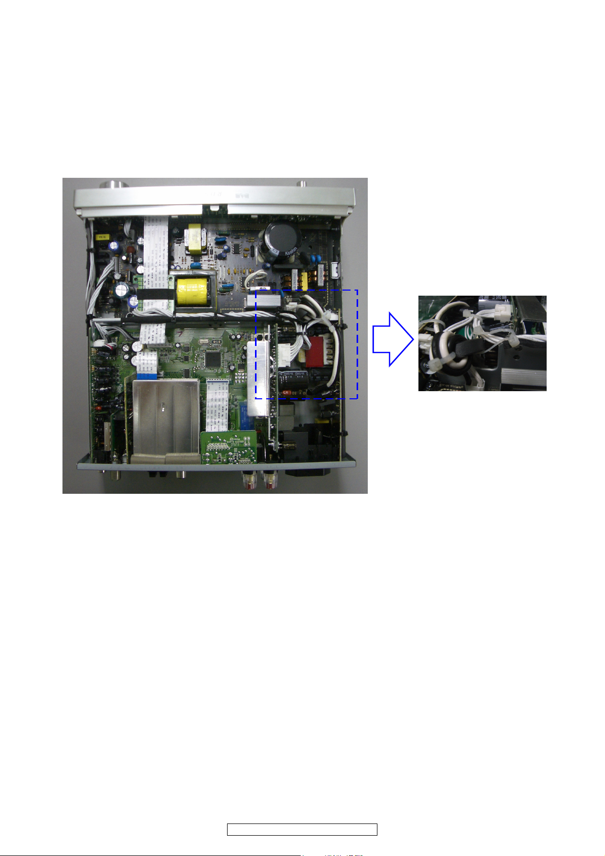
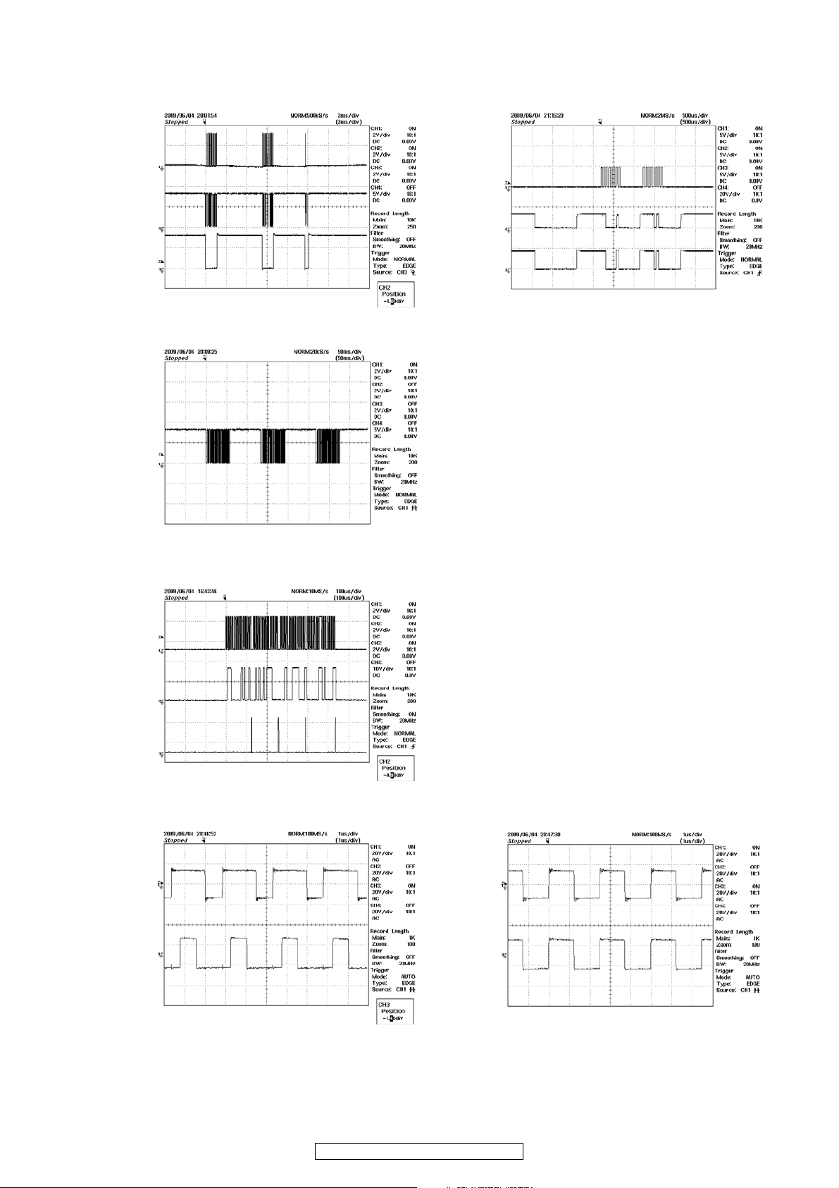
MEASURING POINT AND WAVEFORMS
Detail A
e
w
A
q
㩷
r
y
t
W2
W1
MEASURING POINT
FRONT PCB
UPDATE PCB
15
DRA-F107 / DRA-F107DAB
Page 16
MAIN PCB
㪛㪼㫋㪸㫀㫃㩷㪚
㪛㪼㫋㪸㫀㫃㩷㪛
㪛㪼㫋㪸㫀㫃㩷㪙
Q7
o
㪙
㪚
㪛
,
Q3 Q4
Q0
Q1
u
Q5
Q6
Q8
16
DRA-F107 / DRA-F107DAB
Page 17
POWER AMP
Q2
Q1
Q9
W0
DAB PCB
17
DRA-F107 / DRA-F107DAB
Page 18
WAVEFORMS
FLD Drive Signal DENON BUS
䊶Mode:Fanction Selec
t
䊶Mode:Push Remote Control "CD Pla
y"
qFL_D
A
rBUS_CL
K
wFL_CP
tBUS
RXD
eFL
CS
yBUS
TXD
Remote Control
䊶Mode:Push Remote Control "SOURCE"
uREMOTE
CD/USB INPUT
䊶Mode:Fanction Selec
t
iCL
K
oDAT
A
Q0LATCH
CD/USB Play
䊶Mode: CD INPUT=200mVrms,1kHz S
p
eaker=4ohm 䊶Mode: CD INPUT=Open䇮Speaker=4ohm
Q1OUTA Q1OUTA
Q2OUTB Q2OUTB
_
_
_
18
DRA-F107 / DRA-F107DAB
Page 19
䊶Mode: CD INPUT=200mVrms,1kHz Speaker=4ohm 䊶Mode: CD INPUT=Open䇮Speaker=4ohm
Q1OUTA Q1OUTA
Q3SPEAKE
R
Q3SPEAKE
R
OUT FL+ OUT FL+
Q4SPEAKE
R
Q4SPEAKE
R
OUT FL- OUT FL-
AM/FM TUNER INPUT
䊶Mode:Function CD㸢Tuner FM 䊶Mode:Tuner Band FM㸢
A
M
Q5PLL
CE Q5PLL_CE
Q6R/F
DAT
A
Q6R/F_DAT
A
Q7R/F_CL
K
Q7R/F_CL
K
Q8PLL_DI Q8PLL_DI
DAB TUNER INPUT iPod Play
䊶Mode:Tuner Band AM㸢DAB 䊶Mode:iPod Connec
t
W1IPOD_TX
Q9DIN
W2IPOD
RX
W0DOUT
_
_
_
19
DRA-F107 / DRA-F107DAB
Page 20
SEMICONDUCTORS
75
76
1
100
51
50
26
25
Only major semiconductors are shown, general semiconductors etc. are omitted to list.
The semiconductor which described a detailed drawing in a schematic diagram are omitted to list.
1. IC’s
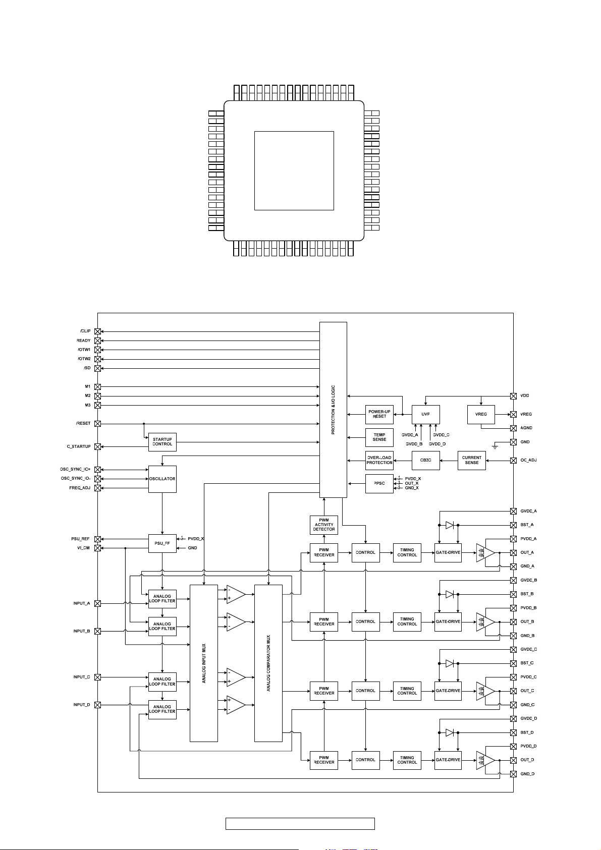
M3062LFGPGP (IC62)
M3062LFGPGP Terminal Function
Pin
No.
1 P94 O [LED_RL] [STANDBY Red LED output. ON:High] L
2 P93 O FL RESET Reset output to FLD L
3 TB2IN I FUNC_JOGB FUNCTION encoder Pulse-B input HI-Z
4 P91 O Not Used:N.C. L
5 TB0IN I FUNC_JOGA FUNCTION encoder Pulse-A input HI-Z
6 BYTE (VSS) GND -
7 CNVSS I FLASH CNVss Select input of Flash rom write mode HI-Z
8 P87 O Not Used:N.C. L
9 P86 O Not Used:N.C. L
10 RESET I RESET Reset input HI-Z
11 XOUT XTAL(16MHz) Xtal output -
12 VSS (VSS) GND -
13 XIN XTAL(16MHz) Xtal input -
14 VCC (VCC) Positive power -
15 NMI I (PullUp) Pull up HI-Z
16 P84 O Not Used:N.C. L
17 INT1 INT POWER KEY Power button input (interrupt input) HI-Z
18 INT0 INT /DBRXD DENON BUS Data input (interrupt input) HI-Z
19 P81 I 50/60 50Hz/60Hz AC Input HI-Z
20 P80 I H/P SW HEAD PHONE insert detect signal input HI-Z
21 TA3IN I VOL JOGB VOL encoder Pulse-B input HI-Z
22 TA3OUT I VOL JOGA VOL encoder Pulse-A input HI-Z
23 P75 O FLCS Chip Select output to FLD L
24 P74 O LED G POWER/SANDBY Green LED output. ON:High L
25 P73 O LED R POWER/SANDBY Red LED output. ON:High L
26 CLK2 O /DBCLK(DENON BUS) Serial Clock output for DENON BUS H
27 RXD2 I /DBRXD(DENON BUS) Serial Data input for DENON BUS HI-Z
Port
Function
Port
setting
Port Name Explaanation
Output of
Standby &
Default
20
DRA-F107 / DRA-F107DAB
Page 21
Pin
No.
28 TXD2 O /DBTXD(DENON BUS) Serial Data output for DENON BUS H
29 TXD3 SO IPOD_TX Serial Data output for IPOD DOCK L
30 RXD3 SI IPOD_RX Serial Data input for IPOD DOCK HI-Z
31 CLK1 I (PULLDOWN) Pull down L
32 P64 O Not Used:N.C. L
33 P63 SO S1_DIN Serial Data output to DAB Module L
34 P62 SI SI_DOUT Serial Data input from DAB Module L
35 P61 O Not Used:N.C. L
36 P60 O Not Used:N.C. L
37 P57 O.D Not Used:N.C. L
38 P56 O Not Used:N.C. L
39 P55 I (FLASH EPM) Not Used:N.C. HI-Z
40 P54 SO E2P CLK Serial Clock output to EEPROM L
41 P53 SI E2P DO Serial Data input from EEPROM HI-Z
42 P52 SO E2P DI Serial Data output to EEPROM L
43 P51 O E2P CS Chip Enable output to EEPROM L
44 P50 O (FLASH CE) Not Used:N.C. H
45 P47 O Not Used:N.C. L
46 P46 I PWB check Pull down HI-Z
47 P45 I PWB check Pull down HI-Z
48 P44 I PWB check Pull down HI-Z
49 P43 I PWB check Pull down HI-Z
50 P42 O Not Used:N.C. L
51 P41 O Not Used:N.C. L
52 P40 O Not Used:N.C. L
53 P37 O /FMAM TUNER Select to DAB or AM/FM . DAB:High AM/FM:Low L
54 P36 O TU/PHO
55 P35 O Not Used:N.C. L
56 P34 O Not Used:N.C. L
57 P33 O SW MUTE MUTE output for SW OUTPUT H
58 P32 O Not Used:N.C. L
59 P31 O TP.ON/OFF (TPOWER) AM/FM TUNER Power ON/OFF Switching output L
60 (VCC) Positive power -
61 P30 O Not Used:N.C. L
62 (VSS) GND -
63 P27 O Not Used:N.C. L
64 P26 I STEREO "STEREO" indicator input from FM/AM TUNER pack HI-Z
65 P25 I TUNED "TUNED" detect input from FM/AM TUNER pack HI-Z
66 P24 O T.MUTE MUTE output for FM/AM TUNER pack L
67 P23 O SANYO CE Chip Enable output to PLL/RDS IC L
68 P22 O SANYO DI Serial Data input to PLL/RDS IC L
69 P21 O SANYO CLK Serial Clock output to PLL/RDS IC L
70 P20 I SANYO DO Serial Data output to PLL/RDS IC HI-Z
71 P17 I PROTECT2 Protect Signal input 2 HI-Z
72 P16 O /SYR Reset output to RDS IC L
73 INT3 INT REMOTE Remote Control signal input HI-Z
74 P14 I PROTECT1/SP
75 P13 O /BUF_EN Enable signal output fot BUS BUFFER IC H
76 P12 O VR MUTE MUTE output for POWER AMP H
77 P11 O RL(RMUTE) SPEAKER RELAY ON/OFF output L
78 P10 O AP.ON/OFF (APOWER)
79 P07 O H/P MUTE MUTE output for HEAD PHONE output L
80 P06 O P.ON/OFF (POWER) MAIN POWER ON/STANDBY Switching output ON:High L
81 P05 O Not Used:N.C. L
Port
Function
Port
setting
Port Name Explaanation
REC.OUTPUT level Select to TU/PHO or Others . TU/PHO:High
Protect Signal input 1 HI-Z
PROTECTION
± 15V POWER ON/OFF Switching output ON:Hight
Output of
Standby &
Default
L
L
21
DRA-F107 / DRA-F107DAB
Page 22

Pin
No.
82 P04 O [RECOUT MUTE] [MUTE output for REC.OUTPUT] L
83 P03 O M61531_DATA Serial Data output to M61531 L
84 P02 O M61531_CLK Serial Clock output to M61531 L
85 P01 O M61531_LATCH Latch output to M61531 L
86 P00 I PORT.IN_SW PORTABL INPUT insert detect signal input HI-Z
87 P107 I Pull up HI-Z
88 P106 I USA Initial Setting input HI-Z
89 P105 I EURO Initial Setting input HI-Z
90 P104 I Pull up L
91 AN3 AD FREQ Initial Setting input HI-Z
92 AN2 AD RDS Initial Setting input HI-Z
93 AN1 AD KEY 0 Unit Operation Button input 0 HI-Z
94 (VSS) GND -
95 AN0 AD KEY 1 Unit Operation Button input 1 HI-Z
96 VREF (VCC) Positive power -
97 AVCC (VCC) Positive power -
98 P96 O Not Used:N.C. L
99 P97 SO FLDA Serial Data output to FLD L
100 P95 SO FLCK Serial Clock output to FLD L
Port
Function
Port
setting
Port Name Explaanation
Output of
Standby &
Default
22
DRA-F107 / DRA-F107DAB
Page 23
M61531FP (IC21)
Block Diagram and Pin Configuration (Top View)
CIN2
80
79
78
77
76
75
74
73
72
71
70
69
68
67
66
65
1
2
3
4
5
6
7
8
9
10
11
64
63
62
61
60
59
58
57
56
55
54
25
26
27
28
29
30
31
32
33
34
35
36
37
38
39
40
11
12
13
14
15
16
17
18
19
20
21
22
23
GND
INL3
INL10/RECL4
SWIN2
SLVIN
SLSELOUT
CSELOUT
CVIN
COUT
SWOUT
SWVIN
SWSELOUT
GND
AVCC
DVDD
LATCH
DATA
CLOCK
DGND
INR10/RECR4
AVEE
INL9
INR9
INL8
INR8
INL7
INR7
INL6
INR6
INL5
INR5
INL4
INR4
SLOUT
SROUT
SRVIN
SRSELOUT
RSELOUT
RVIN
ROUT
TRE R
BASS R2
BASS R1
BASS L1
BASS L2
TRE L
LOUT
LVIN
LSELOUT
GND
RECL1
RECR1
RECL2
RECR2
RECL3
RECR3
INR3
INR2
INL2
INL1/EXT INL
INR1/EXT INR
GND
CIN1
SWIN1
SRIN1
SLIN1
LIN1
RIN1
BALANCE L/+
BALANCE R/+
LOUD R
/BALANCE R/−
LOUD L
/BALANCE L/−
GND
GND
GND
LIN2
RIN2
SRIN2
SLIN2
24
53
52
51
50
49
48
47
46
45
44
43
42
41
Input
Gain
Control
Input
Gain
Control
Input
Gain
Control
Input
Gain
Control
Input
Gain
Control
Input
Gain
Control
Output
Gain
Control
Rch
Lch
SLch
SRch
SWch
Cch
Output
Gain
Control
Output
Gain
Control
Output
Gain
Control
Output
Gain
Control
MCU I/F
CLK
DATA
LATCH
Lch VOL
Output
Gain
Control
Rch VOL
SRch VOL
SLch VOL
Cch
VOL
SWch
VOL
Input ATT
Input ATT
Lch
Rch
GND
GND
DVDDAVCC
AVEE
SWch
Cch
SLch
SRch
Rch
Lch
Rch
Lch
Rch
GND
GND
Lch
GND
GND
L/R VOL
Input
L/R VOL
Input
Multi
Input Selector
Multi
Input Select or
Multi
Input Selector
Multi
Input Selector
GND
Tone(Bass,Treble)
Lch
Rch
R1
L1
R1
L1
-1
-1
R2
L2
R2
L2
Loudness tap
Loudness tap
Loudness tap
Loudness tap
Bypass/Tone
Bypass/Tone
Bypass/Tone
Bypass/Tone
Tone Block Position
Tone Block Position
Loud
/Balance
Loud
/Balance
R3
L3
L3
R3
Tone
Input
ATT
Tone
Input
ATT
Bypass
Selector
23
DRA-F107 / DRA-F107DAB
Page 24

Pin Description
Pin No. Pin Name Function
3, 1, 79, 77, 75, 73, 71, 69 INR2, 3, 4, 5, 6, 7, 8, 9 Input pin of R channel (Input Selector)
2, 80, 78, 76, 74, 72, 70, 68 INL2, 3, 4, 5, 6, 7, 8, 9 Input pin of L channel (Input Selector)
4 INL1/EXT INL
Input pin of L channel (Input Selector)/External Input pin(Lch)
5 INR1/EXT INR
Input pin of L channel (Input Selector)/External Input pin(Rch)
6, 13, 16, 19, 32, 57, 64 GND Analog Ground
7, 24 CIN1/CIN2 Input pin of C channel (2 Input Selector)
8, 25 SWIN1/SWIN2 Input pin of SW channel (2 Input Selector)
9, 22 SRIN1/SRIN2 Input pin of SR channel (2 Input Selector)
10, 23 SLIN1/SLIN2 Input pin of SL channel (2 Input Selector)
11, 20 LIN1/LIN2 Input pin of L channel (2 Input Selector)
12, 21 RIN1/RIN2 Input pin of R channel (2 Input Selector)
14, 17 BALANCE L/+, R/+ Output pin of L/R channel Balance Output(+)
15, 18 LOUD L/BALANCE L/–,
LOUD R/BALANCE R/–
Frequency characteristic setting pin of Loudness
/Output pin of L/R channel Balance Output(–)
26 DGND Ground of internal logic circuit
27, 28, 29 CLOCK, DATA, LATCH Input pin of control clock /data/ trigger
30 DVDD Power supply to internal logic circuit
31 AVCC Positive power supply to internal analog circuit
33 SWSELOUT Output pin of SW channel volume input selector
34 SWVIN Input pin of SW channel volume
35 SWOUT Output pin of SW channel
36 COUT Output pin of C channel
37 CVIN Input pin of C channel volume
38 CSELOUT Output pin of C channel volume input selector
39 SLSELOUT Output pin of SL channel volume input selector
40 SLVIN Input pin of SL channel volume
41 SLOUT Output pin of SL channel
42 SROUT Output pin of SR channel
43 SRVIN Input pin of SR channel volume
44 SRSELOUT Output pin of SR channel volume input selector
45 RSELOUT Output pin of R channel volume input selector
46 RVIN Input pin of R channel volume
47 ROUT Output pin of R channel
51, 52, 50, 49 BASS L1, L2/BASS R1, R2
Frequency characteristic setting pin of tone control (BASS)
53, 48 TRE L/TRE R
Frequency characteristic setting pin of tone control (TREBLE)
54 LOUT Output pin of L channel
55 LVIN Input pin of L channel volume
56 LSELOUT Output pin of L channel volume input selector
58, 60, 62/59, 61, 63 REC L1, L2, L3
/REC R1, R2, R3
Output pin of REC (Lch and Rch)
65 INL10/REC L4
Input pin of L channel (Input Selector)/Output pin of REC (Lch)
66 INR10/REC R4
Input pin of R channel (Input Selector)/Output pin of REC (Rch)
67 AVEE Negative power supply to internal analog circuit
DRA-F107 / DRA-F107DAB
24
Page 25
TAS5630DKD (IC54)
26
16
15
OC_ADJ
14
/RESET
13
C_STARTUP
12
INPUT_A
11
INPUT_B
10
VI_CM
9
GND
8
AGND
7
VREG
6
INPUT_C
5
INPUT_D
4
FREQ_ADJ
3
OSC_IO+
2
OSC_IO-
1
/SD
64-pins QFP package
32
GND_D
31
PVDD_D
30
PVDD_D
29
OUT_D
28
OUT_D
27
BST_D
GVDD_D
25
GVDD_C
24
GND
23
GND
22NC21
NC
20NC19
NC
18
PSU_REF
17
VDD
33
GND_D
34
GND_C
35
GND_C
36
OUT_C
37
OUT_C
38
PVDD_C
39
PVDD_C
40
BST_C
41
BST_B
42
PVDD_B
43
OUT_B
44
GND_B
45
GND_A
46
47
48
55
49
/OTW2
50
/CLIP
51
READY
52M153M254
M3
GND
56
GND
57
GVDD_B58GVDD_A
59
BST_A
60
OUT_A
61
OUT_A
62
PVDD_A
63
PVDD_A
64
GND_A
/OTW1
PVDD_B
OUT_B
GND_B
TAS5630DKD Block Diagram
25
DRA-F107 / DRA-F107DAB
Page 26

TAS5630DKD Terminal Function
TERMINAL
NAME PHD NO.
DKD NO.
FUNCTION
(1)
DESCRIPTION
AGND 8 10
P Analog ground
BST_A 54 43
P HS bootstrap supply (BST), external 0.033 uF capacitor to OUT_A required.
BST_B 41 34
P HS bootstrap supply (BST), external 0.033 uF capacitor to OUT_B required.
BST_C 40 33
P HS bootstrap supply (BST), external 0.033 uF capacitor to OUT_C required.
BST_D 27 24
P HS bootstrap supply (BST), external 0.033 uF capacitor to OUT_D required.
/CLIP 18 -
O Clipping warning; open drain; active low
C_STARTUP 3 5
O Startup ramp requires a charging capacitor of 4.7 nF to AGND in BTL mode.
FREQ_ADJ 12 14
I PWM frame rate programming pin requires resistor to AGND
GND 7,23,24,57,58 9
P Ground
GND_A 48, 49 38
P Power ground for half-bridge A
GND_B 46, 47 37
P Power ground for half-bridge B
GND_C 34, 35 30
P Power ground for half-bridge C
GND_D 32, 33 29
P Power ground for half-bridge D
GVDD_A 55 -
P Gate drive voltage supply requires 0.1 uF capacitor to GND_A
GVDD_B 56 -
P Gate drive voltage supply requires 0.1 uF capacitor to GND_B
GVDD_C 25 -
P Gate drive voltage supply requires 0.1 uF capacitor to GND_C
GVDD_D 26 -
P Gate drive voltage supply requires 0.1 uF capacitor to GND_D
GVDD_AB - 44
P Gate drive voltage supply requires 0.22 uF capacitor to GND_A/GND_B
GVDD_CD - 23
P Gate drive voltage supply requires 0.22 uF capacitor to GND_C/GND_D
INPUT_A 4 6
I Input signal for half bridge A
INPUT_B 5 7
I Input signal for half bridge B
INPUT_C 10 12
I Input signal for half bridge C
INPUT_D 11 13
I Input signal for half bridge D
M1 20 20
I Mode selection
M2 21 21
I Mode selection
M3 22 22
I Mode selection
NC 59-62 -
- No connect, pins may be grounded.
OC_ADJ 1 3
O Analog over current programming pin requires resistor to ground.
OSC_IO+ 13 15
I/O Oscillaotor master/slave output/input.
OSC_IO- 14 16
I/O Oscillaotor master/slave output/input.
/OTW - 18
O Overtemperature warning signal, open drain, active low.
/OTW1 16 -
O Overtemperature warning signal, open drain, active low.
/OTW2 17 -
O Overtemperature warning signal, open drain, active low.
OUT_A 52, 53 39, 40
O Output, half bridge A
OUT_B 44, 45 36
O Output, half bridge B
OUT_C 36, 37 31
O Output, half bridge C
OUT_D 28, 29 27, 28
O Output, half bridge D
PSU_REF 63 1
P PSU Reference requires close decoupling of 330 pF to AGND
PVDD_A 50, 51 41, 42
P
Power supply input for half bridges A requires close decoupling of 2.2-uF capacitor
to GND_A
PVDD_B 42, 43 35
P
Power supply input for half bridges B requires close decoupling of 2.2-uF capacitor
to GND_B
PVDD_C 38, 39 32
P
Power supply input for half bridges C requires close decoupling of 2.2-uF capacitor
to GND_C
PVDD_D 30, 31 25, 26
P
Power supply input for half bridges D requires close decoupling of 2.2-uF capacitor
to GND_D
READY 19 19
O Normal operation; open drain; active high
/RESET 2 4
I Device reset Input; active low, requires 47kOhm pull up resistor to VREG.
/SD 15 17
O Shutdown signal, open drain, active low
VDD 64 2
P
Power supply for internal voltage regulator requires a 10-uF capacitor in parallel
with a 0.1-uF capacitor to GND for decoupling.
VI_CM 6 8
O
Analog comparator reference node requires close decoupling of
1 nF to AGND
VREG 9 11
P Internal regulator supply filter pin requires 0.1-uF capacitor to AGND
(1) I = input, O = output, P = power
26
DRA-F107 / DRA-F107DAB
Page 27

ICE2QS01 (IC93)
Pin Symbol Function
1 ZC Zero Crossing
2 REG Regulation
3 CS Primary Current Sensing
4, 5 HV High Voltage input
6 OUT gate driver out put
7 VCC IC supply voltage
8 GND Common ground
1
6
7
8
4
3
2
5
GNDZC
REG
CS
VCC
OUT
HV
HV
Blockdigram
GND
8
CS
3
REG
2
OUT
6
ZC
1
controller
V
os
OLP
VCC
OVP
VCC
UVP
output
OVP
current limitation /
foldback correction
V
V
V
V
auto
restart
latch
off
current measurement
V
SWP
V
REF
R
ZCT2
VCCOVP
vccuvp
OPOVP
csSW
v1
power management
Reg
Vcsth
on/off FF
gate driver
PWM generator
Zero-crossing
counter
up/down
counter
HV
4, 5
VCC
7
power cell
V
OLP
active burst
control
ringing
suppression
time control
V
ZCT1
27
DRA-F107 / DRA-F107DAB
Page 28

ICE2QS01 Functional description
Functional Description
3 Functional Description
3.1 VCC Pre-Charging and Typical
VCC Voltage During Start-up
In the controller ICE2QS01, a power cell is integrated.
As shown in Figure 2, the power cell consists of a high
voltage device and a controller, whereby the high
voltage device is controlled by the controller. The
power cell provides a pre-charging of the VCC
capacitor till VCC voltage reaches the VCC turned-on
threshold V
VCCon
and the IC begins to operate, while it
may keep the VCC voltage at a constant value during
burst mode operation when the output voltage is pulled
down or the power from the auxiliary winding is not
enough, or when the IC is latched off in certain
protection mode.
Once the mains input voltage is applied, a rectified
voltage shows across the capacitor C
bus
. The high
voltage device provides a current to charge the VCC
capacitor C
vcc
. Before the VCC voltage reaches a
certain value, the amplitude of the current through the
high voltage device is only determined by its channel
resistance and can be as high as several mA. After the
VCC voltage is high enough, the controller controls the
high voltage device so that a constant current around
1mA is provided to charge the VCC capacitor further,
until the VCC voltage exceeds the turned-on threshold
V
VCCon
. As shown as the time phase I in Figure 3, the
VCC voltage increase near linearly.
Figure 3 VCC voltage at start up
The time taking for the VCC pre-charging can then be
approximately calculated as:
[1]
where I
VCCcharge2
is the charging current from the power
cell which is 1.05mA, typically.
Exceeds the VCC voltage the turned-on threshold
V
VCCon
of at time t1, the power cell is switched off, and
the IC begins to operate with a soft-start. Due to power
consumption of the IC and the fact that still no energy
from the auxiliary winding to charge the VCC capacitor
before the output voltage is built up, the VCC voltage
drops (Phase II). Once the output voltage is high
enough, the VCC capacitor receives then energy from
the auxiliary winding from the time point t
2
on. The VCC
then will reach a constant value depending on output
load.
Since there is a VCC undervoltage protection, the
capacitance of the VCC capacitor should be selected to
be high enough to ensure that enough energy is stored
in the VCC capacitor so that the VCC voltage will never
touch the VCC under voltage protection threshold
V
VCCUVP
before the output voltage is built up. Therefore,
the capacitance should fulfill the following requirement:
[2]
with I
VCCop
the operating current of the controller.
3.2 Soft-start
At the time t1, the IC begins to operate with a soft-start.
By this soft-start the switching stresses for the switch,
diode and transformer are minimised. The soft-start
implemented in the ICE2QS01 is a digital time-based
function. The preset soft-start time is 24ms with 8
steps. The internal reference for the regulation voltage
begins at 1.35V and with an increment of 0.35V for
each following step.
3.3 Normal Operation
The PWM section of the IC can be divided into two
main portions: PWM controller for normal operation
and PWM controller for burst mode operation. The
PWM controller for normal operation will be described
in the following paragraphs, while the PWM controller
for burst mode operation will be discussed in the next
section.
The PWM controller for normal operation consists of
digital signal processing circuit including an up/down
counter, a zero-crossing counter (ZC-counter) and a
comparator, and analog circuit including a current
measurement unit and a comparator. The switch-on
and -off time point is determined by the digital circuit
and the analog circuit, respectively. As input
information for the switch-on determination, the zerocrossing input signal and the value of the up/down
counter are needed, while the feedback signal v
REG
and the current sensing signal vCS are necessary for
the switch-off determination. Details about the
operation of the PWM controller in normal operation
are illustrated in the following paragraphs.
3.3.1 Switch-on Determination
As mentioned above, the digital signal processing
circuit consists of an up/down counter, a zero-crossing
counter and a comparator. A ringing suppression time
V
VCCon
VCC
V
VCCUVP
t1
t
t2
iiiiii
t
1
V
VCConCvcc
I
VCCch e2arg
--------------------------------- -=
C
vcc
I
VCCopt2t1
–
V
VCConVVCCUVP
–
------------------------------------------------t
DRA-F107 / DRA-F107DAB
28
Page 29

Functional Description
controller is implemented to avoid mistriggering by the
ring after MOSFET is turned off. Functionality of these
parts is described as in the following.
3.3.1.1 Up/down Counter
The up/down counter stores the number of zero
crossing to be ignored before the main power switch is
switched on after demagnetisation of the transformer.
This value is a function of the regulation voltage, which
contains information about the output power.
Generally, a high output power results in a high
regulation voltage. According to this information, the
value in the up/down counter is changed to a low value
in case of high regulation voltage, and to a high value
in case of low regulation voltage. In ICE2QS01, the
lowest value of the counter is 1 and the highest 7.
Following text explains how the up/down counter value
changes in responding to the regulation voltage v
REG
.
The regulation voltage v
REG
is internally compared with
three thresholds V
RL
, VRH and VRM. According to the
results, the value in the up/down counter is changed,
which is summarised in Table 1 and Figure 4
respectively.
Table 1 Operation of the up/down counter
Figure 4 Up/down counter operation
According to the comparison results the up/down
counter counts upwards, keeps unchanged or counts
downwards. However, the value in up/down counter is
limited between 1 and 7. If the counter tends to count
beyond this range, the attempt is ignored.
In normal case, the up/down counter can only be
changed by one each time at the clock period of 48ms.
However, to ensure a fast response to sudden load
increase, the counter is set to 1 in the following
switching period after the regulation voltage v
REG
exceeds the threshold VRM.
3.3.1.2 Zero-Crossing Counter and Ringing
Suppression Time Controller
In the system, the voltage from the auxiliary winding is
applied to the zero-crossing pin through a RC network,
which provides a time delay to the voltage from the
auxiliary winding. Internally, this pin is connected to a
clamping network, a zero-crossing detector, an output
overvoltage (OP OVP) detector and a ringing
suppression time controller.
During on-state of the power switch a negative voltage
applies to the ZC pin. Through the internal clamping
network, the voltage at the pin is clamped to certain
level. However, it is highly recommended that a fastrecovery diode D
zc
is added to block the negative
voltage when the power switch is on. This is because
the device in MOS technology is sensitive to negative
voltage.
The voltage at the ZC pin v
ZC
is compared with the
threshold V
ZCT1
. Once the voltage vZC crosses the
threshold at its falling edge, a pulse is generated which
is fed to the zero-crossing counter and the counter
value increases by 1.
After MOSFET is turned on, there will be some
oscillation on V
DS
, which will also appear on the voltage
on ZC pin. To avoid the MOSFET is turned on
mistriggerred by such oscillation, a ringing suppression
timer is implemented. The time is dependent on the
voltage v
ZC
. When the voltage v
ZC
is lower than the
threshold V
ZCT2
, a longer preset time applies, while a
shorter time is set when the voltage v
ZC
is higher than
the threshold.
The voltage v
ZC
is used for the output overvoltage
protection, as well. Once the voltage at this pin is
higher than the threshold V
OPOVP
during off-time of the
main switch, the IC is latched off after a fixed blanking
time.
To achieve the switch-on at voltage valley, the voltage
from the auxiliary winding is fed to a time delay network
(the RC network consists of D
zc
, R
zc1
, R
zc2
and Czcas
shown in typical application circuit) before it is applied
to the zero-crossing detector through the ZC pin. The
needed time delay to the main oscillation signal 't
should be approximately one fourth of the oscillation
period (by transformer primary inductor and drainsource capacitor) minus the propagation delay from the
v
REG
up/down counter
action
Always lower than V
RL
Count upwards till
7
Once higher than V
RL
, but
always lower than V
RH
Stop counting, no
value changing
Once higher than V
RH
, but
always lower than V
RM
Count downwards
till 1
Once higher than V
RM
Set up/down
counter to 1
1Case 3
Case 2
Case 1
n
n+1
n+2
n+2
n+2
n+2
n+1nn-1
4 5 6 6 6 6 5 4 311
2 3 4 4 4 4 3 2 1
7 7 7 7 7 7 6 5 4
t
t
V
FB
V
RM
V
RH
V
RL
clock T=48ms
1
29
DRA-F107 / DRA-F107DAB
Page 30

Functional Description
detected zero-crossing to the switch-on of the main
switch t
delay
, theoretically:
[3]
This time delay should be matched by adjusting the
time constant of the RC network which is calculated as:
[4]
3.3.1.3 Switch-on Determination
In the system, turn-on of the power switch depends on
the value of the up/down counter, the value of the zerocrossing counter and the voltage at the ZC pin v
ZC
.
Turn-on happens only when the value in the both
counters are the same and the voltage at the ZC is
lower than the threshold V
ZCT1
. For comparison of the
values from both counters, a digital comparator is used.
Once these counters have the same value, the
comparator generates a signal which sets the on/off
flip-flop, only when the voltage v
ZC
is lower than the
threshold V
ZCT1
.
Another signal which may trigger the digital comparator
is the output of a T
sMax
clock signal, which limits the
maximum off time to avoid the low-frequency
operation.
During active burst mode operation, the digital
comparator is disabled and no pulse will be generated.
3.3.2 Switch-off Determination
In the converter system, the primary current is sensed
by an external shunt resistor, which is connected
between low-side terminal of the main power switch
and the common ground. The sensed voltage across
the shunt resistor v
CS
is applied to an internal current
measurement unit, and its output voltage v
1
is
compared with the regulation voltage v
reg
. Once the
voltage v
1
exceeds the voltage v
REG
, the output flip-flop
is reset. As a result, the main power switch is switched
off. The relationship between the v
1
and the vcs is
described by:
[5]
To avoid mistriggering caused by the voltage spike
across the shunt resistor after switch-on of the main
power switch, a 330ns leading edge blanking time
applies to output of the comparator.
3.3.3 Foldback Point Correction
In addition to the cycle-by-cylce primary current
limitation, the IC incorporats a foldback point
correction. The current limit on CS pin voltage is now a
time dependent one. If the mains input voltage is high,
the MOSFET on time will be short and the current limit
will be low. In such a way, the maximum output power
for the SMPS designed with ICE2QS01 will be nearly
constant against the variations of mains input voltage.
The current sense voltage limit versus the MOSFET
maximum on time is shown in Figure 5.
't
T
osc
4
--------- -t
delay
–=
W
td
C
zc
R
zc1Rzc2
R
zc1Rzc2
+
--------------------------- -=
v
1
3.3 vCS 0.7+=
Figure 5 Maximum current limit versus MOSFET maximum on time
0
0.2
0.4
0.6
0.8
1
0 5 10 15 20 25 30
Ton(us)
Vcs-max(V)
DRA-F107 / DRA-F107DAB
30
Page 31

Functional Description
3.4 Active Burst Mode Operation
At very low load condition, the IC enters active burst
mode operation to minimize the input power. Details
about active burst mode operation are explained in the
following paragraphs.
3.4.1 Entering Active Burst Mode Operation
For determination of entering active burst mode
operation, three conditions apply:
the regulation voltage is lower than the threshold of
V
EB
(1.1V). Accordingly, the peak voltage across the
shunt resistor is 0.11V;
the up/down counter has its maximal value of 7; and
a certain blanking time (24ms).
Once all of these conditions are fulfilled, the active
burst mode flip-flop is set and the controller enters
burst mode operation. This multi-conditional
determination for entering active burst mode operation
prevents mistriggering of entering active burst mode
operation, so that the controller enters active burst
mode operation only when the output power is really
low during the preset blanking time.
3.4.2 During Active Burst Mode Operation
After entering the Active Burst Mode the regulation
voltage rises as V
OUT
starts to decrease due to the
inactive PWM section. One comparator observes the
regulation signal if the voltage level V
BH
(3.6V) is
exceeded. In that case the internal circuit is again
activated by the internal bias to start with swtiching.
Turn-on of the power MOSFET is triggered by the
timer. The PWM generator for burst mode operation
composes of a timer with a fixed frequency of 80kHz,
typically, and an analog comparator. Turn-off is
resulted by comparison of the voltage signal v
1
with an
internal threshold, by which the voltage across the
shunt resistor V
csB
is 0.25V, accordingly. A turn-off can
also be triggered by the maximal duty ratio controller
which sets the maximal duty ratio to 50%. In operation,
the output flip-flop will be reset by one of these signals
which come first.
If the output load is still low, the regulation signal
decreases as the PWM section is operating. When
regulation signal reaches the low threshold V
BL
(3.0V),
the internal bias is reset again and the PWM section is
disabled until next time regultaion siganl increases
beyond the V
BH
threshold. If working in active burst
mode the regulation signal is changing like a saw tooth
between 3.0V and 3.6V shown in Figure 6.
3.4.3 Leaving Active Burst Mode
The regulation voltage immediately increases if there is
a high load jump. This is observed by one comparator.
As the current limit is 25% during active burst mode a
certain load is needed so that regulation voltage can
exceed V
LB
(4.5V). After leaving active busrt mode,
maximum current can now be provided to stabilize V
O
.
In addition, the up/down counter will be set to 1
immediately after leaving active burst mode. This is
helpful to decrease the output voltage undershoot.
3.4.4 IC Power Supply During Active Burst
Mode
During active burst mode operation, the power cell is
activated again. Once the power from the auxiliary
winding is not high enough to keep the VCC voltage
above the preset value of V
VCCBL
, the power cell keeps
the VCC voltage at the preset value V
VCCBL
. Otherwise,
if the VCC voltage is still above this value, no current
flows through the power cell though it is activated.
Figure 6 Signals in active burst mode
1.1V
3.6V
4.4V
V
REG
t
0.25V
1.0V
V
CS
12.5V
V
VCC
t
t
V
O
t
3.0V
Max. Ripple < 1%
Blanking Window (24ms)
Current limit level
during Active Burst
Mode
Leaving
Active Burst
Mode
Entering
Active Burst
Mode
31
DRA-F107 / DRA-F107DAB
Page 32

Functional Description
3.5 Protection Functions
The IC provides full protection functions. The following
table summarizes these protection functions.
Table 2 Protection features
During operation, the VCC voltage is continuously
monitored. In case of an under- or an over-voltage, the
IC is reset and the main power switch is then kept off.
After the VCC voltage falls below the threshold
V
VCCUVP
, the power cell is activated. The VCC capacitor
is then charged up. Once the voltage exceeds the
threshold V
VCCon
, the IC begins to operate with a new
soft-start.
In case of open control loop or output over load, the
regulation voltage will be pulled up . After a blanking
time of 24ms, the IC enters auto-restart mode. The
blanking time here enables the converter to provide a
high power in case the increase in V
REG
is due to a
sudden load increase. During off-time of the power
switch, the voltage at the zero-crossing pin is
monitored for output over-voltage detection. If the
voltage is higher than the preset threshold v
OPOVP
, the
IC is latched off after the preset blanking time.
If the voltage at the current sensing pin is higher than
the preset threshold v
csSW
during on-time of the power
switch, the IC is latched off. This is short-winding
protection.
During latch-off protection mode, the power cell is
activated and it keeps the VCC voltage at the level of
V
VCCBL.
VCC Overvoltage Auto Restart Mode
VCC Undervoltage Auto Restart Mode
Overload/Open Loop Auto Restart Mode
Output Overvoltage Latched Off Mode
Short Winding Latched Off Mode
32
DRA-F107 / DRA-F107DAB
Page 33

Electrical Characteristics
4 Electrical Characteristics
Note: All voltages are measured with respect to ground (Pin 8). The voltage levels are valid if other ratings are
not violated.
4.1 Absolute Maximum Ratings
Note: Absolute maximum ratings are defined as ratings, which when being exceeded may lead to destruction
of the integrated circuit. For the same reason make sure, that any capacitor that will be connected to pin 7
(VCC) is discharged before assembling the application circuit.
4.2 Operating Range
Note: Within the operating range the IC operates as described in the functional description.
Parameter Symbol Limit Values Unit Remarks
min. max.
HV Voltage V
HV
-500V
VCC Supply Voltage V
VCC
-0.3 27 V
REG Voltage V
REG
-0.3 5.0 V
ZC Voltage V
ZC
-0.3 5.0 V
CS Voltage V
CS
-0.3 5.0 V
OUT Voltage V
OUT
-0.3 27 V
Junction Temperature T
j
-40 125 qC
Storage Temperature T
S
-55 150 qC
Thermal Resistance
Junction-Ambient
R
thJA
- 90 K/W PG-DIP-8
ESD Capability V
ESD
- 2 kV Human body model
1)
1)
According to EIA/JESD22-A114-B (discharging a 100pF capacitor through a 1.5k: series resistor)
Parameter Symbol Limit Values Unit Remarks
min. max.
VCC Supply Voltage V
VCC
V
VCCUVPVVCCOVP
V
Junction Temperature T
jCon
-25 125 °C
DRA-F107 / DRA-F107DAB
33
Page 34

Electrical Characteristics
4.3 Characteristics
4.3.1 Supply Section
Note: The electrical characteristics involve the spread of values guaranteed within the specified supply voltage
and junction temperature range T
J
from – 25 oC to 125oC. Typical values represent the median values,
which are related to 25°C. If not otherwise stated, a supply voltage of V
CC
= 18 V is assumed.
Parameter Symbol Limit Values Unit Test Condition
min. typ. max.
Start-Up Current I
VCCstart
- 300 550 PAV
VCC
= 21V
VCC Charge Current I
VCCcharge1
5.0 mA V
VCC
= 0V
I
VCCcharge2
0.55 1.05 1.60 mA V
VCC
= 1V
I
VCCcharge3
-0.88-mAV
VCC
= 21V
Leakage Current of
Power Cell
I
StartLeak
-0.250PAV
HV
= 610V
at T
j
= 100°C
Supply Current in normal
operation
I
VCCop
- 2.5 3.6 mA Output low
Supply Current in
Auto Restart Mode
with Inactive Gate
I
VCCrestart
-300-PA
Supply Current in
Latch-off Mode
I
VCClatch
-300-PA
Supply Current in Burst Mode
with Inactive Gate
I
VCCburst
- 500 950 PAV
REG
= 2.5V
Supply Voltage with no power
from auxiliary winding in burst
mode or in latch-off mode
V
VCCBL
-12.5-VV
HV
= 100V
VCC Turn-On Threshold V
VCCon
21.2 22.0 22.8 V
Internal Reference Voltage V
REF
4.8 5.0 5.2 V measured at pin REG,
I
REG
= 0
34
DRA-F107 / DRA-F107DAB
Page 35

Electrical Characteristics
4.3.2 PWM Section
Parameter Symbol Limit Values Unit Test Condition
min. typ. max.
Regulation Pull-Up Resistor R
REG
14 23 33 k:
PWM-OP Gain A
V
3.18 3.3 - -
Offset for Voltage Ramp V
OS
0.63 0.7 - V
Soft-Start time t
SOFTS
18 21 38 ms
Zero crossing threshold voltage V
ZCT1
20 50 110 mV
Ringing suppression threshold V
ZCT2
0.7 V
Minimum ringing suppression
time
t
ZCRST1
2.2 4.2 5.5 PsV
ZC
> V
ZCT2
Maximum ringing suppression
time
t
ZCRST2
-42-PsV
ZC
< V
ZCT2
Threshold to set Up/Down
Counter to one
V
RM
3.9 V
Threshold for downward
counting
V
RH
3.2 V
Threshold for upward counting V
RL
2.5 V
Counter time
1)
t
COUNT
48 ms
Maximum restart time in normal
operation
t
sMax
33 42 60 PsV
ZC<VZCT1
Leading Edge Blanking t
LEB
200 330 460 ns
Peak current limitation in normal
operation
V
csth
0.95 1.0 1.05 V
Regulation voltage for entering
Burst Mode
V
EB
1.1 V
Regulation voltage for leaving
Burst Mode
V
LB
4.5 V
Regulation voltage for burst-on V
BH
3.6 V
Regulation voltage for burst-off V
BL
3.0 V
Fixed Switching Frequency in
Burst Mode
f
sB
64 80 96 kHz
Max. Duty Cycle in Burst Mode D
maxB
0.5
Peak Current Limitation in Burst
Mode
V
csB
0.22 0.25 0.3 V
1) The parameter is not subject to production test - verified by design/characterization
35
DRA-F107 / DRA-F107DAB
Page 36

Electrical Characteristics
4.3.3 Protection
Note: The trend of all the voltage levels in the Control Unit is the same regarding the deviation except V
VCCOVP
4.3.4 Gate Driver
Parameter Symbol Limit Values Unit Test Condition
min. typ. max.
VCC overvoltage threshold V
VCCOVP
24 25.0 26 V
VCC undervoltage threshold V
VCCUVP
10.3 11.0 11.7 V
Over Load or Open Loop
Detection threshold for OLP
protection at REG pin
V
OLP
4.5 V
Over Load or Open Loop
Protection Blanking Time
T
OLP-B
16 24 35 ms
Output Overvoltage detection
threshold at the ZC pin
V
OPOVP
4.5 V
Threshold for short winding
protection
V
csSW
1.68 V
Parameter Symbol Limit Values Unit Test Condition
min. typ. max.
Output voltage at logic low V
GATElow
0.7 V I
OUT
= 20mA
Output voltage at logic high V
GATEhigh
10.0 V I
OUT
= -20mA
Output voltage active shut down V
GATEasd
1.0 V
V
V
VCC
= 7V
I
OUT
= 20mA
Rise Time t
rise
-100-nsC
OUT
= 4.7nF
Fall Time t
fall
-25-nsC
OUT
= 4.7nF
36
DRA-F107 / DRA-F107DAB
Page 37

ICE2B265 (IC92)
Blockdiagram
Thermal Shutdown
T
j
>140°C
Internal Bias
Voltage
Reference
6.5V
4.8V
Leading Edge
Blanking
220ns
Undervoltage
Lockout
Oscillator
Duty Cycle
max
Current-Limit
Comparator
x3.65
Soft-Start
Comparator
Current Limiting
PWM OP
Improved Current Mode
Soft Start
13.5V
8.5V
6.5V
C2
C1
16.5V
4.0V
R
FB
6.5V
Protection Unit
Power-Down
Reset
Power-Up
Reset
Power Management
C
Soft-Start
C
VCC
R
Start-up
85 ... 270 VAC
C
Line
VCC
GND
+
-
Converter
DC Output
V
OUT
f
standby
-f
norm
CoolSET™-F2
Optocoupler
Snubber
Spike
Blanking
5s
PWM
Comparator
R
SQ
Q
Error-Latch
C4
5.3V
C3
4.8V
R
Soft-Start
Gate
Driver
G3
G2
G1
G4
SoftS
5.3V
T1
V
csth
Propagation-Delay
Compensation
R
S
Q
Q
PWM-Latch
0.72
Clock
U
FB
f
osc
f
norm
f
standby
Standby Unit
FB
4.0V
R
Sense
Drain
Isense
0.8V
C5
0.3V
10k
D1
5.6V
CoolMOS™
ICE2Axxxx
ICE2Bxxxx
f
norm
f
standby
100kHz
21.5kHz
67kHz
20kHz
Duty Cycle Max
Pin Symbol Function
1 SoftS Soft-Start
2FB Feedback
3 Isense Controller Current Sense Input,
CoolMOS™ Source Output
4 Drain
650V
1)
/800V2)CoolMOS™ Drain
1)
at Tj= 110°C
5 Drain
650V
1)
/800V2)CoolMOS™ Drain
2)
at Tj=25°C
6 N.C Not connected
7 VCC Controller Supply Voltage
8 GND Controller Ground
1
6
7
8
4
3
2
5
VCCFB
Is ens e
Dr ain
Sof tS
N. C
GND
Dr ain
37
DRA-F107 / DRA-F107DAB
Page 38

Functional Description
3 Functional Description
3.1 Power Management
Figure 6 Power Management
The Undervoltage Lockout monitors the external
supply voltage V
VCC
. In case the IC is inactive the
current consumption is max. 55μA. When the SMPS is
plugged to the main line the current through R
Start-up
charges the external Capacitor C
VCC
. When V
VCC
exceeds the on-threshold V
CCon
=13.5V the internal bias
circuit and the voltage reference are switched on. After
that the internal bandgap generates a reference
voltage V
REF
=6.5V to supply the internal circuits. To
avoid uncontrolled ringing at switch-on a hysteresis is
implemented which means that switch-off is only after
active mode when Vcc falls below 8.5V.
In case of switch-on a Power Up Reset is done by
resetting the internal error-latch in the protection unit.
When V
VCC
falls below the off-threshold V
CCoff
=8.5V the
internal reference is switched off and the Power Down
reset let T1 discharging the soft-start capacitor C
Soft-Start
at pin SoftS. Thus it is ensured that at every switch-on
the voltage ramp at pin SoftS starts at zero.
3.2 Improved Current Mode
Figure 7 Current Mode
Current Mode means that the duty cycle is controlled
by the slope of the primary current. This is done by
comparison the FB signal with the amplified current
sense signal.
Figure 8 Pulse Width Modulation
In case the amplified current sense signal exceeds the
FB signal the on-time T
on
of the driver is finished by
resetting the PWM-Latch (see Figure 8).
The primary current is sensed by the external series
resistor R
Sense
inserted in the source of the integrated
CoolMOS™. By means of Current Mode regulation, the
Internal
Bias
Voltage
Reference
6.5V
4.8V
Undervoltage
Lockout
13.5V
8.5V
Power-Down
Reset
Power-Up
Reset
Power Management
5.3V
4.0V
T1
PWM-Latch
RSQ
Q
Error-Latch
SoftS
6.5V
Error-Detection
VCC
Main Line (100V-380V)
Primary Winding
Soft-Start Comparator
C
VCC
R
Soft-Start
R
Start-Up
C
Soft-Start
x3.65
PWM OP
Improved
Current Mode
0.8V
PWM Comparator
PWM-Latch
Isense
FB
RSQ
Q
Driver
Soft-Start Comparator
t
FB
Amplified Current Signal
T
on
t
0.8V
Driver
DRA-F107 / DRA-F107DAB
38
Page 39

Functional Description
secondary output voltage is insensitive on line
variations. Line variation changes the current
waveform slope which controls the duty cycle.
The external R
Sense
allows an individual adjustment of
the maximum source current of the integrated
CoolMOS™.
Figure 9 Improved Current Mode
To improve the Current Mode during light load
conditions the amplified current ramp of the PWM-OP
is superimposed on a voltage ramp, which is built by
the switch T
2
, the voltage source V1 and the 1st order
low pass filter composed of R
1
and C1(see Figure 9,
Figure 10). Every time the oscillator shuts down for
max. duty cycle limitation the switch T2 is closed by
V
OSC
. When the oscillator triggers the Gate Driver T2 is
opened so that the voltage ramp can start.
In case of light load the amplified current ramp is to
small to ensure a stable regulation. In that case the
Voltage Ramp is a well defined signal for the
comparison with the FB-signal. The duty cycle is then
controlled by the slope of the Voltage Ramp.
By means of the Comparator C5, the Gate Driver is
switched-off until the voltage ramp exceeds 0.3V. It
allows the duty cycle to be reduced continuously till 0%
by decreasing V
FB
below that threshold.
Figure 10 Light Load Conditions
3.2.1 PWM-OP
The input of the PWM-OP is applied over the internal
leading edge blanking to the external sense resistor
R
Sense
connected to pin Isense. R
Sense
converts the
source current into a sense voltage. The sense voltage
is amplified with a gain of 3.65 by PWM OP. The output
of the PWM-OP is connected to the voltage source V1.
The voltage ramp with the superimposed amplified
current signal is fed into the positive inputs of the PWMComparator, C5 and the Soft-Start-Comparator.
3.2.2 PWM-Comparator
The PWM-Comparator compares the sensed current
signal of the integrated CoolMOS
TM
with the feedback
signal V
FB
(see Figure 11). VFB is created by an
external optocoupler or external transistor in
combination with the internal pull-up resistor R
FB
and
provides the load information of the feedback circuitry.
When the amplified current signal of the integrated
CoolMOS™ exceeds the signal V
FB
the PWM-
Comparator switches off the Gate Driver.
x3.65
PWM OP
0.8V
10k
:
Oscillator
PWM Comparator
20pF
T
2
R
1
C
1
FB
PWM-Latch
V
1
C5
0.3V
Gate Driver
Voltage Ramp
V
OSC
Soft-Start Comparator
t
t
V
OSC
0.8V
FB
t
max .
Dut y Cy cle
0.3V
Gate Driver
Voltage Ramp
39
DRA-F107 / DRA-F107DAB
Page 40

Functional Description
Figure 11 PWM Controlling
3.3 Soft-Start
Figure 12 Soft-Start Phase
The Soft-Start is realized by the internal pull-up resistor
R
Soft-Start
and the external Capacitor C
Soft-Start
(see
Figure 5). The Soft-Start voltage V
SoftS
is generated by
charging the external capacitor C
Soft-Start
by the internal
pull-up resistor R
Soft-Start
. The Soft-Start-Comparator
compares the voltage at pin SoftS at the negative input
with the ramp signal of the PWM-OP at the positive
input. When Soft-Start voltage V
SoftS
is less than
Feedback voltage V
FB
the Soft-Start-Comparator limits
the pulse width by resetting the PWM-Latch (see
Figure 12). In addition to Start-Up, Soft-Start is also
activated at each restart attempt during Auto Restart.
By means of the above mentioned C
Soft-Start
the SoftStart can be defined by the user. The Soft-Start is
finished when V
SoftS
exceeds 5.3V. At that time the
Protection Unit is activated by Comparator C4 and
senses the FB by Comparator C3 wether the voltage is
below 4.8V which means that the voltage on the
secondary side of the SMPS is settled. The internal
Zener Diode at SoftS has a clamp voltage of 5.6V to
prevent the internal circuit from saturation (see Figure
13).
Figure 13 Activation of Protection Unit
The Start-Up time T
Start-Up
within the converter output
voltage V
OUT
is settled must be shorter than the Soft-
Start Phase T
Soft-Start
(see Figure 14).
By means of Soft-Start there is an effective
minimization of current and voltage stresses on the
integrated CoolMOS™, the clamp circuit and the output
overshoot and prevents saturation of the transformer
during Start-Up.
x3.65
PWM OP
Improved
Current Mode
PWM Comparator
Isense
Soft-Start Comparator
6.5V
PWM-Latch
0.8V
FB
Optocoupler
R
FB
t
5.3V
V
SoftS
Gate Driver
t
T
Soft-Start
5.6V
6.5V
R
FB
6.5V
Power-Up Reset
C4
5.3V
C3
4.8V
R
Soft-Start
FB
RSQ
Q
Error-Latch
RSQ
Q
PWM-Latch
G2
Clock
Gate
Driver
5.6V
SoftS
C
Soft Start–
T
Soft Start–
R
Soft Start–
1.69u
-------------------------------------=
DRA-F107 / DRA-F107DAB
40
Page 41

Functional Description
Figure 14 Start Up Phase
3.4 Oscillator and Frequency
Reduction
3.4.1 Oscillator
The oscillator generates a frequency f
switch
= 67kHz/
100kHz. A resistor, a capacitor and a current source
and current sink which determine the frequency are
integrated. The charging and discharging current of the
implemented oscillator capacitor are internally
trimmed, in order to achieve a very accurate switching
frequency. The ratio of controlled charge to discharge
current is adjusted to reach a max. duty cycle limitation
of D
max
=0.72.
3.4.2 Frequency Reduction
The frequency of the oscillator is depending on the
voltage at pin FB. The dependence is shown in Figure
15. This feature allows a power supply to operate at
lower frequency at light loads thus lowering the
switching losses while maintaining good cross
regulation performance and low output ripple. In case
of low power the power consumption of the whole
SMPS can now be reduced very effective. The minimal
reachable frequency is limited to 20kHz/21.5 kHz to
avoid audible noise in any case.
Figure 15 Frequency Dependence
3.5 Current Limiting
There is a cycle by cycle current limiting realized by the
Current-Limit Comparator to provide an overcurrent
detection. The source current of the integrated
CoolMOS
TM
is sensed via an external sense resistor
R
Sense
. By means of R
Sense
the source current is
transformed to a sense voltage V
Sense
. When the
voltage V
Sense
exceeds the internal threshold voltage
V
csth
the Current-Limit-Comparator immediately turns
off the gate drive. To prevent the Current Limiting from
distortions caused by leading edge spikes a Leading
Edge Blanking is integrated at the Current Sense.
Furthermore a Propagation Delay Compensation is
added to support the immediate shut down of the
CoolMOS™ in case of overcurrent.
3.5.1 Leading Edge Blanking
Figure 16 Leading Edge Blanking
Each time when CoolMOS™ is switched on a leading
spike is generated due to the primary-side
capacitances and secondary-side rectifier reverse
recovery time. To avoid a premature termination of the
switching pulse this spike is blanked out with a time
constant of t
LEB
= 220ns. During that time the output of
t
t
V
SoftS
t
5.3V
4.8V
T
Soft-Start
V
OUT
V
FB
V
OUT
T
Start-Up
67kHz
100kHz
20kHz
21.5kHz
21.5
65
100
1.0
1.1 1.2 1.3 1.4 1.5 1. 6 1. 7 1. 8 1.9 2.0
kHz
V
FB
V
f
OSC
ICE2 Bxx x xICE2Axxxx
f
norm
f
standby
t
V
Sense
V
csth
t
LEB
= 220ns
DRA-F107 / DRA-F107DAB
41
Page 42

Functional Description
the Current-Limit Comparator cannot switch off the
gate drive.
3.5.2 Propagation Delay Compensation
In case of overcurrent detection by I
Limit
the shut down
of CoolMOS™ is delayed due to the propagation delay
of the circuit. This delay causes an overshoot of the
peak current I
peak
which depends on the ratio of dI/dt of
the peak current (see Figure 17).
.
Figure 17 Current Limiting
The overshoot of Signal2 is bigger than of Signal1 due
to the steeper rising waveform.
A propagation delay compensation is integrated to
bound the overshoot dependent on dI/dt of the rising
primary current. That means the propagation delay
time between exceeding the current sense threshold
V
csth
and the switch off of CoolMOS™ is compensated
over temperature within a range of at least.
Figure 18 Dynamic Voltage Threshold V
csth
The propagation delay compensation is done by
means of a dynamic threshold voltage V
csth
(see Figure
18). In case of a steeper slope the switch off of the
driver is earlier to compensate the delay.
E.g. I
peak
= 0.5A with R
Sense
= 2. Without propagation
delay compensation the current sense threshold is set
to a static voltage level V
csth
=1V. A current ramp of
dI/dt = 0.4A/μs, that means dV
Sense
/dt = 0.8V/μs, and a
propagation delay time of i.e. t
Propagation Delay
=180ns
leads then to a I
peak
overshoot of 14.4%. By means of
propagation delay compensation the overshoot is only
about 2% (see Figure 19).
Figure 19 Overcurrent Shutdown
3.6 PWM-Latch
The oscillator clock output applies a set pulse to the
PWM-Latch when initiating CoolMOS™ conduction.
After setting the PWM-Latch can be reset by the PWMOP, the Soft-Start-Comparator, the Current-LimitComparator, Comparator C3 or the Error-Latch of the
Protection Unit. In case of resetting the driver is shut
down immediately.
3.7 Driver
The driver-stage drives the gate of the CoolMOS™ and
is optimized to minimize EMI and to provide high circuit
efficiency. This is done by reducing the switch on slope
when reaching the CoolMOS™ threshold. This is
achieved by a slope control of the rising edge at the
driver’s output (see Figure 20) to the CoolMOS™ gate.
Thus the leading switch on spike is minimized. When
CoolMOS™ is switched off, the falling shape of the
driver is slowed down when reaching 2V to prevent an
overshoot below ground. Furthermore the driver circuit
is designed to eliminate cross conduction of the output
stage. At voltages below the undervoltage lockout
threshold V
VCCoff
the gate drive is active low.
t
I
Sense
I
Limit
t
Propagation Del ay
I
Overshoot1
I
peak1
Signal2Signal1
I
Overshoot2
I
peak2
R
Sense
dI
peak
dt
------------u
dV
Sens
e
dt
--------------
-
dd
t
V
csth
V
OSC
Signal1 Signal2
V
Sense
max. Duty Cycle
off ti me
t
Propagation Delay
0.9
0.95
1
1.05
1.1
1.15
1.2
1.25
1.3
0 0.2 0.4 0. 6 0.8 1 1.2 1.4 1.6 1.8 2
with compensation
without compensation
dt
dV
Sense
V
V/u s
V
Sense
DRA-F107 / DRA-F107DAB
42
Page 43

Functional Description
Figure 20 Internal Gate Rising Slope
3.8 Protection Unit (Auto Restart Mode)
An overload, open loop and overvoltage detection is
integrated within the Protection Unit. These three
failure modes are latched by an Error-Latch. Additional
thermal shutdown is latched by the Error-Latch. In case
of those failure modes the Error-Latch is set after a
blanking time of 5μs and the CoolMOS™ is shut down.
That blanking prevents the Error-Latch from distortions
caused by spikes during operation mode.
3.8.1 Overload / Open Loop with Normal
Load
Figure 21 shows the Auto Restart Mode in case of
overload or open loop with normal load. The detection
of open loop or overload is provided by the Comparator
C3, C4 and the AND-gate G2 (see Figure 22). The
detection is activated by C4 when the voltage at pin
SoftS exceeds 5.3V. Till this time the IC operates in the
Soft-Start Phase. After this phase the comparator C3
can set the Error-Latch in case of open loop or overload
which leads the feedback voltage V
FB
to exceed the
threshold of 4.8V. After latching VCC decreases till
8.5V and inactivates the IC. At this time the external
Soft-Start capacitor is discharged by the internal
transistor T1 due to Power Down Reset. When the IC
is inactive V
VCC
increases till V
CCon
= 13.5V by charging
the Capacitor C
VCC
by means of the Start-Up Resistor
R
Start-Up
. Then the Error-Latch is reset by Power Up
Reset and the external Soft-Start capacitor C
Soft-Start
is
charged by the internal pull-up resistor R
Soft-Start
. During
the Soft-Start Phase which ends when the voltage at
pin SoftS exceeds 5.3V the detection of overload and
open loop by C3 and G2 is inactive. In this way the Start
Up Phase is not detected as an overload.
Figure 21 Auto Restart Mode
Figure 22 FB-Detection
t
V
Gate
5V
ca. t = 130ns
Overload / Open Loop with Normal Load
FB
t
4.8V
5.3V
Soft S
5μs Blanking
Failure
Det ect i on
Soft-Start Phase
VCC
13.5V
8.5V
t
Dri ve r
t
T
Resta rt
T
Burst 1
t
R
Soft-Start
6.5V
C
Soft-Start
C4
5.3V
C3
4.8V
G2
T1
Error-Latch
Power Up Reset
R
FB
6.5V
FB
SoftS
43
DRA-F107 / DRA-F107DAB
Page 44

Functional Description
But the Soft-Start Phase must be finished within the
Start Up Phase to force the voltage at pin FB below the
failure detection threshold of 4.8V.
3.8.2 Overvoltage due to Open Loop with
No Load
Figure 23 Auto Restart Mode
Figure 23 shows the Auto Restart Mode for open loop
and no load condition. In case of this failure mode the
converter output voltage increases and also VCC. An
additional protection by the comparators C1, C2 and
the AND-gate G1 is implemented to consider this
failure mode (see Figure 24).The overvoltage detection
is provided by Comparator C1 only in the first time
during the Soft-Start Phase till the Soft-Start voltage
exceeds the threshold of the Comparator C2 at 4.0V
and the voltage at pin FB is above 4.8V. When VCC
exceeds 16.5V during the overvoltage detection phase
C1 can set the Error-Latch and the Burst Phase during
Auto Restart Mode is finished earlier. In that case
T
Burst2
is shorter than T
Soft-Start
. By means of C2 the
normal operation mode is prevented from overvoltage
detection due to varying of VCC concerning the
regulation of the converter output. When the voltage
V
SoftS
is above 4.0V the overvoltage detection by C1 is
deactivated.
Figure 24 Overvoltage Detection
3.8.3 Thermal Shut Down
Thermal Shut Down is latched by the Error-Latch when
junction temperature T
j
of the pwm controller is
exceeding an internal threshold of 140°C. In that case
the IC switches in Auto Restart Mode.
Note: All the values which are mentioned in the
functional description are typical. Please refer
to Electrical Characteristics for min/max limit
values.
Open loop & no load condition
t
Driver
13.5V
16.5V
FB
4.8V
5μs Blanking
Failure
Detection
5.3V
SoftS
4.0V
Overvoltage
Detection Phase
Soft-Start Phase
t
t
T
Restart
T
Burst2
VCC
8.5V
Overvoltage Detection
t
6.5V
C
Soft-Start
VCC
R
Soft-Start
C1
16.5V
C2
4.0V
T1
SoftS
G1
Error Latch
Power Up Reset
DRA-F107 / DRA-F107DAB
44
Page 45

Electrical Characteristics
4 Electrical Characteristics
4.1 Absolute Maximum Ratings
Note: Absolute maximum ratings are defined as ratings, which when being exceeded may lead to destruction
of the integrated circuit. For the same reason make sure, that any capacitor that will be connected to pin 6
(VCC) is discharged before assembling the application circuit.
Parameter Symbol Limit Values Unit Remarks
min. max.
Drain Source Voltage
ICE2A0565/165/265/365/765I/765P2
ICE2B0565/165/265/365/765I/765P2
ICE2A0565G
ICE2A0565Z
V
DS
-650VTj = 110°C
Drain Source Voltage
ICE2A180Z/280Z/380P2
V
DS
-800VTj = 25°C
Pulsed drain current,
t
p
limited by T
jmax
ICE2A0565/
ICE2B056/
ICE2A0565G/
ICE2A0565Z
I
D_Puls1
2.0 A
ICE2A165/
ICE2B165
I
D_Puls2
3.8 A
ICE2A265/
ICE2B265
I
D_Puls3
9.8 A
ICE2A365/
ICE2B365
I
D_Puls4
23.3 A
ICE2A180Z I
D_Puls5
4.1 A
ICE2A280Z I
D_Puls6
14.8 A
ICE2A765P2/
ICE2B765P2/
ICE2A765I/
ICE2B765I
I
D_Puls7
19.0 A
ICE2A380P2/ I
D_Puls8
5.7 A
45
DRA-F107 / DRA-F107DAB
Page 46

Electrical Characteristics
Avalanche energy,
repetitive t
AR
limited by
max. T
j
=150°C
1)
ICE2A0565 E
AR1
-0.01mJ
ICE2A165 E
AR2
-0.07mJ
ICE2A265 E
AR3
-0.40mJ
ICE2A365 E
AR4
-0.50mJ
ICE2B0565 E
AR5
-0.01mJ
ICE2B165 E
AR6
-0.07mJ
ICE2B265 E
AR7
-0.40mJ
ICE2B365 E
AR8
-0.50mJ
ICE2A0565G E
AR9
-0.01mJ
ICE2A0565Z E
AR10
-0.01mJ
ICE2A180Z E
AR11
-0.07mJ
ICE2A280Z E
AR12
-0.40mJ
ICE2A765I E
AR13
-0.50mJ
ICE2B765I E
AR14
-0.50mJ
ICE2A765P2 E
AR15
-0.50mJ
ICE2B765P2 E
AR16
-0.50mJ
ICE2A380P2 E
AR17
-0.06mJ
1)
Repetitive avalanche causes additional power losses that can be calculated as PAV=EAR* f
Parameter Symbol Limit Values Unit Remarks
min. max.
46
DRA-F107 / DRA-F107DAB
Page 47

Electrical Characteristics
Parameter Symbol Limit Values Unit Remarks
min. max.
Avalanche current,
repetitive tAR limited by
max. T
j
=150°C
ICE2A0565 I
AR1
-0.5A
ICE2A165 I
AR2
-1A
ICE2A265 I
AR3
-2A
ICE2A365 I
AR4
-3A
ICE2B0565 I
AR5
-0.5A
ICE2B165 I
AR6
-1A
ICE2B265 I
AR7
-2A
ICE2B365 I
AR8
-3A
ICE2A0565G I
AR9
-0.5A
ICE2A0565Z I
AR10
-0.5A
ICE2A180Z I
AR11
-1A
ICE2A280Z I
AR12
-2A
ICE2A765I I
AR13
-7A
ICE2B765I I
AR14
-7A
ICE2A765P2 I
AR15
-7A
ICE2B765P2 I
AR16
-7A
ICE2A380P2 I
AR17
-2.4A
V
CC
Supply Voltage V
CC
-0.3 22 V
FB Voltage V
FB
-0.3 6.5 V
SoftS Voltage V
SoftS
-0.3 6.5 V
I
Sense
I
Sense
-0.3 3 V
Junction Temperature T
j
-40 150 qC Controller & CoolMOS™
Storage Temperature T
S
-50 150 qC
Thermal Resistance
Junction-Ambient
R
thJA1
- 90 K/W PG-DIP-8-6
R
thJA2
- 96 K/W PG-DIP-7-1
R
thJA3
- 110 K/W P-DSO-16/12
ESD Robustness
1)
1)
Equivalent to discharging a 100pF capacitor through a 1.5 k: series resistor
2)
1kV at pin drain of ICE2x0565, ICE2A0565Z and ICE2A0565G
V
ESD
-22)kV Human Body Model
DRA-F107 / DRA-F107DAB
47
Page 48

Electrical Characteristics
4.2 Thermal Impedance (ICE2X765I and ICE2X765P2)
4.3 Operating Range
Note: Within the operating range the IC operates as described in the functional description.
Parameter Symbol Limit Values Unit Remarks
min. max.
Thermal Resistance
Junction-Ambient
ICE2A765I
ICE2B765I
ICE2A765P2
ICE2B765P2
R
thJA4
- 74 K/W Free standing with no
heat-sink
ICE2A380P2 R
thJA5
-82K/W
Junction-Case ICE2A765I
ICE2B765I
ICE2A765P2
ICE2B765P2
R
thJC1
-2.5K/W
ICE2A380P2 R
thJC2
-2.86K/W
Parameter Symbol Limit Values Unit Remarks
min. max.
V
CC
Supply Voltage V
CC
V
CCoff
21 V
Junction Temperature of
Controller
T
JCon
-25 130 qC Limited due to thermal shut down
of controller
Junction Temperature of
CoolMOS™
T
JCoolMOS
-25 150 qC
48
DRA-F107 / DRA-F107DAB
Page 49

Electrical Characteristics
4.4 Characteristics
Note: The electrical characteristics involve the spread of values given within the specified supply voltage and
junction temperature range T
J
from – 25 qC to 125 qC.Typical values represent the median values, which
are related to 25°C. If not otherwise stated, a supply voltage of V
CC
= 15 V is assumed.
4.4.1 Supply Section
Parameter Symbol Limit Values Unit Test Condition
min. typ. max.
Start Up Current I
VCC1
-2755μAVCC=V
CCon
-0.1V
Supply Current with Inactive
Gate
I
VCC2
-5.06.6mAV
SoftS
= 0
I
FB
= 0
Supply Current
with Active Gate
ICE2A0565 I
VCC3
-5.36.7mAV
SoftS
= 5V
I
FB
= 0
ICE2A165 I
VCC4
-6.57.8mA
ICE2A265 I
VCC5
-6.78.0mA
ICE2A365 I
VCC6
-8.59.8mA
ICE2B0565 I
VCC7
-5.26.7mA
ICE2B165 I
VCC8
-5.57.0mA
ICE2B265 I
VCC9
-6.17.3mA
ICE2B365 I
VCC10
-7.18.3mA
ICE2A0565G I
VCC11
-5.36.7mA
ICE2A0565Z I
VCC12
-5.36.7mA
ICE2A180Z I
VCC13
-6.57.8mA
ICE2A280Z I
VCC14
-7.79.0mA
Supply Current
with Active Gate
ICE2A765I I
VCC15
-8.59.8mAV
SoftS
= 5V
I
FB
= 0
ICE2B765I I
VCC16
-7.18.3mA
ICE2A765P2 I
VCC17
-8.59.8mA
ICE2B765P2 I
VCC18
-7.18.3mA
ICE2A380P2 I
VCC19
-6.78.0mA
VCC Turn-On Threshold
VCC Turn-Off Threshold
VCC Turn-On/Off Hysteresis
V
CCon
V
CCoff
V
CCHY
13
-
4.5
13.5
8.5
5
14
-
5.5
V
V
V
49
DRA-F107 / DRA-F107DAB
Page 50

Electrical Characteristics
4.4.2 Internal Voltage Reference
4.4.3 Control Section
Parameter Symbol Limit Values Unit Test Condition
min. typ. max.
Trimmed Reference Voltage V
REF
6.37 6.50 6.63 V measured at pin FB
Parameter Symbol Limit Values Unit Test Condition
min. typ. max.
Oscillator Frequency
ICE2A0565/165/265/365/765I/765P2
ICE2A0565G/0565Z/180Z/280Z/380P2
f
OSC1
93 100 107 kHz VFB = 4V
Oscillator Frequency
ICE2B0565/165/265/365/765I/765P2
f
OSC3
62 67 72 kHz VFB = 4V
Reduced Osc. Frequency
ICE2A0565/165/265/365/765I/765P2
ICE2A0565G/0565Z/180Z/280Z/380P2
f
OSC2
-21.5-kHzVFB = 1V
Reduced Osc. Frequency
ICE2B0565/165/265/365/765I/765P2
f
OSC4
-20-kHzVFB = 1V
Frequency Ratio f
osc1/fosc2
ICE2A0565/165/265/365/765I/765P2
ICE2A0565G/0565Z/180Z/280Z/380P2
4.5 4.65 4.9
Frequency Ratio f
osc3/fosc4
ICE2B0565/165/265/365/765I/765P2
3.18 3.35 3.53
Max Duty Cycle D
max
0.67 0.72 0.77
Min Duty Cycle D
min
0- - VFB < 0.3V
PWM-OP Gain A
V
3.45 3.65 3.85
V
FB
Operating Range Min Level V
FBmin
0.3 - - V
V
FB
Operating Range Max level V
FBmax
--4.6V
Feedback Resistance R
FB
3.0 3.7 4.9 k:
Soft-Start Resistance R
Soft-Start
42 50 62 k:
50
DRA-F107 / DRA-F107DAB
Page 51

Electrical Characteristics
4.4.4 Protection Unit
4.4.5 Current Limiting
Parameter Symbol Limit Values Unit Test Condition
min. typ. max.
Over Load & Open Loop
Detection Limit
V
FB2
4.65 4.8 4.95 V V
SoftS
> 5.5V
Activation Limit of Overload &
Open Loop Detection
V
SoftS1
5.15 5.3 5.46 V VFB > 5V
Deactivation Limit of
Overvoltage Detection
V
SoftS2
3.88 4.0 4.12 V VFB > 5V
V
CC
> 17.5V
Overvoltage Detection Limit V
VCC1
16 16.5 17.2 V V
SoftS
< 3.8V
V
FB
> 5V
Latched Thermal Shutdown T
jSD
130 140 150 °C
1)
1)
The parameter is not subject to production test - verified by design/characterization
Spike Blanking t
Spike
-5-μs
Parameter Symbol Limit Values Unit Test Condition
min. typ. max.
Peak Current Limitation
(incl. Propagation Delay Time)
V
csth
0.95 1.0 1.05 V dV
sense
/ dt = 0.6V/Ps
Leading Edge Blanking t
LEB
-220-ns
51
DRA-F107 / DRA-F107DAB
Page 52

Electrical Characteristics
4.4.6 CoolMOS™ Section
Parameter Symbol Limit Values Unit Test Condition
min. typ. max.
Drain Source Breakdown Voltage
ICE2A0565/165/265/365/765I/765P2
ICE2B0565/165/265/365/765I/765P2
ICE2A0565G/0565Z
V
(BR)DSS
600
650
-
-
-
-
V
V
Tj=25°C
T
j
=110°C
Drain Source Breakdown Voltage
ICE2A180Z/280Z/380P2
V
(BR)DSS
800
870
-
-
-
-
V
V
Tj=25°C
T
j
=110°C
Drain Source
On-Resistance
ICE2A0565 R
DSon1
-
-
4.7
10.0
5.5
12.5
:
:
Tj=25°C
T
j
=125°C
ICE2A165 R
DSon2
-
-
3
6.6
3.3
7.3
:
:
Tj=25°C
T
j
=125°C
ICE2A265 R
DSon3
-
-
0.9
1.9
1.08
2.28
:
:
Tj=25°C
T
j
=125°C
ICE2A365 R
DSon4
-
-
0.45
0.95
0.54
1.14
:
:
Tj=25°C
T
j
=125°C
ICE2B0565 R
DSon5
-
-
4.7
10.0
5.5
12.5
:
:
Tj=25°C
T
j
=125°C
ICE2B165 R
DSon6
-
-
3
6.6
3.3
7.3
:
:
Tj=25°C
T
j
=125°C
ICE2B265 R
DSon7
-
-
0.9
1.9
1.08
2.28
:
:
Tj=25°C
T
j
=125°C
ICE2B365 R
DSon8
-
-
0.45
0.95
0.54
1.14
:
:
Tj=25°C
T
j
=125°C
ICE2A0565G R
DSon9
-
-
4.7
10.0
5.5
12.5
:
:
Tj=25°C
T
j
=125°C
ICE2A0565Z R
DSon10
-
-
4.7
10.0
5.5
12.5
:
:
Tj=25°C
T
j
=125°C
ICE2A180Z R
DSon11
-
-
3
6.6
3.3
7.3
:
:
Tj=25°C
T
j
=125°C
ICE2A280Z R
DSon12
-
-
0.8
1.7
1.06
2.04
:
:
Tj=25°C
T
j
=125°C
ICE2A765I R
DSon13
-
-
0.45
0.95
0.54
1.14
:
:
Tj=25°C
T
j
=125°C
ICE2B765I R
DSon14
-
-
0.45
0.95
0.54
1.14
:
:
Tj=25°C
T
j
=125°C
ICE2A765P2 R
DSon15
-
-
0.45
0.95
0.54
1.14
:
:
Tj=25°C
T
j
=125°C
ICE2B765P2 R
DSon16
-
-
0.45
0.95
0.54
1.14
:
:
Tj=25°C
T
j
=125°C
ICE2A380P2 R
DSon17
-
-
1.89
4.15
2.27
4.98
:
:
Tj=25°C
T
j
=125°C
DRA-F107 / DRA-F107DAB
52
Page 53

2. FL DISPLAY
16G 15G 14G 13G 12G 11G 10G 9G 8G 7G 6G 5G 4G 3G 2G 1G
4
~
N
C
~
N
X
3
N
P
2
N
P
1
F
1
4
0
L
G
N
D
3
9
P
G
N
D
3
7
V
D
D
3
4
-
C
S
3
6
O
S
C
3
5
R
E
S
E
T
3
1
T
S
A
3
0
T
S
B
29151
4
4
3
F
2
4
2
N
P
4
1
N
P
3
2
D
A
3
3
C
P
3
8
V
H
Pin No.
Connection
NOTE 1) F1,F2 : Filament
2)NP :Nopin
3) NC : No connection
4) NX : No extend pin
5) DL : Datum Line
6) LGND : Logic GND pin
7) PGND : Power GND pin
8) VH : High Voltage Supply pin
9) VDD : Logic Voltage Supply pin
10) CP : Shift Register Clock
11) DA : Serial Data Input
12) TSA,B : Test pin
13) CS : Chip Select Input pin
14) RESET : Reset Input
15) OSC : Pin for self-oscillation
1 43
Pin Connection
Grid Assignment
1-1B 2-1B 3-1B 4-1B 5-1B
1
-
2B 2-2B 3-2B 4-2B 5-2B
1
-
3B 2-3B 3-3B 4-3B 5-3B
1
-
4B 2-4B 3-4B 4-4B 5-4B
1
-
5B 2-5B 3-5B 4-5B 5-5B
1
-
6B 2-6B 3-6B 4-6B 5-6B
1
-
7B 2-7B 3-7B 4-7B 5-7B
[ 16G~1G ]
1-1A 2-1A 3-1A 4-1A 5-1A
1
-
2A 2-2A 3-2A 4-2A 5-2A
1
-
3A 2-3A 3-3A 4-3A 5-3A
1
-
4A 2-4A 3-4A 4-4A 5-4A
1
-
5A 2-5A 3-5A 4-5A 5-5A
1
-
6A 2-6A 3-6A 4-6A 5-6A
1
-
7A 2-7A 3-7A 4-7A 5-7A
( Upper display ) ( Lower display )
16ST85GINK (FL81)
53
DRA-F107 / DRA-F107DAB
Page 54

---MEMO---
54
DRA-F107 / DRA-F107DAB
Page 55

BLOCK DIAGRAM
H/P OUT
SLEEP
SDB TONE TUNED AUTO ST MONO TOTAL RAMDOM 1 FLD ALL
MCU
M3062LFGPGP
DATA & CLK
(3.5mm JACK)
M61531
TUNER MODULE
BUF
EUR:65Wx2ch/4 ohm
Analog L/R IN
DVOL
DAB
PORTABLE IN
TONE
MONO OUT
EEPROM
I2C
FLD
AM/FM/RDS
AM
FM
SMPS
+5.6D
+HB(+26.5V)
POWER SUPPLY BLOCK
AC
RELAY
PORTABLE IN
MONO
MUTE
DAB MODULE
DAB
HCT-18MS02TKEY MATRIX
REMOCON
DATA
DATA
ROM/RAM: 256K/20K
RESET
M95040
BUF
BUF
DOCKS COM
DENON BUS
venice 5.1
DATA & CLK
DATA & CLK
S-80128ALMC
PHONO
CD
AUX1
AUX2
TUMER
PHONO
CD
AUX1
AUX2
SWITCH
SP
OPTIMISE
NJM2068
AMP
NJM2068
MUTE
POWER AMP
TAS5630DKD
DC PROTECT
OTW SD
RESET
CONTROL
CONTROL
H/P AMP
CONTROL
JPN:80Wx2ch/4 ohm
REC OUT
(TAPE/MD)
(IPOD)
AMP
* MD IN/OUT: JAPAN VERSION ONLY
(TAPE/MD)
RELAY
SUB
TRANS
+3.3SW
±12VA
±7.5VA
+42V(FL FIL)
+9V_NSW
+3.3V_NSW
CONTROL
55
DRA-F107 / DRA-F107DAB
Page 56

LEVEL DIAGRAM
㪛㪩㪘㪄㪝㪈㪇㪎㩷㪣㪜㪭㪜㪣㩷㪛㪠㪘㪞㪩㪘㪤
㪝㪬㪥㪚㪫㪠㪦㪥㩷㪪㪮㪠㪫㪚㪟
㪫㪬㪥㪜㪩㩷㪧㪘㪚㪢 㪫㪬㪥㪜㪩
㪛㪘㪙
㪛㪘㪙㩷㪬㪥㪠㪫
㪤㪘㪪㪫㪜㪩 㪫㪦㪥㪜
㪧㪟㪦㪥㪦㩿㪤㪤㪀
㪧㪟㪦㪥㪦
㪭㪦㪣㪬㪤㪜 㪚㪦㪥㪫㪩㪦㪣 㪧㪦㪮㪜㪩㩷㪘㪤㪧
㪚㪛
㪙㫌㪽㪽㪼㫉 㪙㫌㪽㪽㪼㫉 㪙㫌㪽㪽㪼㫉 㪘㪤㪧 㪤㪬㪫㪜 㪪㪧㪶㪩㪜㪣㪘㪰
㪛㪦㪚㪢㪆㪘㪬㪯
㪪㪧㩷㪦㪬㪫
㪚㪛
㪧㪦㪩㪫㪘㪙㪣㪜
㪫㪘㪧㪜
㪘㪬㪯㪆㫀㪧㫆㪻
㪤㪛
㪟㪧㪶㪤㪬㪫㪜
㪟㪧㩷㪦㪬㪫
㪧㪦㪩㪫㪘㪙㪣㪜
㪫㪘㪧㪜㩿㪧㪙㪀 㪝 㪤㪬㪫㪜
㪤㪦㪥㪦㩷㪦㪬㪫
㪤㪛㩿㪧㪙㪀
䇭
㪫㪘㪧㪜㩿㪩㪜㪚㩷㪦㪬㪫㪀
㪤㪛㩿㪩㪜㪚㩷㪦㪬㪫㪀
㪍㪌㪮㪆㪋㫆㪿㫄㩷㪈㪍㪅㪈㪉㪭㩷㪄㪕㪉㪋㪻㪙
㪋 㪋
㪉 㪉
㪂㪉㪇 㪂㪉㪇
㪏 㪏
㪍 㪍
㪋
㪂㪉㪐㪻㪙
㪋
㪉
㪇㪅㪌㪻㪙 㪤㪍㪈㪌㪊㪈㩷㪤㪸㫏㩷㫆㫌㫋㫇㫌㫋㩷㪋㪅㪉㪭㫉㫄㫊
㪉
㪂㪈㪇 㪂㪈㪇
㪏 㪏
㪚㪛㩷㪤㪘㪯㩷㫀㫅㫇㫌㫋
㪍 㪍
㪈㪅㪎㪭㫉㫄㫊 㩿㪋㪅㪍㪻㪙㪀
㪋
㩷
㪋
㪉 㪉
㪇 㪇
㪉
㪈㪭㫉㫄㫊
㪉
㪋
㪈㪏㪅㪍㪻㪙
㪋
㪍
㪟㪆㪧㩷㪦㪬㪫㩷㩷㪎㪉㪇㫄㪭㪆㪊㪉㫆㪿㫄
㪍
㪚㪛㩷㪆㪤㪛㪆㪫㪘㪧㪜
㪏
㪫㪦㪥㪜㩷㩷㪂㪏㪻㪙 㪂㪐㪻㪙
㪏
㪉㪈㪇㫄㪭 㪄㪈㪇 㩷 㪄㪈㪇
㪉 㪉
㪛㪘㪙㩷㩷㪄㪈㪌㪻㪙
㪋
㪘㪬㪯㩷㪉㪈㪇㫄㪭 㪄㪈㪋㪻㪙 㪚㪛㪃㪤㪛㪃㪩㪜㪚㪃㪤㪦㪥㪦㩷㪦㪬㪫㪉㪈㪇㫄㪭
㪋
㪫㪬㪥㪜㪩㩷㪊㪇㩼㩷㪤㪦㪛㩷㫀㫅
㪍
㩷 㪧㪟㪦㪥㪦 㪩㪜㪚㪦㪬㪫㩷㪉㪈㪇㫄㪭
㪍
㫀㪧㪦㪛㩷㪄㪈㪌㪻㪙
㪏 㪏
㪄㪉㪇 㪄㪉㪇
㪉 㪉
㪋 㪋
㪧㪟㪦㪥㪦㩷㪤㪘㪯㩷㫀㫅㫇㫌㫋
㪍 㪍
㪌㪇㫄㪭
㪏 㪏
㪄㪊㪇 㪄㪊㪇
㪉 㪉
㪋 㪋
㪍
㪂㪊㪏㪻㪙
㪍
㪏 㪏
㪄㪋㪇 㪄㪋㪇
㪉 㪉
㪋 㪋
㪍 㪍
㪏 㪏
㪄㪌㪇 㪄㪌㪇
㪧㪟㪦㪥㪦㩷㪪㪜㪥㪪㪜
㪉 㪉
㪉㪅㪌㫄㪭
㪋 㪋
㪍 㪍
㪏 㪏
㪄㪍㪇 㪄㪍㪇
㪩㪠㪘㪘
DRA-F107 / DRA-F107DAB
56
Page 57

PRINTED WIRING BOARDS
COMPONENT SIDE
MAIN PCB ASS'Y (1/2)
57
DRA-F107 / DRA-F107DAB
Page 58

MAIN PCB ASS'Y (2/2)
FOIL SIDE
58
DRA-F107 / DRA-F107DAB
Page 59

FRONT PCB ASS'Y
COMPONENT SIDE
59
DRA-F107 / DRA-F107DAB
Page 60

AMP PCB ASS'Y
COMPONENT SIDE
FOIL SIDE
COMPONENT SIDE
SMPS PCB ASS'Y
60
DRA-F107 / DRA-F107DAB
Page 61

NOTE FOR PARTS LIST
Parts for which "nsp" is indicated on this table cannot be supplied.
When ordering of part, clearly indicate "1" and "I" (i) to avoid mis-supplying.
Ordering part without stating its part number can not be supplied.
Not including General-purpose Carbon Chip Resistor in the P.W.Board parts list. (Refer to the Schematic Diagram for those parts.)
Parts marked with this symbol z have critical characteristics.
Use ONLY replacement parts recommended by the manufacturer.
Not including General-purpose Carbon Film Resistor in the P.W.Board parts list. (Refer to the Schematic Diagram for those parts.)
Part indicated with the mark "★" is not illustrated in the exploded view.
WARNING:
1.
2.
3.
4.
5.
6.
● Resistors
RD : Carbon
RC : Composition
RS : Metal oxide film
RW: winding
RN : Metal film
RK : Metal mixture
P : Pulse-resistant type
NL : Low noise type
NB : Non-burning type
FR : Fuse-resistor
F : Lead wire forming
2B : 1/8 W
2E : 1/4 W
2H : 1/2 W
3A : 1 W
3D : 2 W
3F : 3 W
3H : 5 W
F:±1%
G:±2%
J:±5%
K:±10%
M:±20%
Ex.: RN
Type
14K
Shape
and performance
2E
Power
182
Resistance
G
Allowable
error
FR
Others
* Resistance
1800ohm=1.8kohm18
2
Indicates number of zeros after effective number.
2-digit effective number.
1.2ohm1R 2
2-digit effective number, decimal point indicated by R.
1-digit effective number.
: Units: ohm
● Capacitors
CE : Aluminum foil
electrolytic
CA : Aluminium solid
electrolytic
CS : Tantalum electrolytic
CQ : Film
CK : Ceramic
CC : Ceramic
CP : Oil
CM: Mica
CF : Metallized
CH : Metallized
HS : High stability type
BP : Non-polar type
HR : Ripple-resistant type
DL : For change and discharge
HF : For assuring high requency
U : UL part
C : CSA part
W : UL-CSA part
F : Lead wire forming
0J : 6.3 V
1A : 10 V
1C : 16 V
1E : 25 V
1V : 35 V
1H : 50 V
2A : 100 V
2B : 125 V
2C : 160 V
2D : 200 V
2E : 250 V
2H : 500 V
2J : 630 V
F:±1%
G:±2%
J:±5%
K:±10%
M:±20%
Z:±80%
: - 20%
P : +100%
C:±0.25pF
D:±0.5pF
= : Others
Ex.: CE
Type
04W
Shape
and performance
1H
Dielectric
strength
3R2
CapacityMAllowable
error
BP
Others
・ Units:μF.
2200μF22
2
Indicates number of zeros after effective number.
2-digit effective number.
・ Units:μF.
2.2μF2R
2
2-digit effective number, decimal point indicated by R
1-digit effective number.
* Capacity (electrolyte only)
・ When the dielectric strength is indicated in AC,"AC" is included after the dieelectric strength value.
* Capacity (except electrolyte)
・ Units:pF
2200pF=0.0022μF22
2
Indicates number of zeros after efective number.
(More than 2)
2-digit effective number.
・ Units:pF
220pF22
1
2-digit effective number.
Indicates number of zeros after effective numver.
(0 or 1)
DRA-F107 / DRA-F107DAB
61
Page 62

PARTS LIST OF P.W.B. UNIT
g
* Parts for which "nsp" is indicated on this table cannot be supplied.
* The parts listed below are for maintenance only, might differ from the parts used in the unit in appearances or dimensions.
Note: The symbols in the column "Remarks" indicate the following destinations.
E2 : Europe model EK : U.K. model
MAIN PCB ASS'Y
Ref. No. Part No. Part Name Remarks Q'ty New
SEMICONDUCTORS GROUP
IC11 00D2630609002 OP AMP IC
IC12 00D9430007108 OP AMP IC
IC13 00D9430059800 HEADPHONE IC
IC21 00D2631245009
IC22 00D9430005702 REGULATOR IC (-8V)
IC23 00D9430005605 REGULATOR IC (+8V)
IC24 00D9430007108 OP AMP IC
IC31 234010016508S HEX INVERTER IC
IC41 00D9430007108 OP AMP IC
IC61 943239007750S HEX INVERTER IC
IC62 943243010810D I.C U-COM (M3062LFGPGP Renesas)
IC63 943249006970S I.C EEPROM (4K,SO8-8P)
IC64 943239007760S REGULATOR IC (3.3V, DPAK-5)
IC65 00D2622977946 REGULATOR IC (3.3V SMD Type)
IC66 943239007240M RESET IC 2.8V (50ms,C-MOS,SOT23-5P)
6H VOLUME IC (10 INPUT, PLASTIC 80P QFP) CVIM61531FPR60G
HVINJM2068DD
HVINJM2068MDTE1
HVINJM4556AL
HVIKA79L08AZT
HVIKA78L08AZT
HVINJM2068MDTE1
HVITC74VHCT04AFT
HVINJM2068MDTE1
HVI74LVC04ADT
CVIANAM1497AT
CVIM95040-WMN6TP
CVIKIA78R033F
BVIBA33BC0FP
CVIS80128ALMCJANT2
*
Q101-108 00D9430072502 CHIP TR
Q301 00D9430058908 CHIP TR
Q302 00D9630121606 CHIP TR
Q371-373 00D9630121606 CHIP TR
Q570 00D9630121606 CHIP TR
Q571,572 00D9430058908 CHIP TR
Q573,574 00D2730464901 CHIP TR
Q575 00D9430038009 CHIP TR
Q603 00D9430038009 CHIP TR
Q604 00D9630121606 CHIP TR
Q605 00D9430038009 CHIP TR
Q606-607 00D9630121606 CHIP TR
Q608 00D9430038009 CHIP TR
Q610 00D2690184907 CHIP TR
Q611 00D9630121606 CHIP TR
Q613 00D9430072609 T.R
Q811 00D9430038009 CHIP TR
Q812 00D9630121606 CHIP TR
Q813 00D9430058908 CHIP TR
D101 00D2760717903 CHIP DIODE
D201,202 00D2760717903 CHIP DIODE
D204,205 00D2760717903 CHIP DIODE
D301,302 00D2760717903 CHIP DIODE
D303,304 90M-HD302150R ZENER DIODE
D305 00D2760717903 CHIP DIODE
D351,352 00D2760717903 CHIP DIODE
D371-374 00D2760717903 CHIP DIODE
D570-573 00D2760717903 CHIP DIODE
D601-604 00D2760717903 CHIP DIODE
D607 00D2760717903 CHIP DIODE
D609 00D2760717903 CHIP DIODE
HVTKTC2875B
HVTKTA1504SYRTK
HVTKRC107S
HVTKRC107S
HVTKRC107S
HVTKTA1504SYRTK
HVTKTC3875SYRTK
HVTKRA102S
HVTKRA102S
HVTKRC107S
HVTKRA102S
HVTKRC107S
HVTKRA102S
HVTKRA102S
HVTKRC107S
HVTKTC3199YT
HVTKRA102S
HVTKRC107S
HVTKTA1504SYRTK
HVD1SS355T
HVD1SS355T
HVD1SS355T
HVD1SS355T
HVDMTZJ6.8BT
HVD1SS355T
HVD1SS355T
HVD1SS355T
HVD1SS355T
HVD1SS355T
HVD1SS355T
HVD1SS355T
62
DRA-F107 / DRA-F107DAB
Page 63

Ref. No. Part No. Part Name Remarks Q'ty New
sss
D610 00D9430087607 ZENER DIODE
D611-612 00D2760717903 CHIP DIODE
RESISTORS GROUP
R551-554 RES , CHIP 1/4W
R535-538 nsp METAL(OXIDE)FILM RES 5%
R626 nsp CHIP RES
R610 nsp CHIP RES
R609 nsp CHIP RES EK
R624 nsp CHIP RES E2
R608 nsp CHIP RES
CAPACITORS GROUP
C101,102 nsp CERAMIC CAP
C103,104 nsp ELECT CAP
C105,106 nsp CERAMIC CAP
C107 nsp CHIP CAP
C108 nsp ELECT CAP
C109,110 nsp ELECT CAP
C111-112 nsp CAP , METALLIZED FILM (6800pF/100V)
C113-114 nsp MYLAR CAP
C115,116 nsp METALLIZED FILM CAP (100V/0.018UF, J)
C117,118 nsp MYLAR CAP
C119,120 nsp ELECT CAP
C121 nsp CHIP CAP
C122 nsp ELECT CAP
C123,124 nsp CHIP CAP
C131 nsp ELECT CAP
C132 nsp ELECT CAP
C133,134 nsp CHIP CAP
C135,136 nsp ELECT CAP
C137 nsp CHIP CAP
C151,152 nsp ELECT CAP
C153,154 nsp ELECT CAP
C155,156 nsp CERAMIC CAP
C157,158 nsp CHIP CAP
C159 nsp ELECT CAP
C201-204 nsp CHIP CAP
C205 00D2544692901 ELECT CAP (10uF/63V RFO)
C206,207 nsp CHIP CAP
C208 nsp CHIP CAP
C209 nsp CHIP CAP
C210 00D2544692901 ELECT CAP (10uF/63V RFO)
C211,212 nsp CHIP CAP
C213 00D2544694912 ELECT CAP (220uF/25V, RFO)
C214 nsp CHIP CAP
C215 nsp CHIP CAP
C216-220 nsp CHIP CAP
C221,222 00D2544694912 ELECT CAP (1000uF/25V, RFO, 12.5X20)
C223-225 nsp CHIP CAP
C226 nsp CHIP CAP
C227 nsp ELECT CAP
C228 nsp CHIP CAP
C229 nsp CHIP CAP
C230,231 nsp CHIP CAP
C232-234 nsp CHIP CAP
HVDMTZJ6.2BT
HVD1SS355T
CRJ14CJ3R3T
KRG1SANJ4R7RT
CRJ10DJ103T
CRJ10DJ103T
CRJ10DJ103T
CRJ10DJ103T
CRJ10DJ103T
CCKT1H101KB
CCEA1HKS100T
CCKT1H101KB
CCUS1H103KC
CCEA1HH220T
CCEA1AKS221T
CCME2A682JXT
HCQI1H682JZT
CCME2A183JXT
HCQI1H392JZT
CCEA1HH100T
CCUS1H103KC
CCEA1HH220T
CCUS1H104KC
CCEA1HH1R0T
CCEA1HH4R7T
CCUS1H103KC
CCEA1HH4R7T
CCUS1H104KC
CCEA1HH100T
CCEA1CH101T
CCKT1H101KB
CCUS1H103KC
CCEA1HH1R0T
CCUS1H104KC
CCEA1JRFO100T
CCUS1H104KC
CCUS1H102KC
CCUS1H104KC
CCEA1JRFO100T
CCUS1H103KC
CCEA1ERFO221T
CCUS1H104KC
CCUS1H102KC
CCUS1H104KC
CCEA1ERFO102E
CCUS1H181JA
CCUS1H103KC
CCEA1CH470T
CCUS1H104KC
CCUS1H181JA
CCUS1H104KC
CCUS1H181JA
*
63
DRA-F107 / DRA-F107DAB
Page 64

Ref. No. Part No. Part Name Remarks Q'ty New
s
s
C235 nsp CHIP CAP
C236 nsp CHIP CAP
C237 00D2544693939 ELECT CAP(100uF/50V RFO)
C238-240 nsp CHIP CAP
C241 00D2544693900 ELECT CAP (ELNA, RFO, 50V/22UF)
C242 nsp CHIP CAP
C243 00D2544693926 ELECT CAP (47uF/50V RFO)
C244 nsp CHIP CAP
C245 00D2544693900 ELECT CAP (ELNA, RFO, 50V/22UF)
C246-249 nsp ELECT CAP
C250 nsp MYLAR CAP
C251 nsp METALLIZED FILM CAP
C252,253 nsp METALLIZED FLIM CAP (100V/0.22UF)
C254 nsp METALLIZED FILM CAP
C255 nsp MYLAR CAP
C256 943134006940S ELECT CAP(47uF/50V ROA)
C257 nsp CHIP CAP
C258 943134006940S ELECT CAP(47uF/50V ROA)
C259 nsp CHIP CAP
C261,262 nsp CERAMIC CAP (100PF/50V)
C263,264 nsp CHIP CAP
C265,266 00D2544693900 ELECT CAP (ELNA, RFO, 50V/22UF)
C267,268 nsp METALLIZED FILM CAP (1000pF APSV)
C269 nsp ELECT CAP
C271,272 nsp CHIP CAP
C273,274 nsp ELECT CAP
C275-284 nsp ELECT CAP
C286 nsp CHIP CAP
C297,298 nsp CHIP CAP
C301,302 nsp CHIP CAP
C303 nsp CHIP CAP
C305 nsp CHIP CAP
C351,352 nsp CHIP CAP
C353 nsp CHIP CAP
C570-572 nsp CHIP CAP
C573,574 nsp ElECT CAP (220uF/25V, RFO)
C575,576 943139001280S METALLIZED FILM CAP
C577,578 nsp CHIP CAP
C601 nsp CHIP CAP
C602,603 nsp CHIP CAP
C604 nsp ELECT CAP
C605,606 nsp CHIP CAP
C607 00D2544693939 ELECT CAP(100uF/50V RFO)
C608 nsp ELECT CAP
C609 nsp CHIP CAP
C610 nsp ELECT CAP
C611,612 nsp CHIP CAP
C613 nsp ELECT CAP
C614 nsp ELECT CAP
C617 nsp CHIP CAP (15PF/50V)
C618 nsp CHIP CAP
C619 nsp CHIP CAP
C620-623 nsp CHIP CAP
C625,626 nsp ELECT CAP
C636-639 nsp CHIP CAP (2012 SIZE)
C642,644 nsp CHIP CAP
CCUS1H104KC
CCUS1H103KC
CCEA1HRFO101T
CCUS1H101JA
CCEA1HRFO220T
CCUS1H103KC
CCEA1HRFO470T
CCUS1H104KC
CCEA1HRFO220T
CCEA1HH4R7T
HCQI1H223JZT
CCME2A473JXT
CCME2A224JXT
CCME2A473JXT
HCQI1H223JZT
CCEA1HROA470T
CCUS1H104KC
CCEA1HROA470T
CCUS1H104KC
CCBS1H101KBT
CCUS1H103KC
CCEA1HRFO220T
CCMP2A102JN09T
CCEA1HH1R0T
CCUS1H473KC
CCEA1HH4R7T
CCEA1HH100T
CCUS1H181JA
CCUS1H104KC
CCUS1H470JA
CCUS1H102KC
CCUS1H104KC
CCUS1H181JA
CCUS1H104KC
CCUS1H102KC
CCEA1ERFO221T
CCME2A103JXT
CCUS1H104KC
CCUS1H101JA
CCUS1H104KC
CCEA1AH471T
CCUS1H104KC
CCEA1HRFO101T
CCEA1AH471T
CCUS1H104KC
CCEA1CH101T
CCUS1H104KC
CCEA1CH101T
CCEA1HH1R0T
CCUS1H150JA
CCUS1H270JA
CCUS1H103KC
CCUS1H104KC
CCEA1HH100T
CCUC2A103KC
CCUS1H104KC
*
*
*
64
DRA-F107 / DRA-F107DAB
Page 65

Ref. No. Part No. Part Name Remarks Q'ty New
C640 nsp CHIP CAP
OTHERS PARTS GROUP
BD81 nsp CHIP FERRITE BEAD(60ohm, 4516)
BD02-04 nsp CHIP FERRITE BEAD(220ohm, 2012)
BD82-85 nsp CHIP FERRITE BEAD(220ohm, 2012)
CCEA1CH470T
CLZ9Z014Z
CLZ9R006Z
CLZ9R006Z
BN61 nsp 7P WIRE ASS'Y(120mm, 2.0mm)
BR21-24 nsp EARTH PLATE
CN82 nsp LOCKING TYPE , STRAIGHT WAFER , 2MM
CN96 nsp LOCKING TYPE , STRAIGHT WAFER , 2mm
JK11 nsp
JK12 nsp BOARD JACK
JK21,22 nsp BOARD JACK
JK31,32 nsp STEREO JACK
JK51 943643007770S 4P SPK TERMINAL ( RD/BK, RD/BK, 94V-O )
L101,102 00D9430193601 TOROIDAL COIL
RL51 00D9430060608 RELAY
WC11 nsp FEMALE HEADER (14P,2.54mm) , STRAIGHT
WC51 nsp FEMALE HEADER (6P,2.54mm) , STRAIGHT
WC52 nsp FEMALE HEADER (12P,2.54mm) , STRAIGHT
WC61 nsp FEMALE HEADER (08P,2.54mm) , STRAIGHT
JACK, RCA(2P, RCA-215-13, W/R, NO PLATE) CJJ4N089Z
TYPE
TYPE
TYPE
TYPE
CWB1C90712047
HJT1A025
CJP07GI236ZW
CJP05GI236ZW
CJJ4M046Z
CJJ4P048Z
CJJ2D008Z
CJJ5P031Z
CLU9S004Z
HSL4A004ZU
CJP14GA221ZB
CJP06GA221ZB
CJP12GA221ZB
CJP08GA221ZB
*
*
WF31 nsp WAFER , CARD CABLE
WN21 nsp WAFER , CARD CABLE
WN31 nsp WAFER , CARD CABLE
WN32 nsp WAFER
WN81 nsp WAFER
WP11 nsp PIN HEADER(14PIN, 2.54mm, ANGLE)
X202 943141007780S X-TAL , HC-49/S (14.7456MHz 18pF)
CJP15GA115ZY
CJP13GA115ZY
CJP15GA115ZY
CJP09GA117ZY
CJP21GA117ZY
CJP14GB142ZB
COX14745E180C
*
65
DRA-F107 / DRA-F107DAB
Page 66

FRONT PCB ASS'Y
Ref. No. Part No. Part Name Remarks Q'ty New
SEMICONDUCTORS GROUP
IC71 943239007760S REGULATOR IC (3.3V, DPAK-5) EK
IC72 943239008020S REGULATOR IC (ADJ, DPAK-5) EK
IC91 00D2631100018 REGULATOR IC +6V
CVIKIA78R033F
CVIKIA78R000F
HVIKIA7806API
Q701 00D9430004305 TR EK
Q805,806 00D9430004305 TR
Q807,808 00D9430154200 TR
Q809,810 00D9630121606 CHIP TR
Q901 00D9430072609 TR
Q903 00D9430072609 TR
Q910 00D9430004305 TR
D702 00D9430182502 RECT DIODE EK
D801 00D9430106203 2COLOR LED
D802-805 00D2760717903 CHIP DIODE
D902 00D9430182502 RECT DIODE
D905-911 00D9430041902 SCHOTTKY DIODE
D921-923 00D9430182502 RECT DIODE
D924 00D9430086404 DIODE
D938 00D9430086404 DIODE
RESISTORS GROUP
VR81 943667007540S ENCODER VOLUME
VR82 943667007550S ENCODER , FUNCTION (16MM, 24PULSES)
CAPACITORS GROUP
C701,702 nsp ELECT CAP EK
C703 nsp CERAMIC CAP EK
C703 nsp COPPER WIRE
C704 nsp CERAMIC CAP EK
C704 nsp COPPER WIRE
C705 nsp ELECT CAP EK
C706 nsp ELECT CAP EK
C707,708 nsp CERAMIC CAP EK
C710 nsp ELECT CAP EK
C711 nsp CERAMIC CAP EK
C713,714 nsp CERAMIC CAP EK
C715 nsp CERAMIC CAP EK
C715 nsp COPPER WIRE E2
C716 nsp ELECT CAP EK
C801 nsp ELECT CAP
C802 nsp CERAMIC CAP
C803 nsp CERAMIC CAP (47PF/50V)
C804 nsp CERAMIC CAP
C805-807 nsp CERAMIC CAP (100PF/50V)
C808-810 nsp CERAMIC CAP
C811 nsp CERAMIC CAP
C813,814 nsp CERAMIC CAP
C815,816 nsp CERAMIC CAP (1000PF/50V)
C817 nsp CERAMIC CAP
C819,820 nsp ELECT CAP
C821,822 nsp CERAMIC CAP (470PF/50V)
C823 nsp CERAMIC CAP
C824,825 943139001280S METALLIZED FILM CAP
HVTKRC107MT
HVTKRC107MT
HVTKRA102MT
HVTKRC107S
HVTKTC3199YT
HVTKTC3199YT
HVTKRC107MT
CVD1N4003ST
HVDSPR39MVW3
HVD1SS355T
CVD1N4003ST
HVD1N5819T
CVD1N4003ST
HVD1SS133MT
HVD1SS133MT
CSR2A052Z
CSR2A051Z
CCEA1HKS4R7T
CCBS1H104ZFT
C3A206
CCBS1H104ZFT
C3A206
CCEA0JH471T
CCEA0JKS470T
CCBS1H103ZFT
CCEA0JKS470T
CCBS1H104ZFT
CCBS1H104ZFT
CCBS1H104ZFT
C3A206
CCEA1AH221T
CCEA1CKS101T
CCBS1H103ZFT
CCBS1H470JT
CCBS1H103ZFT
CCBS1H101KBT
CCBS1H104ZFT
CCBS1H103ZFT
CCBS1H103ZFT
CCBS1H102KBT
CCBS1H103ZFT
CCEA1HKS4R7T
CCBS1H471KBT
CCBS1H104ZFT
CCME2A103JXT
*
*
66
DRA-F107 / DRA-F107DAB
Page 67

Ref. No. Part No. Part Name Remarks Q'ty New
C826,827 nsp CHIP CAP
C830 nsp CERAMIC CAP (1000PF/50V)
C831 nsp CERAMIC CAP
C832 nsp ELECT CAP
C833 nsp CERAMIC CAP (1000PF/50V)
C834 nsp ELECT CAP
C835,836 nsp CERAMIC CAP
C843,844 nsp CERAMIC CAP
C846 nsp CHIP CAP
C901 00D2544693939 ELECT CAP(100uF/50V RFO)
C902,903 nsp CERAMIC CAP
C904 00D2544693939 ELECT CAP(100uF/50V RFO)
C905 nsp CERAMIC CAP
C907-911 nsp CERAMIC CAP
C912 nsp ELECT CAP
C913-915 nsp CERAMIC CAP
C916,917 nsp CERAMIC CAP
C918 nsp ELECT CAP
z C922 00D9430024408 CERAMIC CAP (X1/Y2/SC)
z C952 90M-OF100550R CAP , X2
CCUS1H104KC
CCBS1H102KBT
CCBS1H104ZFT
CCEA1HKS1R0T
CCBS1H102KBT
CCEA1CKS101T
CCBS1H104ZFT
CCBS1H103ZFT
CCUS1H104KC
CCEA1HRFO101T
CCBS1H104ZFT
CCEA1HRFO101T
CCBS1H103ZFT
CCBS1H103ZFT
CCEA1EH222E
CCBS1H103ZFT
CCBS1H104ZFT
CCEA1EH222E
KCKDKS472ME
CCQF2E104KZC
OTHERS PARTS GROUP
BN82 nsp 7P SHIELD WIRE ASS'Y(180mm, 2.0mm)
BN83 nsp 5P WIRE ASS'Y(100mm, 2.0mm)
BR71 BRACKET , PCB
BR72 BRACKET , PCB
BR81 nsp EARTH PALTE
BR82,83 nsp FLT BRACKET
CN71 nsp 2.54mm 30PIN WAFER EK
CN93 nsp WAFER
FL81 00D3938086009 V.F.D , DCD-510AE (16ST85GINK)
z F801 nsp FUSE HOLDER
z F801 00D9430207208 FUSE 1.25AL/250V
JK81,82 00D9430105204 HEADPHONE JACK (SILVER)
JK91 00D9430199206 AC OUTLET (EUR/1P)
JK93 00D2033905015 AC INLET (250V/2.5A PCB MOUNT TYPE)
L803 nsp CORE BEAD
L801,802 nsp CHIP FERRITE BEAD(60ohm, 4516)
L903 nsp CHIP FERRITE BEAD(60ohm, 4516)
CWB1B90718047001
CWB1C90510047
CMD1A629
CMD1A569
HJT1A025
CMD1A468
CJP30GA221ZB
CJP02GA89ZY
CFL16ST85GINK
KJCFC5S
KBA2C1250TLEY
HJJ2D003Y
KJJ7A022Z
CJJ8A012Z
KLZ9H001Z
CLZ9Z014Z
CLZ9Z014Z
*
*
RC81 00D9430194706 REMOCON SENSOR
RL91 00D9430194900 POWER RELAY
S801-805 00D9430004402 TACT SW
S809 00D9430004402 TACT SW
z T902 943101007910D SUB TRANS 6V (EUR) DCD710AE2/E1C
WF81 nsp WAFER
WP82 nsp PIN HEADER (08P, 2.54mm) , ANGLE TYPE
67
DRA-F107 / DRA-F107DAB
CRVKSM603TH2E
CSL1E002ZE
CST1A012ZT
CST1A012ZT
CLT5I015ZE
CJP21GA117ZY
CJP08GB142ZB
*
Page 68

SMPS PCB ASS'Y
f
Ref. No. Part No. Part Name Remarks Q'ty New
SEMICONDUCTORS GROUP
IC91 943231007650S VOL-REGULATOR IC (15V TO-220IS-4)
IC92 943235003200S COOLSET IC
IC93 943235003210S PWM CONTROLLER IC (PG-DIP-8)
IC94 943231007660S REGULATOR IC ( 24V, TO-92L )
IC96 90M-HC300770R REGULATOR IC
IC97 00D9430206908 REGULATOR IC (12V OUTPUT LOW DROP)
IC98 00D9430183909 REGULATOR IC
IC99 90M-HC300770R REGULATOR IC
PC91,92 00D9430038601 PHOTO COUPLER
CVIKIA7815AP
CVIICE2B265
CVIICE2QS01
CVIL78L24AB
HVIKIA431BAT
HVIKIA78R12PI
HVIKIA7912PI
HVIKIA431BAT
HVIPC17L1CB
*
*
*
*
Q933,934 943219007680S T.R ( TO-126, EPITAXIAL PLANAR NPN )
Q903 943229007670S F.E.T , SPW20N60C3 (N-CH, P-TO247,
POWER,INFINEO
Q931 00D9430107804 T.R
Q935 943213003350S SWITCHING TR
D902 00D9430040806 SCHOTTKY DIODE
D904-908 00D9430040806 SCHOTTKY DIODE
D911 00D9430182609 DIODE
D912 90M-HD302310R ZENER DIODE
D913 00D9430195909 ZENER DIODE
D914,915 00D9430087102 ZENER DIODE
D920-924 00D9430182609 DIODE
D931 90M-HD201950R SCHOTTKY DIODE (60V/1A)
D933 00D9430040709 SCHOTTKY DIODE
D935 00D9430087500 ZENER DIODE
D936 00D9430040709 SCHOTTKY DIODE
D938 00D9430040709 SCHOTTKY DIODE
D939 00D9430182609 DIODE
D940,941 00D9430040709 SCHOTTKY DIODE
D944,945 00D9430040806 SCHOTTKY DIODE
D946 00D9430182609 DIODE
D950 943202007690S ZENER DIODE (ROHM,18V)
D951 943203003140S SCHOTTKY DIODE (20A, 200V)
z DB91 943203003170S BRIDGE DIODE
CVTKTD1691Y
CVTSPW20N60C3
HVTKRC102MT
CVTKTN2222A
HVDUF4004T
HVDUF4004T
HVD1SS133MT
HVDMTZJ27BT
HVDMTZJ16BT
HVDMTZJ20BT
HVD1SS133MT
HVD11EQ06T
HVDUF4007T
HVDMTZJ5.6BT
HVDUF4007T
HVDUF4007T
HVD1SS133MT
HVDUF4007T
HVDUF4004T
HVD1SS133MT
HVDMTZJ18BT
CVDFCH20A20
HVDGBJ606
*
*
*
*
*
*
*
*
*
*
*
*
RESISTORS GROUP
R910 nsp WIRE WOUND RES (1W/0.5ohm)
R911 nsp METAL OXIDE FILM RES
R920,921 nsp WIRE WOUND RES
R928 nsp METAL OXIDE FILM RES
R968 nsp METAL OXIDE FILM RES
R970 nsp METAL OXIDE FILM RES (2W, 2.2K)
R991 nsp METAL FILM RES (1/2W , 1M OHM)
R995 nsp METAL OXIDE FILM RES (2W, 75ohm)
CAPACITORS GROUP
C901 943134007790S ELECT CAP (K3J, 450V/390UF, 105, 35X50)
C902 nsp COPPER WIRE
C903
C904 nsp COPPER WIRE
C905 nsp MONO CAP (50V.102)
00MOF15223541
APSV223J0.022uF (TF) 100VPP
68
DRA-F107 / DRA-F107DAB
CRW1PJR50V
KRG2SANJ683H
CRW1PJR15V
KRG2SANJ683H
CRG1ANJ100R
CRG2SANJ222RT
KROS1TJ105V
CRG2SANJ750RT
CCET450VK3J391AK
C3A206
CCMPA223JN09T
C3A206
CCUMT1H102KB
*
Page 69

SMPS PCB ASS'Y
Ref. No. Part No. Part Name Remarks Q'ty New
SEMICONDUCTORS GROUP
IC91 943231007650S VOL-REGULATOR IC (15V TO-220IS-4)
IC92 943235003200S COOLSET IC
IC93 943235003210S PWM CONTROLLER IC (PG-DIP-8)
IC94 943231007660S REGULATOR IC ( 24V, TO-92L )
IC96 90M-HC300770R REGULATOR IC
IC97 00D9430206908 REGULATOR IC (12V OUTPUT LOW DROP)
IC98 00D9430183909 REGULATOR IC
IC99 90M-HC300770R REGULATOR IC
PC91,92 00D9430038601 PHOTO COUPLER
CVIKIA7815AP
CVIICE2B265
CVIICE2QS01
CVIL78L24AB
HVIKIA431BAT
HVIKIA78R12PI
HVIKIA7912PI
HVIKIA431BAT
HVIPC17L1CB
*
*
*
*
Q933,934 943219007680S T.R ( TO-126, EPITAXIAL PLANAR NPN )
Q903 943229007670S F.E.T , SPW20N60C3 (N-CH, P-TO247,
POWER,INFINEO
Q931 00D9430107804 T.R
Q935 943213003350S SWITCHING TR
D902 00D9430040806 SCHOTTKY DIODE
D904-908 00D9430040806 SCHOTTKY DIODE
D911 00D9430182609 DIODE
D912 90M-HD302310R ZENER DIODE
D913 00D9430195909 ZENER DIODE
D914,915 00D9430087102 ZENER DIODE
D920-924 00D9430182609 DIODE
D931 90M-HD201950R SCHOTTKY DIODE (60V/1A)
D933 00D9430040709 SCHOTTKY DIODE
D935 00D9430087500 ZENER DIODE
D936 00D9430040709 SCHOTTKY DIODE
D938 00D9430040709 SCHOTTKY DIODE
D939 00D9430182609 DIODE
D940,941 00D9430040709 SCHOTTKY DIODE
D944,945 00D9430040806 SCHOTTKY DIODE
D946 00D9430182609 DIODE
D950 943202007690S ZENER DIODE (ROHM,18V)
D951 943203003140S SCHOTTKY DIODE (20A, 200V)
z DB91 943203003170S BRIDGE DIODE
CVTKTD1691Y
CVTSPW20N60C3
HVTKRC102MT
CVTKTN2222A
HVDUF4004T
HVDUF4004T
HVD1SS133MT
HVDMTZJ27BT
HVDMTZJ16BT
HVDMTZJ20BT
HVD1SS133MT
HVD11EQ06T
HVDUF4007T
HVDMTZJ5.6BT
HVDUF4007T
HVDUF4007T
HVD1SS133MT
HVDUF4007T
HVDUF4004T
HVD1SS133MT
HVDMTZJ18BT
CVDFCH20A20
HVDGBJ606
*
*
*
*
*
*
*
*
*
*
*
*
RESISTORS GROUP
R910 nsp WIRE WOUND RES (1W/0.5ohm)
R911 nsp METAL OXIDE FILM RES
R920,921 nsp WIRE WOUND RES
R928 nsp METAL OXIDE FILM RES
R968 nsp METAL OXIDE FILM RES
R970 nsp METAL OXIDE FILM RES (2W, 2.2K)
R991 nsp METAL FILM RES (1/2W , 1M OHM)
R995 nsp METAL OXIDE FILM RES (2W, 75ohm)
CAPACITORS GROUP
C901 943134007790S ELECT CAP (K3J, 450V/390UF, 105, 35X50)
C902 nsp COPPER WIRE
C903 nsp MYLAR CAP (0.022uF/100V)
C904 nsp COPPER WIRE
C905 nsp MONO CAP (50V.102)
68
DRA-F107 / DRA-F107DAB
CRW1PJR50V
KRG2SANJ683H
CRW1PJR15V
KRG2SANJ683H
CRG1ANJ100R
CRG2SANJ222RT
KROS1TJ105V
CRG2SANJ750RT
CCET450VK3J391AK
C3A206
CCQI2A223JZT
C3A206
CCUMT1H102KB
*
Page 70

Ref. No. Part No. Part Name Remarks Q'ty New
C906 nsp MONO CAP
C907 nsp ELECT CAP
C908 nsp MONO CAP (4700pF/100V)
C909 nsp MONO CAP (0.47uF/50V)
C910 nsp CERAMIC CAP
C911 nsp MONO CAP (50V.102)
C912 nsp MONO CAP (2200pF/100V)
C913 nsp MLCC CAP (100PF/50V)
C914 nsp CERAMIC CAP (220PF/1KV)
C915 nsp ELECT CAP
C916 nsp MONO CAP (470PF/50V)
C917 nsp CERAMIC CAP
C918,919 nsp MONO CAP
C921,926 nsp MONO CAP
C922 943134003030S ELECT CAP (KRM, 100V/1UF, 105C, 5X11)
C923,924 nsp MONO CAP
C925 nsp CERAMIC CAP
C931 nsp ELECT CAP (1000uF/10V, 10X16, KLH)
C932 nsp ELECT CAP
C933 nsp ELECT CAP (10V/2200UF, 105C, 10X20)
C935 nsp ELECT CAP
C935 nsp ELECT CAP (47uF/63V, 8X12, KLH)
C936 00D2544692930 ELECT CAP(47uF/63V RFO)
C940 nsp ELECT CAP (100uF/16V, 6.3X11, KLH)
C948 nsp ELECT CAP (100uF/25V, 6.3X11, KLH)
C949 943134008030S ELECT CAP(56uF/25V RJH) *
C950 943134006960S ELECT CAP (470uF/35V RJH) *
C951 943134008040S ELECT CAP(220uF/25V RJH) *
C960 nsp ELECT CAP
C962 nsp CAP , CHIP(3216 SIZE) CCUP2A104KC
C965 nsp CERAMIC CAP
C967 nsp ELECT CAP (2200uF/35V, 16X31.5, KLH)
C968 nsp ELECT CAP
C969-972 nsp MONO CAP
C974,975 nsp COPPER WIRE
C976-980 nsp MONO CAP
C985 00D2544692930 ELECT CAP(47uF/63V RFO)
C987,988 nsp MONO CAP
CCUMT1H104KB
CCEA1HH220TS
CCUMT2A472KC
CCUMT1H474KC
CCKT3A222KBL
CCUMT1H102KB
CCUMT2A222KC
CCUMT1H101KC
CCKT3A221KB
CCEA1HH220TS
CCUMT1H471KC
CCKT3A222KBL
CCUMT1H104KB
CCUMT1H104KB
CCEA2AH1R0TS
CCUMT1H104KB
CCKT3A102KBL
CCEA1AKLH102EKS
CCEA1HH1R0TS
CCEA1AH222ES
CCEA1JH470TS
CCEA1JKLH470TKS
CCEA1CKLH101TKS
CCEA1EKLH101TKS
CCEA1HH1R0TS
CCKT3A102KBL
CCEA1VKLH222EKS
CCEA1HH102ES
CCUMT1H104KB
C3A206
CCUMT1H104KB
CCUMT1H104KB
*
*
OTHERS PARTS GROUP
BN91 nsp 7P WIRE ASS'Y(220mm, 2.0mm)
CN90 nsp WAFER
CN91 nsp LOCKING TYPE , STRAIGHT WAFER, 2.5MM
CN92 nsp LOCKING TYPE , STRAIGHT WAFER , 2MM
CN93 nsp
z CX91 nsp POLYPROPYLENE FILM CAP
z CX92 nsp POLYPROPYLENE FILM CAP
z CY91,92 nsp CERAMIC CAP (400V Y-CAP)
z CY94 nsp CERAMIC CAP (400V Y-CAP)
FH91,92 nsp FUSE HOLDER
z F901 943652008050S FUSE (215 Series, 250V,3.15A)
LOCKING TYPE , STRAIGHT WAFER , 2.5MM CJP05GI237ZW
69
DRA-F107 / DRA-F107DAB
CWB1E90722058
KJP02KA060ZY
CJP07GI237ZW
CJP07GI236ZW
CCQF2E224KZE
HCQF2E104KZE
CCKDHS102ME
CCKDHS222ME
KJCFC5S
KBA2C3150TLHEY
*
Page 71

Ref. No. Part No. Part Name Remarks Q'ty New
z LF91,92 943111007730S LINE FILTER ( 22mH, RING-615 )
L921 943111003310S CHOKE COIL (20uH)
L922 943111007720S CHOKE COIL ( 220uH )
L928 943111003330S CHOKE COIL (7UH)
TF91 943102007610D SWITCHING TRANS EE1312 V-TYPE
TF92 943102007620D SWITCHING TRANS EE2525W V-TPYE
TF93 943102007630D SWITCHING TRANS EER4042 H-TYPE
TH91 00D9430035206 THERMISTOR NTC (10MM PITCH)
TS91 943252007740S THERMAL PROTECTOR (100'C, 70mm)
z VT91 943251003480S VARISTOR
BD90-99 nsp CHIP FERRITE BEAD(60ohm, 4516) CLZ9Z014Z *
CLZ9Z113Z
CLZ9Z074Z
CLZ9Z112Z
CLZ9Z090Z
CLT9Z053ZE
CLT9Z054ZE
CLT9Z055ZE
KRT5D15MSFC
CRTST22100070W
CRVSVC471D14A
*
*
*
*
*
*
*
70
DRA-F107 / DRA-F107DAB
Page 72

AMP PCB ASS'Y
Ref. No. Part No. Part Name Remarks Q'ty New
SEMICONDUCTORS GROUP
IC51,52 00MHC10102090 OP AMP IC
IC53 943231007700S REGULATOR IC (12V, DPAK-5)
IC54 943235007710S CLASS-D DIGITAL AMP IC (300W, DKD-44P)
HVINJM2068MDT
CVIKIA78R12F
CVITAS5630DKD
D501-506 00D2760717903 CHIP DIODE
D508-510 00D2760717903 CHIP DIODE
D515-522 00D2760717903 CHIP DIODE
CAPACITORS GROUP
C501,502 nsp ELECT CAP
C503-506 nsp CHIP CAP
C511 nsp CHIP CAP
C512 00D9430185402 ELECT CAP (ELNA RFO 100uF/25V)
C513 nsp CHIP CAP
C515 00D2544693939 ELEC CAP ELNA RFO SERIES 100uF/50V
C516 nsp CHIP CAP
C518-521 00D2544693900 ELECT CAP (ELNA, RFO, 50V/22UF)
C522 nsp CHIP CAP
C523 nsp CHIP CAP (25V/4.7uF, 2125 SIZE)
C524 nsp CHIP CAP
C525 nsp CHIP CAP (25V/4.7uF, 2125 SIZE)
C526,527 nsp CHIP CAP
C528 nsp CHIP CAP
C529 00D2544694912 ElECT CAP (220uF/25V, RFO)
C530 nsp CHIP CAP
C531 nsp CHIP CAP
C532 943134007870S ELECT CAP (1800uF/35V, ELNA, RJF, 16X25)
C533 nsp CHIP CAP
C534 nsp CHIP CAP
C535 nsp CHIP CAP
C536 nsp CHIP CAP (50V/4.7uF, 3216 SIZE)
C537 nsp CHIP CAP
C538 nsp CHIP CAP
C539 nsp CHIP CAP (50V/4.7uF, 3216 SIZE)
C540 nsp CHIP CAP
C541 nsp CHIP CAP (50V/4.7uF, 3216 SIZE)
C542 nsp CHIP CAP
C543,544 nsp CHIP CAP (50V/4.7uF, 3216 SIZE)
C545 nsp CHIP CAP
C546 nsp CHIP CAP (50V/4.7uF, 3216 SIZE)
C547 nsp CHIP CAP
C548 nsp CHIP CAP
C549 nsp CHIP CAP
C550 nsp CHIP CAP
C551 943134007870S ELECT CAP (1800uF/35V, ELNA, RJF, 16X25)
C554 nsp POLYESTER CAP (100V/0.47uF, Panasonic
ECQV Type)
C556 nsp POLYESTER CAP (100V/0.47uF, Panasonic
ECQV Type)
C558-561 nsp CHIP CAP (2012 SIZE)
C562 nsp POLYESTER CAP (100V/0.47uF, Panasonic
ECQV Type)
C564 nsp POLYESTER CAP (100V/0.47uF, Panasonic
ECQV Type)
C566-569 nsp CHIP CAP
HVD1SS355T
HVD1SS355T
HVD1SS355T
CCEA1HH100T
CCUS1H101JA
CCUS1H104KC
CCEA1ERFO101T
CCUS1H104KC
CCEA1HRFO101T
CCUS1H104KC
CCEA1HRFO220T
CCUS1H331JA
CCUC1E475KC
CCUS1H472KC
CCUC1E475KC
CCUS1H104KC
CCUS1H102KC
CCEA1ERFO221T
CCUS1H102KC
CCUS1H104KC
CCEA1VRJF182E
CCUS1H102KC
CCUS1H103KC
CCUS1H104KC
CCUP1H475KC
CCUS1H102KC
CCUS1H333KC
CCUP1H475KC
CCUS1H333KC
CCUP1H475KC
CCUS1H333KC
CCUP1H475KC
CCUS1H333KC
CCUP1H475KC
CCUS1H102KC
CCUS1H104KC
CCUS1H103KC
CCUS1H102KC
CCEA1VRJF182E
CCME2A474JO14
CCME2A474JO14
CCUC2A103KC
CCME2A474JO14
CCME2A474JO14
CCUS1H102KC
*
*
*
*
*
*
71
DRA-F107 / DRA-F107DAB
Page 73

Ref. No. Part No. Part Name Remarks Q'ty New
C580 nsp CHIP CAP
C581 00D2544693900 ELECT CAP (ELNA, RFO, 50V/22UF)
C584 00D2544694912 ElECT CAP (220uF/25V, RFO)
C583 nsp CHIP CAP
C585 nsp CHIP CAP
C586 00D2544694912 ElECT CAP (220uF/25V, RFO)
C587 nsp CHIP CAP
C588 nsp CHIP CAP
C589 nsp CHIP CAP
C590,591 943134006960S ELECT CAP (1000uF/50V, ELNA, RFO) *
C595 nsp CHIP CAP
C596 nsp CHIP CAP
C631-634 nsp CHIP CAP (330pF/100V,2012 SIZE)
C635 nsp CHIP CAP
C651-655 nsp CAP CAP 0.1UF/50V/2012
OTHERS PARTS GROUP
BD51 nsp CHIP FERRITE BEAD(220ohm, 2012)
BD52-57 nsp CHIP FERRITE BEAD(60ohm, 4516)
BD59 nsp CHIP FERRITE BEAD(60ohm, 4516)
BD60 nsp CHIP FERRITE BEAD(60ohm, 4516)
CCUS1H104KC
CCEA1HRFO220T
CCEA1ERFO221T
CCUS1H101JA
CCUS1H101JA
CCEA1ERFO221T
CCUS1H102KC
CCUS1H103KC
CCUS1H104KC
CCUS1H104KC
CCUS1H102KC
CCUC2A331JA
CCUS1H104KC
CCUC1H104KC
CLZ9R006Z
CLZ9Z014Z
CLZ9Z014Z
CLZ9Z014Z
*
*
*
CN91 nsp LOCKING TYPE , STRAIGHT WAFER, 2.5MM
L501-504 00MLC11034420 POWER INDUCTOR COIL
WP51 nsp PIN HEADER(6P, 2.54mm)
WP52 nsp PIN HEADER(12PIN, 2.54mm, ANGLE)
CJP07GI237ZW
CLZ9Z111Z
CJP06GB142ZB
CJP12GB142ZB
72
DRA-F107 / DRA-F107DAB
Page 74

WIRING DIAGRAM
5
1
21
1
7
1
7
1
1
7
1
5
5
1
7
1
5
1
2
1
1
21
7
1
7
1
15
1
FRONT B'D
AC100V~230V
SMPS B'D
DENON
PORTABLE IN PHONES
ON/ STANDBY
WN21
BN83
SOURCE
TUNER ---- PRESET / TUNING----
AUTO PRESET
SDB/TONE
VOLUME
DRA-F107
AM-FM STEREO RESEIVER
WF81
BN91
CN92
CN93
CN96
CN91
BN96
CN93
WC52
WC51WP51
WP52
WN81
BN61
1
13
WP11
WC11
CN82
1
13
TUNER MODULE
DAB B'D
WP82
WC82
WN31
1
2
CN90
BN82
CONNECT WITH
DAB BOARD
PHONO B'D
CONNECT WITH
PHONO BOARD
MAIN B'D
AMP B'D
CONNECT WITH
AMP BOARD
CONNECT WITH
AMP BOARD
POWER B'D
AC IN
AC OUTLET
73
DRA-F107 / DRA-F107DAB
Page 75

EXPLODED VIEW
z
Parts marked with this symbol have critical
characteristics.
Use ONLY replacement parts recommended by
the manufacturer.
WARNING:
74
DRA-F107 / DRA-F107DAB
Page 76

PARTS LIST OF EXPLODED VIEW
s
s
* Parts for which "nsp" is indicated on this table cannot be supplied.
P.W.B. ASS'Y for which "nsp" is indicated on this table cannot be supplied. When repairing the P.W.B. ASS'Y, check the board parts table and order replacement parts.
*
* The parts listed below are for maintenance only, might differ from the parts used in th e unit in appearances or dimensions.
Note: The symbols in the column "Remarks" indicate the following destinations.
E2 : Europe model EK : U.K. model
BK : Black model SP : Premium Silver model
Ref. No. Part No. Part Name Remarks Q'ty New
C2A nsp FRONT PCB ASS'Y E2
C2A nsp FRONT PCB ASS'Y EK
C2 - FRONT PCB
C6 - POWER PCB
C9 - DAB PCB EK
CIP12218B
CIP12218C
1*
1*
C8A nsp MAIN PCB ASS'Y E2
C8A nsp MAIN PCB ASS'Y EK
C4 - SUB PCB
C8 - MAIN PCB
C11 - PHONO PCB
C13 - UPDATE PCB
C3 nsp SMPS PCB ASS'Y
C7 nsp AMP PCB ASS'Y
P1 943416007600D WINDOW
P2 943443006530D INNER PANEL BK
P2 943443006540D INNER PANEL SP
P3 943481000370D LENS
P4 943412006550D 5P KNOB BK
P4 943412007590D 5P KNOB SP
P5 00D9430094506 FOOT
P6 943471006570D CUSHION
M1 00D1120884228 KNOB(F) ASSY BK
M1 00D1120884215 KNOB(F) ASSY SP
M2 00D1120980119 VOLUME KNOB ASSY BK
M2 00D1120980106 VOLUME KNOB ASSY SP
M3 943402006580D FRONT PANEL (AL) BK E2
M3 943402006590D FRONT PANEL (AL) SP E2
M3 943402007920D FRONT PANEL (AL) BK EK
M3 943402007930D FRONT PANEL (AL) SP EK
M4 943412006440D POWER KNOB ASSY BK
M4 943412006450D POWER KNOB ASSY SP
M5 nsp FIP BRACKET
M6 nsp EARTH PLATE
M7 943403006630D TOP CABINET BK
M7 943403006640D TOP CABINET SP
M8 nsp SCREW COVER
M9 nsp MAIN CHASSIS
M10 nsp PC COVER
M11 nsp HEAT SINK
M12 nsp PCB BRACKET
M13 nsp PCB BRACKET
M14 943406007940D REAR PANEL EK
M14 943406006650D REAR PANEL E2
M15 nsp GROUND TERMINAL
CIP12217B
CIP12217C
CIP12227B
CIP12242B
CGU1A440Y
CGW1A484B28
CGW1A484RGG45
CGL1A230A14
CBT1A1115MBC57
CBT1A11157MBC22
CKL1A189
CHG1A285
CGK00D1120884228D
CGK00D1120884215D
CGK00D1120980119D
CGK00D1120980106D
CKM1A217ZC45
CKM1A217ZC62
CKM1A217YC45
CKM1A217YC62
CBY1A049ZA
CBY1A049YA
CMD1A468
CMC1A371
CKC1A198B49
CKC1A198G60
CMD1A495
CUA1A300
CMX1A268
CMY1A331
CMD1A629
CMD1A569
CKF1A406Z
CKF2A406Z
KMA1A006
1*
1*
1*
1*
1*
1*
1*
1
1*
1*
4
4
1*
1
1*
1
1*
1*
1*
1*
1*
1*
2*
1*
1*
1*
1*
1*
1*
1*
2
2
1*
1*
1
75
DRA-F107 / DRA-F107DAB
Page 77

Ref. No. Part No. Part Name Remarks Q'ty New
s
M16 nsp WASHER EK
M17 nsp DAB NUT EK
M18 nsp PC INSULATOR
M19 nsp BRACKET SHIELD
CNW1A052
CNE1A009
CMX1A274
CMD1A723
1
1
1*
1*
C1 943172007420D FIP
C10 943183007950S DAB EK
C12 00D9430055202 TUNER PACK
z C14 943611007960S AC CORD E2
z C14 943611000210S AC CORD EK
SCREWS
S1 nsp SCREW BK
S1 nsp SCREW SP
S2 nsp SCREW
S3 nsp SCREW
S4 nsp SCREW
S5 nsp SCREW
S6 nsp SCREW
S7 nsp SCREW SP
S7 nsp SCREW BK
S8 nsp SCREW BK
S8 nsp SCREW SP
S9 nsp SCREW
CFL16ST85GINK
CNVF2025-1V328A
CNVMV114MA1-19(E2/
EK)
CJAZB108ZV(E2)
CJA2E106ZV(EK)
CTBD3+8JFZR
CTBD3+8JFN
CTB3+6FFZR
CTB3+8JFZR
CTS3+8JR
CTB3+10JR
CTW3+8JR
CTB3+10JFZR
CTB3+10JFZR
CTWD4+6FFZR
CTWD4+6FFN
CTB3+6JR
1
1
1
1
1
9
9
10
11
3
9
6
10
9
2
2
2
76
DRA-F107 / DRA-F107DAB
Page 78

PACKING VIEW
210
212
211
201
209
214
213
216
214
215
215
216
s
s
PARTS LIST OF PACKING & ACCESSORIES
* Parts for which "nsp" is indicated on this table cannot be supplied.
* The parts listed below are for maintenance only, might differ from the parts used in the unit in appearances or dimensions.
Note: The symbols in the column "Remarks" indicate the following destinations.
E2 : Europe model EK : U.K. model
BK : Black model SP : Premium Silver model
Ref. No. Part No. Part Name Remarks Q'ty New
201 nsp POLY BAG
202 943541007970D INST MANUAL(E2/EK)
203 nsp S.S.LIST(EX)
204 nsp BATTERY (SIZE 'AAA')
205 943307007900D REMOCON(RC1127)
206 00D9430113500 ANT.AM LOOP
207 00D9430113403 FM 1 POLE ANT.
208 943429007990S ANT.DAB T EK
209 943611000190S CORD POWER E2 E2
209 943611000210S CORD POWER EK EK
210 943535007470D POLY BAG
211 943533007480D SNOW PAD
212 943533007490D SNOW PAD
213 943531008000D OUT CARTON BOX E2
213 943531008010D OUT CARTON BOX EK
214 nsp POS LABEL SPE2
214 nsp POS LABEL BKE2
214 nsp POS LABEL SPEK
214 nsp POS LABEL BKEK
215 nsp CONTROL LABEL SPE2
215 nsp CONTROL LABEL BKE2
215 nsp CONTROL LABEL SPEK
215 nsp CONTROL LABEL BKEK
216 nsp COLOR LABEL SP
CPB1A190Z
CQX1A1464Z
-
-
CARTDRAF107BK
CSA1A020Z
CSA1A018Z
CSA1A036Z
CJA2B108ZV
CJA2E106ZV
CPB1A184Z
CPS1A852
CPS1A853
CPG1A898X
CPG1A898W
CQB1A943Z
CQB1A943Y
CQB1A943X
CQB1A943W
CQB1A627
CQB1A627
CQB1A627
CQB1A627
CQB1A882Z
s
1*
1*
1
1
1*
1*
1*
1*
1*
1*
1*
1*
1*
1*
1*
2*
2*
2*
2*
2*
2*
2*
2*
1*
77
DRA-F107 / DRA-F107DAB
Page 79

NOTE FOR SCHEMATIC DIAGRAM
WARNING:
Parts marked with this symbol z have critical characteristics.
Use ONLY replacement parts recommended by the manufacturer.
CAUTION:
Before returning the unit to the customer, make sure you
make either (1) a leakage current check or (2) a line to chassis
resistance check. If the leakage current exceeds 0.5 milliamps,
or if the resistance from chassis to either side of the
power cord is less than 460 kohms, the unit is defective.
WARNING:
DO NOT return the unit to the customer until the problem is
located and corrected.
NOTICE:
ALL RESISTANCE VALUES IN OHM. k=1,000 OHM
M=1,000,000 OHM
ALL CAPACITANCE VALUES IN MICRO FARAD.
P=MICRO-MICRO FARAD
EACH VOLTAGE AND CURRENT ARE MEASURED AT
NO SIGNAL INPUT CONDITION.
CIRCUIT AND PARTS ARE SUBJECT TO CHANGE
WITHOUT PRIOR NOTICE.
78
DRA-F107 / DRA-F107DAB
Page 80

87654321
19
5
6
20
16
15
18
17
A
4
21
22
17
B
8
9
10
C
14
13
D
E
Lch SIGNAL LINE
Rch SIGNAL LINE
SCHEMATIC DIAGRAMS (1/4)
MAIN UNIT
DRA-F107/DRA-F107DAB
s
F
Page 81

87654321
1
2
3
A
B
C
D
E
Lch SIGNAL LINE
Rch SIGNAL LINE
SCHEMATIC DIAGRAMS (2/4)
FRONT UNIT
DRA-F107/DRA-F107DAB
F
Page 82

87654321
A
B
C
D
E
SCHEMATIC DIAGRAMS (3/4)
SMPS UNIT
DRA-F107/DRA-F107DAB
F
Page 83

87654321
A
B
11
12
C
D
Lch SIGNAL LINE
Rch SIGNAL LINE
SCHEMATIC DIAGRAMS (4/4)
AMP UNIT
DRA-F107/DRA-F107DAB
E
F
 Loading...