

Page 1
Denon Brand Company, D&M Holdings lnc.
e
●
For purposes of improvement, specifications and
design are subject to change without notice.
●
Please use this service manual with referring to the
operating instructions without fail.
●
Some illustrations using in this service manual are
slightly different from the actual set.
注 意
サービスをおこなう前に、このサービスマニュアルを
必ずお読みください。本機は、火災、感電、けがなど
に対する安全性を確保するために、さまざまな配慮を
おこなっており、また法的には「電気用品安全法」に
もとづき、所定の許可を得て製造されております。
従ってサービスをおこなう際は、これらの安全性が維
持されるよう、このサービスマニュアルに記載されて
いる注意事項を必ずお守りください。
●
本機の仕様は性能改良のため、予告なく変更すること
があります。
●
補修用性能部品の保有期間は、製造打切後 8 年です。
●
修理の際は、必ず取扱説明書を参照の上、作業を行っ
てください。
●
本文中に使用しているイラストは、説明の都合上現物
と多少異なる場合があります。
Ver. 4
d
Please refer to the
MODIFICATION NOTICE.
SERVICE MANUAL
MODEL JP E3 E2 EK E2A E1C E1K EUT
DRA-CX3
33
AM-FM STEREO RECEIVER
X0314V.04 DE/CDM 0811
Page 2

SAFETY PRECAUTIONS
The following check should be performed for the continued protection of the customer and service technician.
LEAKAGE CURRENT CHECK
Before returning the unit to the customer, make sure you make either (1) a leakage current check or (2) a line to chassis
resistance check. If the leakage current exceeds 0.5 milliamps, or if the resistance from chassis to either side of the
power cord is less than 460 kohms, the unit is defective.
CAUTION
Please heed the points listed below during servicing and inspection.
◎ Heed the cautions!
Spots requiring particular attention when servicing, such
as the cabinet, parts, chassis, etc., have cautions indicated
on labels or seals. Be sure to heed these cautions and the
cautions indicated in the handling instructions.
◎ Caution concerning electric shock!
(1) An AC voltage is impressed on this set, so touching in-
ternal metal parts when the set is energized could
cause electric shock. Take care to avoid electric shock,
by for example using an isolating transformer and
gloves when servicing while the set is energized, unplugging the power cord when replacing parts, etc.
(2)There are high voltage parts inside. Handle with extra
care when the set is energized.
◎ Caution concerning disassembly and
assembly!
Though great care is taken when manufacturing parts from
sheet metal, there may in some rare cases be burrs on the
edges of parts which could cause injury if fingers are
moved across them. Use gloves to protect your hands.
◎ Inspect for safety after servicing!
Check that all screws, parts and wires removed or disconnected for servicing have been put back in their original positions, inspect that no parts around the area that has been
serviced have been negatively affected, conduct an insulation check on the external metal connectors and between
the blades of the power plug, and otherwise check that
safety is ensured.
(Insulation check procedure)
Unplug the power cord from the power outlet, disconnect
the antenna, plugs, etc., and turn the power switch on. Using a 500V insulation resistance tester, check that the insulation resistance between the terminals of the power
plug and the externally exposed metal parts (antenna terminal, headphones terminal, microphone terminal, input
terminal, etc.) is 1MΩ or greater. If it is less, the set must
be inspected and repaired.
CAUTION
Concerning important safety
parts
◎ Only use designated parts!
The set's parts have specific safety properties (fire resistance, voltage resistance, etc.). For replacement parts, be
sure to use parts which have the same properties. In particular, for the important safety parts that are marked z on
wiring diagrams and parts lists, be sure to use the designated parts.
◎ Be sure to mount parts and arrange
the wires as they were originally!
For safety reasons, some parts use tape, tubes or other insulating materials, and some parts are mounted away from
the surface of printed circuit boards. Care is also taken with
the positions of the wires inside and clamps are used to
keep wires away from heating and high voltage parts, so
be sure to set everything back as it was originally.
Many of the electric and structural parts used in the set
have special safety properties. In most cases these properties are difficult to distinguish by sight, and using replacement parts with higher ratings (rated power and
withstand voltage) does not necessarily guarantee that
safety performance will be preserved. Parts with safety
properties are indicated as shown below on the wiring diagrams and parts lists is this service manual. Be sure to replace them with parts with the designated part number.
(1) Schematic diagrams ... Indicated by the z mark.
(2) Parts lists ... Indicated by the z mark.
Using parts other than the designated
parts could result in electric shock, fires or
other dangerous situations.
2
DRA-CX3
Page 3

注 意
サービス、点検時にはつぎのことにご注意願います。
◎注意事項をお守りください!
サービスのとき特に注意を必要とする個所については
キャビネット、部品、シャーシなどにラベルや捺印で注意
事項を表示しています。これらの注意書きおよび取扱説明
書などの注意事項を必ずお守りください。
◎感電に注意!
(1) このセットは、交流電圧が印加されていますので通電
時に内部金属部に触れると感電することがあります。
従って通電サービス時には、絶縁トランスの使用や手
袋の着用、部品交換には、電源プラグを抜くなどして
感電にご注意ください。
(2) 内部には高電圧の部分がありますので、通電時の取扱
には十分ご注意ください。
◎分解、組み立て作業時のご注意!
板金部品の端面の『バリ』は、部品製造時に充分管理をし
ておりますが、板金端面は鋭利となっている箇所が有りま
すので、部品端面に触れたまま指を動かすとまれに怪我を
する場合がありますので十分注意して作業して下さい。手
の保護のために手袋を着用してください。
◎指定部品の使用!
セットの部品は難燃性や耐電圧など安全上の特性を持っ
たものとなっています。従って交換部品は、使用されてい
たものと同じ特性の部品を使用してください。特に配線
図、部品表にz印で指定されている安全上重要な部品は
必ず指定のものをご使用ください。
◎部品の取付けや配線の引きまわしは、
元どおりに!
安全上、テープやチューブなどの絶縁材料を使用したり、
プリント基板から浮かして取付けた部品があります。また
内部配線は引きまわしやクランパーによって発熱部品や
高圧部品に接近しないように配慮されていますので、これ
らは必ず元どおりにしてください。
◎サービス後は安全点検を!
サービスのために取り外したねじ、部品、配線などが元ど
おりになっているか、またサービスした個所の周辺を劣化
させてしまったところがないかなどを点検し、外部金属端
子部と、電源プラグの刃の間の絶縁チェックをおこなうな
ど、安全性が確保されていることを確認してください。
(絶縁チェックの方法)
電源コンセントから電源プラグを抜き、アンテナやプラグ
などを外し、電源スイッチを入れます。500V 絶縁抵抗計
を用いて、電源プラグのそれぞれの端子と外部露出金属部
[アンテナ端子、ヘッドホン端子、マイク端子、入力端子
など]との間で、絶縁抵抗値が1 MΩ 以上であることを
確認してください。この値以下のときはセットの点検修理
が必要です。
注 意
本機に使用している多くの電気部品、および機構部品は安
全上、特別な特性を持っています。この特性はほとんどの
場合、外観では判別つきにくく、またもとの部品より高い
定格(定格電力、耐圧)を持ったものを使用しても安全性
が維持されるとは、限りません。安全上の特性を持った部
品は、このサービスマニュアルの配線図、部品表につぎの
ように表示していますので必ず指定されている部品番号
のものを使用願います。
(1) 配線図…zマークで表示しています。
(2) 部品表…zマークで表示しています。
安全上重要な部品について
指定された部品と異なるものを使用した場
合には、感電、火災などの危険を生じる恐
れがあります。
3
DRA-CX3
Page 4
CAUTION IN SERVICING
サービス時の注意事項
Initializing AM-FM RECEIVER
AM-FM RECEIVER initialization should be performed when
the µcom and peripheral parts of µcom are replaced.
1. Switch off the unit using the Main unit’s power operation
switch.
2. Hold the following the “CD” button and the “PRESET+”
button, and turn the Main unit’s power operation switch
on.
3. Check that the entire display is flashing with an interval of
about 1 second, and release your fingers from the 2 buttons and the microprocessor will be initialized.
Note:・If step 3 does not work, start over from step 1.
・ All user settings will be lost and this factory setting
will be recovered when this initialization mode.
So make sure to memorize your setting for restoring after the initialization.
AM-FM レシーバーの初期化について
マイコンやマイコン周辺部品等を交換した場合は、AM-FM
レシーバーの初期化を行って下さい。
1. 電源スイッチを OFF にします。
2. "CD" ボタンと "PRESET+" ボタンを同時に押しながら、
電源スイッチを ON にします。
3. ディスプレイ表示が約1秒間隔で点滅するのを確認後、
2つのボタンから指を離します。
*マイコンが初期化されます。
注意 :・上記 3 の状態にならない場合は、もう一度操作 1
からやり直してください。
・初期化を行うとお客様が設定した内容が工場出
荷状態に戻りますので、あらかじめ設定内容を
控えておき初期化後再設定してください。
4
DRA-CX3
Page 5
TROUBLESHOOTING
5
DRA-CX3
Page 6
BLOCK & LEVEL DIAGRAM
6
DRA-CX3
Page 7
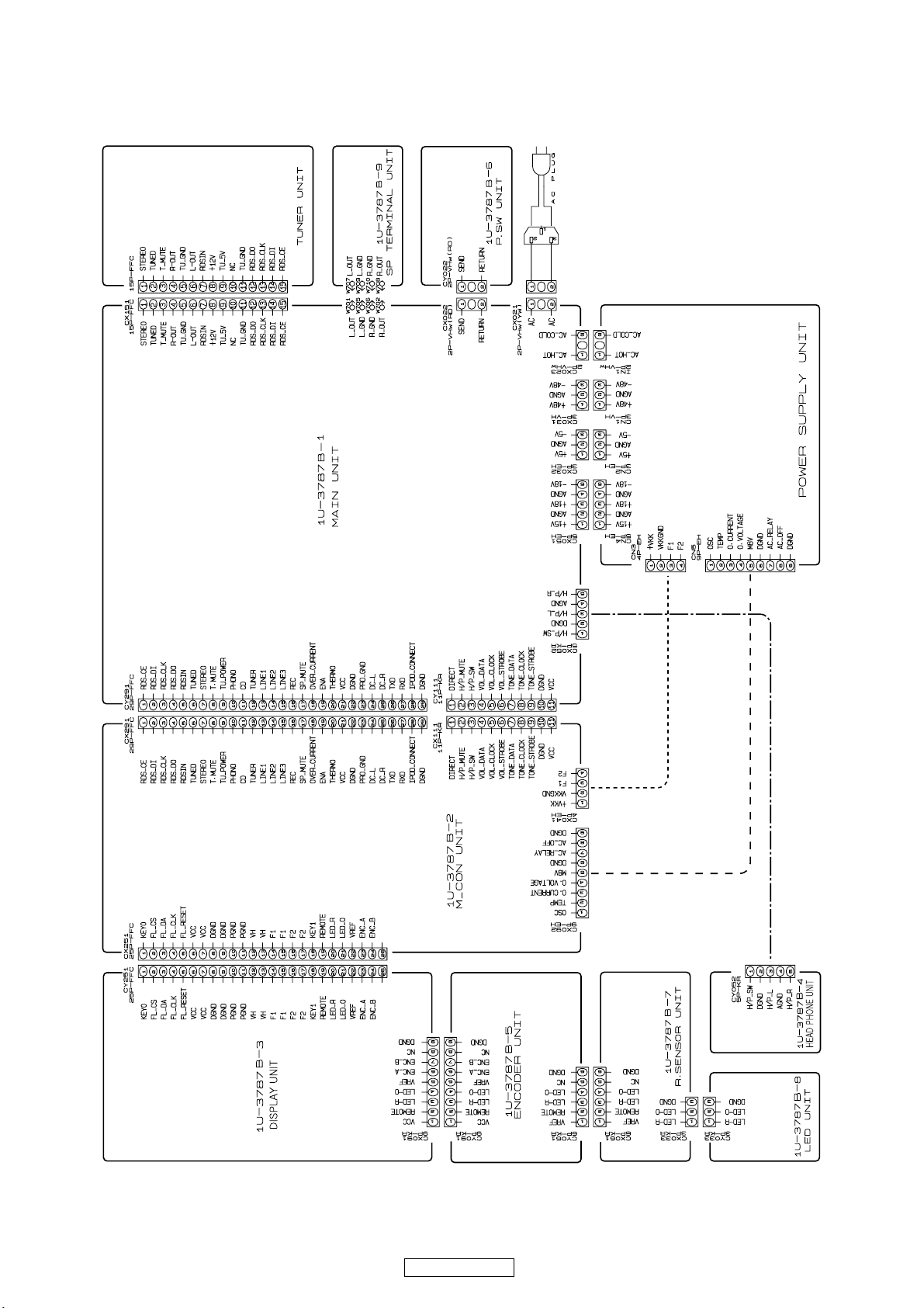
WIRING DIAGRAM
7
DRA-CX3
Page 8
SEMICONDUCTORS / 半導体一覧表
Only major semiconductors are shown, general semiconductors etc. are omitted to list.
主な半導体を記載しています。汎用の半導体は記載を省略しています。
IC's
M3062LFGPGP (IC501)
3
T
/IN
2
11
1
13
/D
/D
/D
3
4
5
1
P1
P
P1
REF
76
10
77
9
78
8
79
7
80
6
81
5
82
4
83
3
84
2
85
1
0
86
87
3
88
2
89
1
90
0
91
3
92
2
93
1
94
SS
95
0
96
97
98
4
99
4
00
1
1 2 3 4 5 6 7 8 9 10111213141516171819202122232425
P12/D
P11/D
P10/D
P07/AN07/D
P06/AN06/D
P05/AN05/D
P04/AN04/D
P03/AN03/D
P02/AN02/D
P01/AN01/D
P00/AN00/D
P107/AN7/KI
P106/AN6/KI
P105/AN5/KI
P104/AN4/KI
P103/AN
P102/AN
P101/AN
AV
P100/AN
V
AVcc
P97/AD
TRG/SIN
6
/ANEX1/S
P9
P95/ANEX0/CLK4
OUT
)
)
)
)
)
0
1
2
3
4
/D
/D
/-)
/D
/D
/D
1
2
0
3
4
5
(/D
(/D
(/D
(/D
(/D
1
/A
1
2
/AN
1
2
P
2
/A
22
/AN
2
P2
3
/A
23
/AN
3
P2
4
/A
4
2
/AN
4
2
P
(/D
5
/A
25
/AN
5
P2
4
5
0
T
T
/A
/IN
/IN
20
14
15
/AN
/D
/D
0
6
7
1
P2
P
P1
M16C/62P Group
)
5
/D
6
(/D
6
/A
26
/AN
6
2
P
)
6
/D
7
(/D
7
/A
7
2
/AN
7
P2
)
7
5
1
2
(/-/D
8
/A
0
CC2
SS
3
V
V
P
3
4
1
16
9
10
1
1
/A
/A
/A
/A
1
2
3
4
P3
P3
P3
P3
57585960616263646566676869707172737475
17
1
1
/A
/A
/A
/A
/A
7
0
1
5
6
P3
P4
P4
P3
P3
515253545556
50
P42/A
49
48
47
46
45
44
43
42
41
40
39
38
37
36
35
34
33
32
31
30
29
28
27
26
18
P43/A
19
P44/CS0
P45/CS1
P46/CS2
P47/CS3
P50/WRL/WR
P51/WRH/BHE
P5
2
/RD
P53/BCLK
P54/HLDA
P55/HOLD
P56/ALE
P57/RDY/CLK
P60/CTS0/RTS
P61/CLK
P62/RxD0/SCL
P63/TXD0/SDA
P64/CTS1/RTS1/CTS0/CLKS
P65/CLK
P66/RxD1/SCL
P67/TXD1/SDA
P7
P7
P72/CLK2/TA1
OUT
0
0
0
0
1
1
1
0/TXD2
/SDA2/TA0
OUT
OUT
(Note)
/V
1
/RxD2/SCL2/TA0IN/TB5IN(Note)
1
BLOCK DIAGRAM
Port P08Port P18Port P28Port P38Port P48Port P58Port P6
Internal peripheral functions
Timer (16-bit)
Output (timer A): 5
Input (timer B): 6
Three-phase motor
control circuit
Watchdog timer
(15 bits)
DMAC
(2 channels)
D-A converter
(8bitsX2channels)
3
3
IN
/TB4
1
/DA
4
P9
IN
/TB3
0
/DA
3
9
P
OUT
/S
IN
/TB2
2
P9
<V
CIN
IN
/S
IN
/TB1
1
P9
CC2
Expandable up to 26 channels)
CRC arithmetic circuit (CCITT )
COUT
/X
BYTE
7
/CLK3
/X
CNVss
RESET
6
IN
P8
P8
/TB0
0
P9
ports>
A-D converter
(10 bitsX8 channels
UART or
clock synchronous serial I/O
(8 bitsX3 channels)
(Polynomial : X
16+X12+X5
M16C/60 series16-bit CPU core
R0LR0H
R1H R1L
R2
R3
A0
A1
FB
OUT
X
IN
SS
X
CC1
V
/NMI
V
/INT
5
4
P8
P8
/INT
3
P8
/INT
2
8
P
IN
/TA3
7
P7
OUT
/TA3
6
7
P
/W
IN
/TA2
5
P7
/W
OUT
/TA2
4
P7
/V
IN
/TA1
2
/RTS
2
/CTS
3
P7
/U
/U
IN
4
OUT
/TA
1
/TA4
0
P8
P8
0
1
2
8
<V
CC1
ports>
Port P7
8
System clock generator
X
PLL frequency synthesizer
Clock synchronous serial I/O
+1)
IN-XOUT
X
CIN-XCOUT
Ring oscillator
(8 bitsX2 channels)
<V
CC1
ports>
Port P8
7
Port P8
5
Memory
Port P9
8
Port P10
8
INTB
PC
SB
USP
ISP
FLG
ROM
(Note 1)
RAM
(Note 2)
Multiplier
<V
CC1
ports> <V
Port P118Port P14
(Note 3) (Note 3)
2
CC2
ports>
Port P128Port P13
(Note 3)
(Note 3)
8
Note 1: ROM size depends on microcomputer type.
Note 2: RAM size depends on microcomputer type.
Note 3: Ports P11 to P14 exist only in 128-pin version.
8
DRA-CX3
Page 9

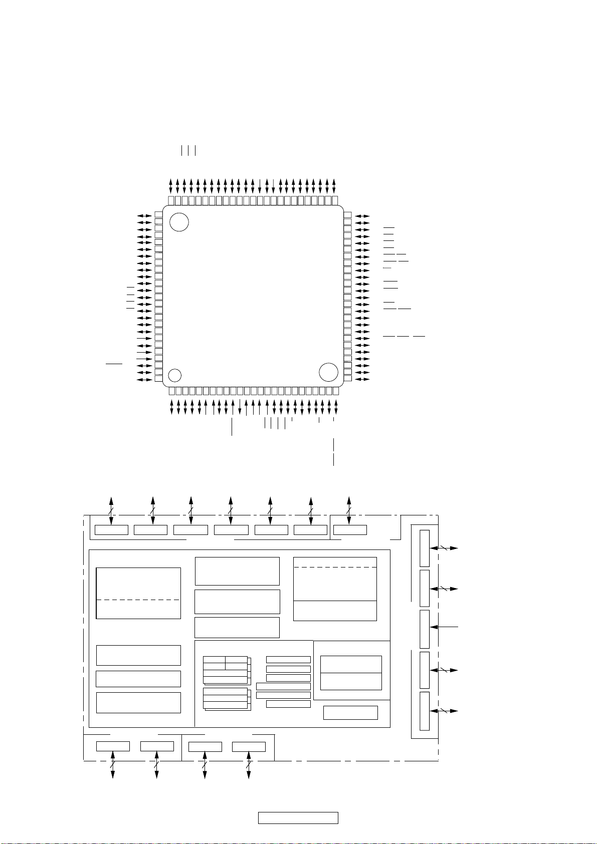
Terminal Function
Pin No. Port Name I/O Initial Function
1 NC O - Not Used.
2 FL_RESET O L Reset output to driver built into FL display tube.
3 TONE_DATA O L Data output to TC9184AP. (20bit)
4 TONE_STROBE O L Strobe output to TC9184AP.
5 TONE_CLOCK O L Clock output to TC9184AP. (below 500kHz)
6 BYTE I - External data bus width switching input. (GND : Single chip mode)
7 CNVSS I - Processor mode switching input. (GND : Single chip mode, PULL DOWN)
8 NC O L Not Used.
9 NC O L Not Used.
10 RESET I - Reset input.
11 XOUT O - Oscillator output. (16 MHz)
12 VSS I - GND.
13 XIN I - Oscillator output. (16 MHz)
14 VCC1 I - Power supply.
15 NC I - Not used. (PULL UP)
16 O.CURRENT/
O.VOLTAGE
17 AC OFF I - Power failure detection input.
18 DBRXD I - Not used. (GND)
19 OSC O L Oscillation frequency control output of power supply unit.
20 H/P_SW I - Headphones connected/disconnected detection input.
21 ENC_B I - Rotary encoder B terminal input.
22 ENC_A I - Rotary encoder A terminal input.
23 FL_CS O L Chip selection output to driver built into FL display tube.
24 LED_O O L Power LED control signal output. ( Orange, STANDBY, H:turn on)
25 LED_R O L Power LED control signal output. (Red, POWER ON, H:turn on)
26 DABCLK O L Not used.
27 DABRXD I - Not used. (GND)
28 DABTXD O L Not used.
29 IPOD_TX O L Data output to i-Pod. (Use even when updating program.)
30 IPOD_RX I - Data input from i-Pod. (Use even when updating program.)
31 NC O L Not used.
32 NC O L Not used. (Terminal for RDS test)
33 S1_DIN I - GND. (DAB ready communication input)
34 S1_DOUT O L Not used. (DAB ready communication output)
35 NC O L Not used.
36 NC O L Not used.
37 NC O L Not used.
38 NC O L Not used.
39 EPM O L Use for updating program.
40 E2P_CLK O L Clock output to EEPROM.
41 E2P_DO I - Data input from EEPROM.
42 E2P_DI O L Data output to EEPROM.
43 E2P_CS O L Chip selection output to EEPROM.
44 CE O L Use for updating program.
45 NC O L Not used.
46 NC O L Not used.
47 PWB_CHECK I - PWB checking mode input.
48 PWB_CHECK I - PWB checking mode input.
49 PWB_CHECK I - PWB checking mode input.
50 PWB_CHECK I - PWB checking mode input.
51 NC O L Not used.
52 NC O L Not used.
53 NC O L Not used.
54 PHONO O L Output for input selection relay. (H : select PHONE)
55 CD O L Output for input selection relay. (H : select CD)
56 LINE1 O L Output for input selection relay. (H : select LINE1)
57 LINE2 O L Output for input selection relay. (H : select LINE2)
I - Overcurrent / overvoltage detection input of power supply unit.
(Low pulse of a microsecond or more .)
(Use for updating program.)
(Active : Low edge)
9
DRA-CX3
Page 10

Pin No. Port Name I/O Initial Function
58 LINE3 O L Output for input selection relay. (H : select LINE3)
59 TU_POWER O L Tuner power ON/OFF control. (H : Tuner ON)
60 VCC I - Power supply.
61 TUNER O L Output for input selection relay. (H : select TUNER)
62 VSS I - GND.
63 RDS_RST O L Reset output to RDS IC.
64 STEREO I - Tuner stereo signal detection input.
65 TUNED I - Tuner reception detection input.
66 T.MUTE O L Tuner MUTE output.
67 RDS_CE O L Chip enable output to tuner RDS IC.
68 RDS_DATA O L Data output to tuner RDS IC.
69 RDS_CLK O L Clock output to tuner RDS IC.
70 RDS_DO I - Data input from tuner RDS IC.
71 Not used I - GND. (Not used)
72 PROTECT I - Power Amp. Error detection input.
73 REMOTE I - IR remote controller input.
74 IPOD_CONNECT I - i-Pod connected/disconnected detection input. (H : Connected)
75 IPOD_POWER O L i-Pod power supply ON/OFF control output.
76 ENA O L Signal output to stop oscillator of Power Amp.
77 SP_MUTE O L SP MUTE output. (H: MUTE ON)
78 DIRECT O L SOURCE DIRECT RELAY control output.
79 H/P_MUTE O L Headphone MUTE output. (H: MUTE ON)
80 AC_RELAY O L Power ON/OFF control. (H : Tuner ON)
81 NC O L Not used.
82 REC O L REC MUTE output. (H: MUTE ON)
83 VOL_DATA O L Data output to TC94A32FG. (24bit)
84 VOL_CLOCK O L Clock output to TC94A32FG. (below 1MHz)
85 VOL_STROBE O L Strobe output to TC94A32FG.
86 NC O L Not used.
87 THERMO I - Power Amp. Overheating detection input.
88 USA O L Not Used.
89 EURO I - Product destination selection input. (JAPAN : L, EURO : H)
90 TEMP I - Power unit overheating detection input.
91 FREQ I - TUNER's skip frequency switching input.
92 RDS I - RDS YES/NO selection input. (H : YES, L : NO)
93 KEY0 I(AD) - Main unit's operating button detection input.
94 AVSS I - GND for AD converter.
95 KEY1 I(AD) - Main unit's operating button detection input.
96 VREF I - Reference voltage input for AD converter and DA converter.
97 AVCC I - Power supply of AD converter.
98 NC O L Not used.
99 FL_DA O L Serial data output to driver built into FL display tube.
100 FL_CLK O L Serial clock output to driver built into FL display tube.
10
DRA-CX3
Page 11
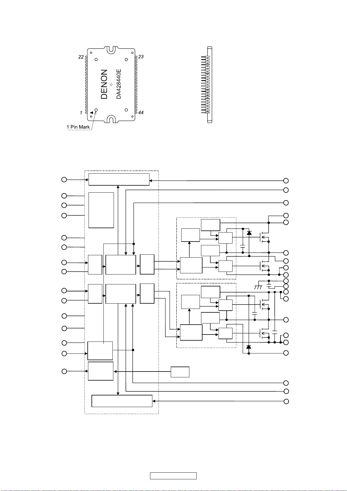
DA428440E-E (IC702)
d
BLOCK DIAGRAM
Control chip
OCM 6
VDCK 10
VSCK 8
DCG 7
ENA 4
TEST 19
IN1- 17
AGND1- 16
Non-inverting
IN2+ 15
AGND2+ 14
VDD 22
AGND
1,9,12,21
VSS 2,11,20
SYN 5
Inverting
Current Prot / HF Prot
Voltage
check
Rec.
Soft
Limit
Rec.
Soft
Limit
COM/MECC
Control ch1
COM/MECC
Control ch2
Shnchro
Circuit
Comp
arator
Comp
arator
Driver chip1
Level
shift
Reciever
DeadTime
Level
shift
Reciever
DeadTime
Driver chip2
Current
etect
Current
detect
Current
detect
Current
detect
High
drive
Low
drive
High
drive
Low
drive
25 ZB1
23 FB1
32 PWMFB1
27 VD1
28 VD1
31 PWM1
26 VDR1
29 VS1
30 VS1
33 SUB
34 VS
36 VD2
37 VD2
40 PWM2
38 VS2
39 VS2
35 VDR2
THM 3
NC
13,18,24,43
Thermal
Warning
Current Prot / HF Prot
NTC
41 PWMFB2
44 FB2
42 ZB2
11
DRA-CX3
Page 12

Terminl Function
Pin No. Pin Name Function
1 AGND Analog ground for control chip power supply.
2 VSS Negative power supply for control chip (-5V).
3 THM Thermal Monitor
Error signal of open collector output “L” for two conditions.
1. Over temperature limitation.
2. Over temperature warning. By connecting to the ENA pin, thermal shutdown is set.
4 ENA Bi-direction input/output.
The input “H” enables to start switching and the input “L” disables.
Input is including hysteresis for glitch free enable of the system.
When the protection circuit detects the over voltage condition, the open collector output turns on.
5 SYN The switching frequency can be synchronized with frequency of this pin signal to avoid the influence
6 OCM Over Current Monitor
7 DCG This high impedance output generates a current in case of over voltage condition on the power stage
8 VSCK This high impedance input for monitoring negative power stage.
9 AGND Analog ground for control chip power supply.
10 VDCK This high impedance input for monitoring positive power stage.
11 VSS Negative power supply for control chip (-5V).
12 AGND Analog ground for control chip power supply.
13 NC
14 AGND2 Input reference for channel 2.
15 IN2+ High impedance audio input for channel 2.
16 AGND1 Input reference for channel 1.
17 IN1- High impedance audio input for channel 1.
18 NC
19 TEST Test terminal connect to VSS.
20 VSS Negative power supply for control chip (-5V).
21 AGND Analog ground for control chip power supply.
22 VDD Positive power supply for control chip (+5V).
23 FB1 Feedback for global loop of channel 1.
24 NC
25 ZB1 For estimating the power dissipation in the zobel resister,
26 VDR1 Positive supply for driver chip of channel 1 with respect to VS1; (VS1+10V).
27 VD1 Positive supply for power stage of channel 1.
28 VD1 Positive supply for power stage of channel 1.
29 VS1 Negative supply for power stage of channel 1.
30 VS1 Negative supply for power stage of channel 1.
31 PWM1 PWM output of channel 1.
32 PWMFB1 Feedback for inner loop of channel 1.
33 SUB Substrate of IMST.
34 VS Negative supply for power stage.
35 VDR2 Positive supply for driver chip of channel 2 with respect to VS2;(VS2+10V).
36 VD2 Positive supply for power stage of channel 2.
37 VD2 Positive supply for power stage of channel 2.
38 VS2 Negative supply for power stage of channel 2.
39 VS2 Negative supply for power stage of channel 2.
40 PWM2 PWM output of channel 2.
41 PWMFB2 Feedback for inner loop of channel 2.
42 ZB2 For estimating the power dissipation in the zobel resister,
43 NC
44 FB2 Feedback for global loop of channel 2.
for AM radio tuner.
Normal condition is “L”.
Error signal of open collector output “L” for two conditions.
1. Over current limitation.
2. For monitoring the state of control and average voltage across the zobel resistor in case of of-limit
conditions.
voltage (VD/VS).
This current is designed to turn-on a set of discharge transistors.
This monitoring controls the soft clipping circuit and the over voltage shutdown.
This monitoring controls the soft clipping circuit and the over voltage shutdown.
This is true inverting low impedance (1kohm) input for avoiding ground loop noise.
This input is non-inverting.
This is true non-inverting low impedance (2kohm) input for avoiding ground loop noise.
This input is inverting.
this input is sensing the zobel voltage via a resistive network of channel 1.
this input is sensing the zobel voltage via a resistive network of channel 2.
12
DRA-CX3
Page 13
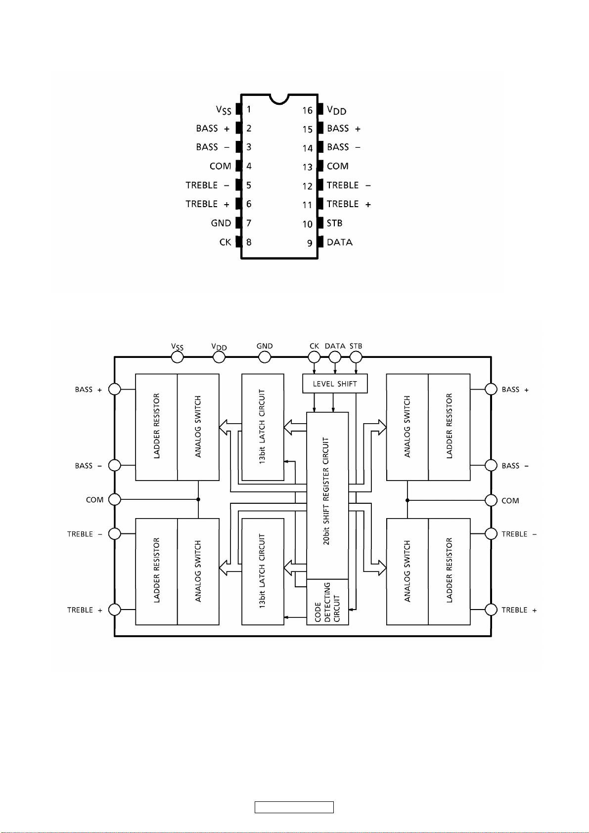
TC9184AP (IC307)
PIN CONNECTION
BLOCK DIAGRAM
13
DRA-CX3
Page 14

TC94A32F (IC306)
TC74VHCT08AFT (IC504)
TC74LCX08FT (IC602)
14
DRA-CX3
Page 15

BA05FP (IC502)
BA033FP (IC601)
1: Vcc
2: N.C.
3: Vout
2
1
3
FIN: GND
BR93L86RFVM-WTR (IC505)
SA5532ADR (IC301)
OP275GSR (IC302)
NJM2068MD-TE1 (IC303)
OPA2134UA (IC304,701)
NJM4556AD (IC305)
NJM082D (IC401)
A OUTPUT
A –INPUT
A+INPUT
V
1
1
2
3
4
8
7
2
6
5
V
B OUTPUT
B –INPUT
B+INPUT
15
DRA-CX3
Page 16

NJM7812FA(SS)-#4MS (IC202)
GP1UM271XK (IC503)
Vcc
Vout
GND
LC72722PM-TLM-E (IC201)
Pin Assignment
Head
Amp
REF
Limiter
Amp
BPF
124V
223MPXIN CE
322Vdda DI
421Vssa CL
520FLOUT DO
619CIN
718T1 SYNC
817T2 T7
916T3 T6
10 15T4 Vssd
11 14T5 Vddd
12 13X
OUT
Detector &
Comparator
SYR
RDS-ID
X
Integrator
IN
Hysteresis
Comparator
GND
Vcc
Vout
Block Diagram
+5V +5V
Vdda
Vssa
MPXIN
DO
CL
DI
CE
T1
T2
T3 to T7
REFERENCE
VOLTAGE
ANTIALIASING
FILTER
CCB
TEST
V
REF
57 kHz
BPF
(SCF)
(24 BLOCK DATA)
MEMORY CONTROL
SMOOTHING
FILTER
RAM
Top view
CINFLOUT
+
-
V
REF
ERROR CORRECTION
(SOFT DECISION)
CLK(4.332 MHz)
OSC/DIVIDER
X
IN
(57 kHz)
X
OUT
PLL
SYNC/EC CONTROLLER
SYNC
DETECT-1
CLOCK
RECOVERY
(1187.5 Hz)
DATA
DECODER
DETECT-2
Vddd
Vssd
RDS-ID
SYNC
SYR
SYNC
16
DRA-CX3
Page 17

ı
TRANSISTORS
KTA1268BL
KTC3200BL
FRONT
VIEW
C
B
E
2SA1837 (Y)
2SC4793 (Y)
FRONT
VIEW
BCE
DIODES (LED included)
1SS270A
1SR139-400
MTZJ3.3A
MTZJ5.6A
MTZJ16A
MTZJ18A
HZS11B-1
2SK170 (BL)2SK373 (Y)
2SK369 (BL/GR)-C
FRONT
VIEW
G
S
D
FRONT
VIEW
DGS
SLI-343DU3F (ORG) SLA-360LT3F (XE)
1SR35-400A
DTA114TK
DTA114EK
PNP Type
2SC4672 KDS160
(1) Base
(2) Collector
(3) Emitter
(2)
(3)
(1)
DTC114EK
DTC114TK
DTC114YK
DTC144EK
DTC323TK
NPN Type
R1
B
R2
2SA1037K(S/R)
2SC2412K(S)
2
1
3
C
E
1:Emitter
2:Base
3:Collector
1
3
1:Emitter
2:Base
3:Collector
2
DTA114EK
DTC114EK
DTC144EK
DTC114YK
DTC323TK
DTA114TK
DTC114TK
R1
10kohm
10kohm
4.7kohm 47kohm
10kohm
2.2kohm
10kohm
10kohm
R2
10kohm
10kohm
47kohm
17
DRA-CX3
Page 18

FL DISPLAY
8BT258GINK (FL 601)
PIN CONNECTION
GRID ASSIGNMENT SEGMENT DESIGNATION
ANODE CONNECTION
18
DRA-CX3
Page 19

PRINTED WIRING BOARD
1U-3787 MAIN P.W.B. UNIT (E2 model only)
COMPONENT SIDE
d
19
DRA-CX3
Page 20

1U-3787 MAIN P.W.B. UNIT (E2 model only)
FOIL SIDE
20
DRA-CX3
Page 21

8U-210023 MAIN P.W.B. UNIT (E3 model only)
d
COMPONENT SIDE
21
DRA-CX3
Page 22

8U-210023 MAIN P.W.B. UNIT (E3 model only)
d
FOIL SIDE
22
DRA-CX3
Page 23

NOTE FOR PARTS LIST
• Part indicated with the mark "nsp" are not always in stock and possibly
to take a long period of time for supplying, or in some case supplying
of part may be refused.
• When ordering of part, clearly indicate "1" and "I" (i) to avoid mis-
supplying.
• Ordering part without stating its part number can not be supplied.
• Pa rt i ndi cat ed w ith the mar k " ★" is not illustrated in the exploded view.
• Not including General-purpose Carbon Film Resistor in the P.W.Board
parts list. (Refer to the Schematic Diagram for those parts.)
• Not including General-purpose Carbon Chip Resistor in the P.W.Board
parts list. (Refer to the Schematic Diagram for those parts.)
WARNING:
Parts marked with this symbol z have critical characteristics.
Use ONLY replacement parts recommended by the manufacturer.
部品表について
1.nsp 印の部品は常時在庫していませんので供給に長時間を要するこ
とがあります。
場合によっては、供給をお断りすることがあります。
2.部品を発注する際は特に数字の " 1 " と英字の "I" との区別をはっ
きり記入してください。
3.部品番号を表示していない部品は供給できません。
4.z印の部品は安全上重要な部品です。交換するときは、安全およ
び性能維持のため必ず指定の部品をご使用ください。
5.★印のついている部品は分解図中には記載していません。
6.汎用カーボン抵抗器は記載していません。定数は回路図を参照願い
ます。
7.汎用カーボンチップ抵抗器は記載していません。定数は回路図を参
照願います。
8.部品表の抵抗器、コンデンサの品名記号の読み方は表を参照してく
ださい。
23
DRA-CX3
Page 24

PARTS LIST OF P.W.B. UNIT
*本表に記載されている部品は、補修用部品のため製品に使用している部品とは一部、形状、寸法などが異なる場合があります。
* The parts listed below are for maintenance only, might differ from the parts used in the unit in appearances or dimensions.
*"nsp" 印の部品は常時在庫していませんので供給に長時間を要することがあります。場合によっては、供給をお断りする場合があります。
* Part indicated with the mark “nsp” are not always in stock and possibly to take a long period of time for supplying, or in some case supplying of part may be refused.
Note: The symbols in the column "Remarks" indicate the following destinations.
E3 : U.S.A. & Canada model E2 : Europe model
1U-3787 B MAIN P.W.B. UNIT ASSY : for E2
8U-210023 MAIN P.W.B. UNIT ASSY : for E3
Ref. No. nsp Part No. Part Name Remarks Q'ty New
SEMICONDUCTORS GROUP
IC201 00D 262 3657 906 LC72722PM-TLM-E
IC202 00D 263 1179 049 NJM7812FA(SS)-#4MS
IC301 00D 262 3555 901 SA5532ADR
IC302 00D 263 1074 908 OP275GSR +C
IC303 00D 263 0896 909 NJM2068MD-TE1 +C
IC304 00D 263 1071 901 OPA2134UA +C
IC305 00D 263 0995 004 NJM4556AD +T
IC306 00D 262 3168 903 TC94A32F +C
IC307 00D 262 2616 003 TC9184AP
IC401 00D 263 0244 001 NJM082D
IC501 00D GEN 8675-1 PROGRAM WRITING SUB M3062LFGPGP *
IC502 00D 263 1078 904 BA05FP +C
IC503 00D 499 0303 004 GP1UM271XK
IC504 00D 262 3410 907 TC74VHCT08AFT
IC505 00D 262 3498 903 BR93L86RFVM-WTR
IC601 00D 263 1079 903 BA033FP +C
IC602 00D 262 3488 900 TC74LCX08FT
IC701 00D 263 1071 901 OPA2134UA +C
IC702 00D 264 0001 001 DA428440E-E *
ご注意:
ファームウエアをアップデート
するときは、SDI で最終バージョ
ンを確認して下さい。
サービス基板はアップデートし
て使用下さい。
NOTE :
When update Firmware, please
confirm a last version in SDI.
Use the service board after
updating it.
d
d
sd
TR201-209 00D 269 0144 905 DTC114YK-T146 +C
TR211,212 00D 269 0066 902 DTC323TKT96 +C
TR213 00D 269 0086 908 DTA114TKT96 +C
TR214,215 00D 269 0082 902 DTC114EKT96 +C
TR216 00D 273 0384 900 2SC2412KT96(S) +C
TR217 00D 272 0161 900 2SB1412TL(PQR) +C
TR218 00D 269 0082 902 DTC114EKT96 +C
TR401-404 00D 275 0038 045 2SK369 (BL)/(GR)-C
TR503,504 00D 273 0384 900 2SC2412KT96(S) +C
TR505 00D 272 0161 900 2SB1412TL(PQR) +C
TR506 00D 269 0082 902 DTC114EKT96 +C
TR508 00D 269 0083 901 DTA114EKT96 +C
TR509 00D 269 0082 902 DTC114EKT96 +C
TR510 00D 273 0384 900 2SC2412KT96(S) +C
TR511 00D 271 0238 908 2SA1037KT146S +C
TR512,513 00D 273 0384 900 2SC2412KT96(S) +C
TR514 00D 271 0238 908 2SA1037KT146S +C
TR515 00D 273 0384 900 2SC2412KT96(S) +C
TR516 00D 269 0054 901 DTC144EKT96 +C
TR517,518 00D 273 0384 900 2SC2412KT96(S) +C
TR601 00D 273 0463 902 2SC4672T100PQ +C
TR603,604 00D 269 0088 906 DTC114TKT96 +C
TR701 00D 273 0423 007 2SC4793-Y
TR702 00D 271 0272 003 2SA1837-Y
TR703,704 00D 275 0060 903 2SK-170BL(TPE2)
TR705 00D 273 0458 904 KTC3200-BL-AT/P
TR706 00D 271 0301 903 KTA1268-BL-AT/P
TR707 00D 275 0042 905 2SK373(Y)TPE2
24
DRA-CX3
Page 25

Ref. No. nsp Part No. Part Name Remarks Q'ty New
TR708 00D 273 0423 007 2SC4793-Y
TR709 00D 269 0144 905 DTC114YK-T146 +C
D201-209 00D 276 0432 903 1SS270A TE (TAPE)
D401,402 00D 276 0432 903 1SS270A TE (TAPE)
D501,502 00D 276 0704 903 1SR35-400A(T93X)
D503-505 00D 276 0794 900 KDS160-RTK/P
D506-508 00D 276 0833 900 ESD PROTECTOR(6802)
D509-514 00D 276 0794 900 KDS160-RTK/P
D515 00D 276 0704 903 1SR35-400A(T93X)
D516,517 00D 276 0794 900 KDS160-RTK/P
D601-603 00D 276 0796 908 1SR139-400T-31
D701 00D 276 0432 903 1SS270A TE (TAPE)
ZD501 00D 276 0634 905 MTZJ3.3AT77
ZD502 00D 276 0643 996 MTZJ5.6A T77
ZD601,602 00D 276 0645 907 MTZJ18A T77
ZD701,702 00D 276 0644 995 MTZJ16A T77
ZD703 00D 276 0471 906 HZS11B-1TD
LD602 00D 393 9656 001 SLI343DU3F (ORG)
LD603 00D 393 9667 003 SLA-360LT3F(XE) *
PH701,702 00D 279 0052 007 NTPAD8R0LDNB0 *
FL601 00D 393 8093 005 FL TUBE(8BT258GINK) *
RESISTORS GROUP
R361,362 00D 244 2051 961 RS14B3A101JNBST(S)
R363,364 00D 244 2051 974 RS14B3A102JNBST(S)
R365-368 00D 244 2052 928 RS14B3A470JNBST(S)
R539 00D 244 2051 961 RS14B3A101JNBST(S)
R547,548 00D 241 2387 908 RD14B2E010JNBST
R601 00D 241 2387 908 RD14B2E010JNBST
R620,621 00D 241 2314 049 RD14B2E100JNBF
R710,711 00D 241 2315 912 RD14B2E100GFRST
R718 00D 241 2381 946 RD14B2E472JNBST
R723 00D 241 2381 946 RD14B2E472JNBST
R726 00D 241 2376 964 RD14B2E470JNBST
R728,729 00D 243 2095 018 RW99A4A4R7K *
R732 00D 244 2051 961 RS14B3A101JNBST(S)
R737,738 00D 243 2095 021 RW99A4A202K *
CAPACITORS GROUP
z C101 00D 253 8022 707 CK45F2EAC103MC
C201,202 00D 254 4573 994 CE04W1H220MT(RA3)
C203 00D 254 4703 751 CE04W1H220MC(RFS#A)
C204-208 00D 254 4573 994 CE04W1H220MT(RA3)
C209 00D 254 4703 751 CE04W1H220MC(RFS#A)
C221-225 nsp 00D 257 0509 929 CK73B1H102KT +1608
C227,228 nsp 00D 257 0509 929 CK73B1H102KT +1608
C230 nsp 00D 257 0506 951 CC73CH1H101JT +1608
C233 00D 254 4573 981 CE04W1H100MT(RA3)
C234 00D 254 4696 981 CE04W1H100MT(R2A)
C235 00D 254 4696 949 CE04W1H010MT(R2A)
C236 nsp 00D 257 0516 954 CK73B1E104KT +1608
C237 nsp 00D 257 0507 976 CC73CH1H331JT +1608
C238 nsp 00D 257 0508 933 CC73CH1H561JT +1608
C239,240 nsp 00D 257 0504 908 CC73CH1H220JT +1608
C241,242 00D 254 4702 956 CE04W1H100MT(RFS#A)
25
DRA-CX3
Page 26

Ref. No. nsp Part No. Part Name Remarks Q'ty New
C301,302 00D 255 4254 915 CQ93P2A102JT(NH2)
C305,306 00D 254 4703 751 CE04W1H220MC(RFS#A)
C307-310 00D 254 4702 956 CE04W1H100MT(RFS#A)
C311,312 00D 254 4777 716 CE04W1H470MC(RGO#A) *
C313,314 00D 254 4702 943 CE04W1H4R7MT(RFS#A)
C315,316 00D 255 4250 964 CQ93P2A330JT(NH2)
C317-319 nsp 00D 257 0509 929 CK73B1H102KT +1608
C321,322 00D 254 4573 981 CE04W1H100MT(RA3)
C323,324 00D 254 4573 965 CE04W1H3R3MT(RA3)
C325,326 00D 255 4251 976 CQ93P2A101JT(NH2)
C327,328 00D 254 4573 978 CE04W1H4R7MT(RA3)
C329,330 00D 255 1265 923 CQ93M1H822JT(B)
C331,332 00D 256 1058 942 CF93A1H563JT (JL)
C333,334 00D 255 1264 937 CQ93M1H182JT(B)
C335,336 00D 255 1265 949 CQ93M1H123JT(B)
C337,338 00D 254 4573 978 CE04W1H4R7MT(RA3)
C339,340 00D 254 4573 994 CE04W1H220MT(RA3)
C341,342 00D 254 4702 956 CE04W1H100MT(RFS#A)
C343 nsp 00D 257 0509 929 CK73B1H102KT +1608
C355,356 00D 254 4569 924 CE04W1E101MT(RA3)
C357,358 00D 255 4252 959 CQ93P2A221JT(NH2)
C359 00D 255 4254 957 CQ93P2A152JT(NH2)
C403,404 00D 255 4252 917 CQ93P2A151JT(NH2)
C405,406 00D 255 4254 915 CQ93P2A102JT(NH2)
C409,410 00D 255 4255 930 CQ93P2A332JT(NH2)
C411-414 00D 254 4699 904 CE04W1E101MT(R2A)
C415,416 00D 254 4696 981 CE04W1H100MT(R2A)
C417,418 00D 255 4254 931 CQ93P2A122JT(NH2)
C419,420 00D 255 4257 912 CQ93P2A183JT(NH2)
C421,422 00D 255 4259 716 CQ93P2A683JFC(NH2)
C423,424 00D 255 4254 915 CQ93P2A102JT(NH2)
C425,426 00D 254 4699 904 CE04W1E101MT(R2A)
C427,428 00D 254 4702 956 CE04W1H100MT(RFS#A)
C429 00D 255 4256 955 CQ93P2A103JT(NH2)
C430 00D 257 0505 910 CC73CH1H152JT +1608
C501 00D 254 4696 981 CE04W1H100MT(R2A)
C502,503 nsp 00D 257 0509 929 CK73B1H102KT +1608
C504,505 nsp 00D 257 0506 951 CC73CH1H101JT +1608
C506 nsp 00D 257 0501 901 CK73B1H103KT (1608) +1608
C511 00D 255 1279 951 CQ93M1H104JT(B)
C512 00D 254 4696 978 CE04W1H4R7MT(R2A)
C513,514 nsp 00D 257 0501 901 CK73B1H103KT (1608) +1608
C515 nsp 00D 257 0509 929 CK73B1H102KT +1608
C516 00D 254 4789 704 CE04W1A332MC(RA3)
C517 00D 254 4577 958 CE04W1C221MT(RA3)
C518 nsp 00D 257 0509 929 CK73B1H102KT +1608
C520 nsp 00D 257 0516 954 CK73B1E104KT +1608
C521 00D 254 4577 961 CE04W1C331MT(RA3)
C522 nsp 00D 257 0516 954 CK73B1E104KT +1608
C523 00D 254 4577 961 CE04W1C331MT(RA3)
C524 00D 254 4699 904 CE04W1E101MT(R2A)
C525 00D 254 4703 777 CE04W1H470MC(RFS#A)
C526 00D 254 4696 936 CE04W1HR47MT(R2A)
C530 00D 257 3012 921 CF73=1H103JT(ECHUB5)+3216
C531 nsp 00D 257 0509 929 CK73B1H102KT +1608
C532 00D 254 4696 981 CE04W1H100MT(R2A)
C533,534 nsp 00D 257 0516 954 CK73B1E104KT +1608
C535 nsp 00D 257 0509 929 CK73B1H102KT +1608
C536 00D 257 0505 910 CC73CH1H152JT +1608
C542 00D 254 4574 919 CE04W1H470MT(RA3)
C543 00D 254 4573 978 CE04W1H4R7MT(RA3)
26
DRA-CX3
Page 27

Ref. No. nsp Part No. Part Name Remarks Q'ty New
C601 00D 254 4702 956 CE04W1H100MT(RFS#A)
C602 00D 254 4703 777 CE04W1H470MC(RFS#A)
C611,612 nsp 00D 257 0516 954 CK73B1E104KT +1608
C613 00D 254 4574 922 CE04W1H101MT(RA3)
C614 00D 254 4699 904 CE04W1E101MT(R2A)
C615-618 nsp 00D 257 0506 951 CC73CH1H101JT +1608
C619 00D 254 4699 904 CE04W1E101MT(R2A)
C620,621 nsp 00D 257 0516 954 CK73B1E104KT +1608
C631,632 nsp 00D 257 0516 954 CK73B1E104KT +1608
C701,702 00D 254 4774 706 CE04W1E101MF(RFS#A)
C705,706 00D 254 4702 956 CE04W1H100MT(RFS#A)
C707,708 00D 255 4257 938 CQ93P2A223JT(NH2)
C709,710 00D 254 4703 777 CE04W1H470MC(RFS#A)
C711,712 00D 254 4777 716 CE04W1H470MC(RGO#A) *
C713-716 00D 255 6188 005 CQ09S2B103J(PPSC)
C717,718 00D 254 6266 005 CE04W1J822M(DL)
C719 00D 257 1022 900 CK73B2A104KT-3216 *
C720-723 00D 257 1022 900 CK73B2A104KT-3216 for E2 *
C720-723 132 550 0175 23S CK73X7R2A684KT for E3 *
C724 00D 257 1022 900 CK73B2A104KT-3216 *
C725,726 00D 256 1069 012 CF93A2E394K(DTDZ) *
C727 00D 257 0505 910 CC73CH1H152JT +1608
C728,729 00D 255 6188 005 CQ09S2B103J(PPSC)
C731 00D 254 4702 956 CE04W1H100MT(RFS#A)
C732,733 00D 256 1069 012 CF93A2E394K(DTDZ) *
C734 00D 254 4703 777 CE04W1H470MC(RFS#A)
C735,736 00D 255 4254 999 CQ93P2A222JT(NH2)
C739,740 00D 255 4250 948 CQ93P2A220JT (NH2)
C751-761 00D 257 0043 919 CK73U2J2E222JT(2125)
C763,764 00D 255 4252 959 CQ93P2A221JT(NH2)
C763,764 00D 257 3010 949 CF73=1H221JT(ECHUB5)
C765,766 00D 255 4254 915 CQ93P2A102JT(NH2)
C765,766 00D 257 3011 919 CF73=1H102JT(ECHUB5)
S.No. 1 〜 200
S.No. 201 〜
S.No. 1 〜 200
S.No. 201 〜
d
d
OTHERS PARTS GROUP
CW034 00D 203 5399 001 3P SCN-SCN CON.CORD *
CX021 nsp 00D 205 1093 006 2P VH CONNECTOR BASA
CX022 nsp 00D 205 0581 069 2P VH CON BASE (Red)
CX023 nsp 00D 205 0581 001 2P VH CON BASE (White)
CX031 nsp 00D 205 0653 036 3P VH CON.BASE
CX032 nsp 00D 205 0233 032 3P EH CONNECTOR BASE
CX033 nsp 00D 205 0355 033 3P KR CON BASE(L)
CX041 nsp 00D 205 0233 045 4P EH CONNECTOR BASE
CX051 nsp 00D 205 0233 058 5P EH CONNECTOR BASE
CX052 nsp 00D 205 0343 058 5P CONN.BASE(KR-PH)
CX061 nsp 00D 205 0355 062 6P KR CON BASE(L)
CX081 nsp 00D 205 0343 087 8P CONN.BASE(KR-PH)
CX091 nsp 00D 205 0343 090 9P CONN.BASE(KR-PH)
CX092 nsp 00D 205 0233 090 9P EH CONNECTOR BASE
CX111 nsp 00D 205 0375 013 11P CON.BASE(KR-PH)
CX151 00D 205 0736 076 15P FFC CON.BASE
CX251 00D 205 1316 000 25P FFC BASE(9610S)Y
CX291 00D 205 1260 046 29P FFC BASE (9610SA
CY022 nsp 00D 205 0581 069 2P VH CON BASE (Red)
CY033 nsp 00D 205 0355 033 3P KR CON BASE(L)
CY052 nsp 00D 205 0343 058 5P CONN.BASE(KR-PH)
CY061 nsp 00D 205 0355 062 6P KR CON BASE(L)
CY091 nsp 00D 205 0355 091 9P KR CON BASE(L)
CY111 nsp 00D 205 0375 013 11P CON.BASE(KR-PH)
27
DRA-CX3
Page 28

Ref. No. nsp Part No. Part Name Remarks Q'ty New
CY251 00D 205 1316 000 25P FFC BASE(9610S)Y
CY291 00D 205 1260 046 29P FFC BASE (9610SA
z F101 00D 206 1046 001 FUSE 6.3AUL 20MM for E3
z F101 00D 206 1100 060 FUSE 4A(HT N5) for E2
z F108 00D 206 1015 032 FUSE (2.5A) for E2
z F108 00D 206 1046 014 FUSE 8A for E3
FB701,702 nsp 00D 247 0018 905 RM73B--0R0KT +2125
FB703 nsp 00D 247 2018 903 RM73B--0R0KT +1608
FF101 nsp 00D 202 0040 909 FUSE CLIP(TAPE)
FF108 nsp 00D 202 0040 909 FUSE CLIP(TAPE)
FH101 nsp 00D 202 0040 909 FUSE CLIP(TAPE)
FH108 nsp 00D 202 0040 909 FUSE CLIP(TAPE)
JK201 00D 204 8531 018 2P PIN JACK (C-GND)
JK202 00D 204 8549 000 2P PIN JACK(18MM)
JK203,204 00D 204 8530 019 4P PIN JACK
JK301 00D 204 8480 004 HEAD PHONE JACK(SW)
JK501 00D 204 8732 008 H/P JACK(D3.5-SW) *
z JK703 00D 203 3961 004 1P AC OUTLET(E2) for E2
z JK701 00D 203 3957 005 AC OUTLET(1P) for E3
L701,702 115 010 0024 00S #C3B-A0376 *
RL201-209 00M LY2 0120 620 ED2-12NU NEC 12V RELAY
RL702 00D 214 0195 006 RELAY FTR-F1
d
sd
d
d
d
d
S101 00D 212 4728 004 1P PUSH SWITCH
z S102 00D 212 1176 002 POWER SWITCH (TV-5)
S601-604 00D 212 5611 903 TACT SWITCH(TAPE H5)
S605 00D 212 0526 006 ROTARY ENCODER(V)
ST101-105 nsp 00D 205 0452 017 STYLE PIN
W301 nsp 00D 203 0535 051 1P CONTACT ASSY
W401 nsp 00D 001 0070 033 VINYL WIRE
W402 nsp 00D 001 0070 020 VINYL WIRE
W501 nsp 00D 205 1034 007 M3 SCREW TERMINAL
W701,702 nsp 00D 205 0864 003 M3 SCREW TERMINAL
W705,706 nsp 00D 205 0864 003 M3 SCREW TERMINAL
W707,708 nsp 00D 203 0765 009 1P CON.ASSY
W709,710 nsp 00D 203 0765 012 1P CON.ASSY
X201 00D 399 0178 007 X-TAL(4.332MHZ)
X501 00D 399 0805 914 CSTLS16M0X51-A0
nsp 00D 417 0706 007 RADIATOR (PUE36) TR708 *
nsp 00D 417 0704 009 RADIATOR IC702 *
nsp 0RD 471 3304 028 3X8 CBS-B
nsp 00D 461 0862 045 FL SPACER (T=5)
nsp 00D 461 0415 007 RUBBER SHEET
nsp 00D 513 4190 001 FUSE LABEL(T4AH) F101, for E2
nsp 00D 513 3730 048 FUSE LABEL(T2.5AL) F108, for E2
nsp - FUSE LABEL (6.3A) F108, for E3
nsp 00D 415 0299 000 CONDENSER COVER C101, for E2
nsp 00D 415 0866 006 CONDENSER COVER C101, for E3
sd
d
d
d
d
28
DRA-CX3
Page 29

EXPLODED VIEW
109
108
d
29
108
1-8
106
28
22
1-7
27
106
56
1-5
1-6
1-4
55
d
90
106
117
45
106
25
32
110
107
106
26
106
24
1-2
33
102
d
89
110
110
19
101
102
d
91
44
17
31
20
115
43
POWER SUPPLY UNIT
113
13
116
44
6
114
35
101
18
36
38
1-9
111
112
37
57
116
11
111
13
112
114
1-1
102
58
103
59
20
39
14
10
102
104
15
2
WARNING:
Parts marked with this symbol have critical
characteristics.
Use ONLY replacement parts recommended by
the manufacturer.
印の部分は安全を維持するために重要
な部品です。従って交換時は必ず指定の
部品を使用してください。
42
RED
8
12
BLUE
9
102
40
102
102
105
102
103
34
102
16
102
7
102
30
41
109
21
23
1-3
102
29
DRA-CX3
53
52
102
5
3
4
31
110
101
Page 30

--MEMO--
30
DRA-CX3
Page 31

PARTS LIST OF EXPLODED VIEW
dddddfdfddd
d
sd
d
ddd
*本表に記載されている部品は、補修用部品のため製品に使用している部品とは一部、形状、寸法などが異なる場合があります。
* The parts listed below are for maintenance only, might differ from the parts used in the unit in appearances or dimensions.
*"nsp" 印の部品は常時在庫していませんので供給に長時間を要することがあります。場合によっては、供給をお断りする場合があります。
* Part indicated with the mark “nsp” are not always in stock and possibly to take a long period of time for supplying, or in some case supplying of part may be refused.
Note: The symbols in the column "Remarks" indicate the following destinations.
E3 : U.S.A. & Canada model E2 : Europe model
Ref. No. nsp Part No. Part Name Remarks Q'ty New
1 - MAIN P.W.B. UNIT ASSY for E3 1 *
1 - MAIN P.W.B. UNIT ASSY for E2 1 *
1-1 MAIN UNIT
1-2 M-CON UNIT
1-3 DISPLAY UNIT
1-4 HEAD PHONE UNIT
1-5 ENCODER UNIT
1-6 P. SW UNIT
1-7 R.SENSOR UNIT
1-8 LED UNIT
1-9 SP TERMINAL UNIT
2 nsp 00D 411 2101 000 MAIN CHASSIS 1 *
3 nsp 00D 104 0352 005 FOOT 4 *
4 nsp 00D 461 0385 001 RUBBER PAD 4
5 nsp 00D 105 1670 103 BOTTOM COVER 2 *
6 nsp 00D 412 2814 028 CARD SPACER(L=10) 1
7 nsp 00D 105 1668 115 BACK PANEL for E2 1 *
7 nsp 00D 105 1668 102 BACK PANEL for E3 1
8 00D 205 1409 001 1P SP TERMINAL RED 2 *
9 00D 205 1410 003 1P SP TERMINAL BLUE 2 *
10 nsp 00D 462 0185 000 SP WASHER (A) 4 *
11 nsp 00D 462 0186 009 SP WASHER (B) 4 *
12 nsp 00D 477 0331 005 PUSH RIVET 4 *
13 nsp 00D 415 0947 006 BUSH 5
z 14 00D 203 3996 008 AC INLET(2P) 1
15 00D 216 0125 001 AM FM TUNER(E2) for E2 1
15 00D 216 0125 108 or FM AM TUNER(E2) for E2 1
15 00D 216 0124 002 AM FM TUNER(E3) for E3 1
15 00D 216 0124 109 or FM AM TUNER(E3) for E3 1
16 nsp 00D 205 1116 006 TERMINAL ASS 1
z 17 00D 399 1081 012 POWER SUPPLY UNIT for E2 1 *
z 17 694 010 0010 09D POWER SUPPLY UNIT for E3 1 *
18 nsp 00D 415 1006 001 INSULATING SHEET 1 *
19 nsp 00D 412 5336 008 FRONT ANGLE 1 *
20 nsp 00D 412 5335 009 TOP PANEL BRACKET 2 *
21 00D 144 2999 215 FRONT PANEL ASSY 1 *
22 nsp 00D 412 5340 007 VOLUME PLATE 1 *
23 00D 113 2056 002 FUNCTION KNOB ASSY 1 *
24 nsp 00D 461 1140 012 PAD 1
25 nsp 00D 461 0957 057 RUBBER FOAM 1
26 nsp 00D 412 2404 030 PWB HOLDER (WLS-16) 1
27 nsp 00D 412 5334 000 POWER KNOB BRACKET 1 *
28 nsp 00D 113 2053 005 POWER KNOB HOLDER 1 *
29 00D 113 2054 004 POWER KNOB ASSY 1 *
30 00D 112 0983 006 KNOB (V) ASSY 1 *
31 00D 144 2993 101 SIDE PANEL 2 *
32 00D 144 2994 016 TOP PANEL(F) 1 *
33 00D 144 2995 015 TOP PANEL(R) 1 *
34 nsp 00D 105 1669 237 BACK PLATE for E2 1 *
34 nsp 00D 105 1669 253 BACK PLATE for E3 1 *
35 nsp 00D 417 0704 009 RADIATOR IC702 1 *
z 36 00D 203 3961 004 AC OUTLET (E2) 1
z 37 00D 206 1100 060 FUSE 4A(HT 5N) F101, for E2 1
z 37 00D 206 1046 001 FUSE 6.3AUL 20MM F101, for E3 1
z 38 00D 206 1015 032 FUSE (2.5A) F108, for E2 1
z 38 00D 206 1046 014 FUSE 8A F108, for E3 1
39 nsp 00D 209 0325 007 SHORT PIN 2
40 nsp 00D 513 1581 008 SERIAL NO. SHEET for E2 1
31
DRA-CX3
Page 32

Ref. No. nsp Part No. Part Name Remarks Q'ty New
d
ddssddd
40 nsp 00D 513 1581 011 SERIAL NO. SHEET for E3 1
41 nsp 00D 461 1288 000 VOLUME SHEET 1 *
42 nsp 00D 342 0044 009 LOW CUT CORE(TRM25) 1
43 nsp 00D 414 1050 009 SHIELD PLATE 1 *
44 nsp 00D 415 1008 009 INSULATING SHEET 2 *
45 nsp 00D 461 1182 083 RUBBER SHEET 1
★ 46
★ 47
★ 48
★ 49
★ 50
★ 51
★ 51
★ 61
★ 62
★ 63
★ 64
★ 65
★ 66
★ 67
★ 68
★ 69
★ 70
★ 71
★ 72
★ 73
★ 74
★ 75
★ 76
★ 77
★ 78
★ 79
★ 80
★ 81
★ 82
★ 83
★ 84
★ 85
★ 86
z
★ 87
★ 88
nsp 00D 125 0097 008 BUTYL TAPE (W50 T2) -
nsp 00D 125 0092 016 BUTYL TAPE (W25 T1) -
nsp 00D 125 0096 009 NITFLON TAPE (W50) -
nsp 00D 125 0096 012 NITFLON TAPE (W25) -
nsp 00D 125 0075 020 CHUKOH TAPE -
nsp 00D GEN 6863 -4 RATING SUB ASSY for E2 1 *
nsp 00D GEN 6863 -8 RATING SUB ASSY for E3 1 *
52 nsp 00D 513 3286 000 CAUTION LABEL 1
53 nsp 00D 461 0573 091 RUBBER SHEET 1
55 nsp 00D 415 1011 009 INSULATING SHEET 2 *
56 nsp 00D 461 0415 007 RUBBER SHEET 1
57 nsp 00D 461 1209 005 EMIGASKET RFSG050100 30mm 2
58 nsp 00D 461 1293 008 EMIGASKET RFSG070100 10mm 1
59 nsp 00D 461 1233 000 EMIGASKET RFSG010100 20mm 1
nsp 00D 203 0765 009 1P CON. ASSY W701-W707 1 *
nsp 00D 203 0765 009 1P CON. ASSY W702-W708 1 *
nsp 00D 203 0765 012 1P CON. ASSY W703-W709 1 *
nsp 00D 203 0765 012 1P CON. ASSY W704-W710 1 *
nsp 00D 203 5177 061 3P VH CON.CORD CN021 1
00D 009 0257 025 15P FFC (1.25) CN151 1 *
nsp 00D 204 0378 046 6P KR-KR RIBBON 125 CN061 1
nsp 00D 204 2549 006 9P KR-KR RIBBON 70 CN091 1
00D 009 0273 025 25P FFC(1.0) CN251 1 *
nsp 00D 203 6639 003 4P EH-EH CON.CORD CN041 1 *
nsp 00D 204 3014 006 9P EH-EH CON.CORD CN092 1 *
nsp 00D 203 4871 025 3P KR-KR RIBBON 90 CN033 1
nsp 00D 203 5294 083 3P VH-VH CON. CORD CN022 1 *
nsp 00D 203 5294 070 3P VH-VH CON. CORD CN023 1 *
nsp 00D 203 5397 003 3P VH-VH CON. CORD CN031 1 *
nsp 00D 203 5398 002 3P EH-EH CON. CORD CN032 1 *
nsp 00D 203 8579 006 5P EH-EH CON. CORD CN051 1 *
nsp 00D 203 8341 001 5P KR-KR RIBBON 70 CN052 1
nsp 00D 204 6811 002 11P PH-PH CON. CORD CN111 1 *
00D 009 0287 008 29P FFC CABLE(1.0) CN291 1 *
nsp 00D 415 0553 034 UL TUBE D=5.3 2 *
nsp 00D 415 0546 096 UL TUBE D=8.3 1
nsp 00D 414 1010 010 ALUMINUM TAPE 100mm -
00D 414 1046 000 CUPPER TAPE(W=15) 10mm -
nsp
nsp 00D 414 1010 007 ALUMINUM TAPE 400mm -
nsp 00D 414 1010 049 ALUMINUM TAPE 120mm -
00D 253 8029 739 CK45F2EAC 472MC(KX) P. SUPPLY UNIT 1
nsp 00D 205 0003 107 3T LUG P. SUPPLY UNIT 1
89 nsp 00D 513 8266 009 DANGEROUS MARK for E3 1
90 nsp 00D 461 1253 048 RUBBER SHEET for E3 1 *
91 nsp 445 510 0200 05D INSULATING SHEET for E3 1 *
SCREWS
101 nsp 0RD 473 7002 018 3X8 CBTS (S)-Z 9
102 nsp 0RD 473 7015 018 3X8 CBTS (S)-B 20
103 nsp 00D 477 0064 107 FIXING SCREW 7
104 nsp 0RD 473 7003 017 3X8 CFTS (S)-B 2
105 nsp 0RD 473 7500 044 3X8 CBTS (P)-B 1
106 nsp 0RD 473 7531 000 3X8 CPTS(P)-Z 13
107 nsp 0RD 473 7003 004 3X8 CFTS (S)-Z 2
108 nsp 0RD 473 7505 007 2.6X8 CBTS (P)-Z 3
109 nsp 0RD 473 7015 005 3X6 CBTS(S)-B 6
32
DRA-CX3
Page 33

Ref. No. nsp Part No. Part Name Remarks Q'ty New
110 0RD 471 9058 006 SPECIAL SCREW 10
111 nsp 0RD 475 3202 009 4 TWB ZN 8
112 nsp 0RD 475 6008 006 4N 8
113 nsp 0RD 445 0048 016 CORD HOLDER (L50) 1
114 nsp 0RD 470 0009 022 3X6 CPS (SW.W) ZNP 4
115 nsp 0RD 445 0048 003 CORD HOLDER (L76) 1
116 nsp 0RD 473 8007 083 3X8 CUP SCREW 5
117 0RD 471 9058 022 SPECIAL SCREW 2
33
DRA-CX3
Page 34

PACKING VIEW
d
206 220
210
217
219
211
209
210
FRON
201
203202 204 205 207
201
203202 204 205 207
T
218
215
208 222
For E2
208
215
For E3
213
214
PARTS LIST OF PACKING & ACCESSORIES
*本表に"nsp" と記載されている部品は供給できません。
* Parts for which "nsp" is indicated on this table cannot be supplied.
*本表に記載されている部品は、補修用部品のため製品に使用している部品とは一部、形状、寸法などが異なる場合があります。
* The parts listed below are for maintenance only, might differ from the parts used in the unit in appearances or dimensions.
Note: The symbols in the column "Remarks" indicate the following destinations.
E3 : U.S.A. & Canada model E2 : Europe model
Ref. No. nsp Part No. Part Name Remarks Q'ty New
201 nsp 00D 505 0038 030 POLY COVER 1
202 00D 511 4597 006 INST. MANUAL (E2) for E2 1 *
202 541 110 0270 07D INST. MANUAL (E3) for E3 1 *
203 nsp 00D 515 0921 908 S.S.LIST(EX) 1
204 00D 399 1080 000 RC-1060 1 *
205 - BATTERY(R03X2) 1
z 206 00D 206 2215 006 AC CORD-E1/10A/INLET for E2 1
206 00D 206 2219 002 AC CORD SET(E3) for E3 1
207 00D 231 1152 001 AM LOOP ANTENNA(S) 1
208 00D 395 0026 005 FM ANT. WIRE for E2 1
208 00D 395 0029 002 FM ANT ASSY (F/ETRO) for E3 1
209 nsp 00D 505 0102 089 STYLEN PAPER 1
210 nsp 00D 503 1532 102 CUSHION 2 *
211 nsp 00D 501 2349 013 CARTON CASE for E2 1 *
211 nsp 00D 501 2349 026 CARTON CASE for E3 1 *
213 - E2 POS LABEL for E2 1
213 - UPC LABEL for E3 1
214 - CONT.CARD(L)SUB ASSY 1
215 nsp 00D 513 9111 030 COLOR LABEL 2
217 nsp 00D 503 1538 009 CUSHION SPACER (REAR) 1 *
218 nsp 00D 502 1137 009 PAD (FRONT) 1 *
219 nsp 00D 502 1141 008 PAD (REAR) 1 *
220 nsp 00D 505 0038 072 POLY COVER 1
222 nsp 00D 515 0944 707 WARRANTY(HOME) for E3 1
d
d
d
d
d
d
d
d
d
d
d
d
34
DRA-CX3
Page 35

--MEMO--
35
DRA-CX3
Page 36

NOTE FOR SCHEMATIC DIAGRAM
配線図について
WARNING:
Parts marked with this symbol z have critical characteristics. Use ONLY replacement parts recommended by the manufacturer.
CAUTION:
Before returning the unit to the customer, make sure you
make either (1) a leakage current check or (2) a line to chassis resistance check. If the leakage current exceeds 0.5 milliamps, or if the resistance from chassis to either side of the
power cord is less than 460 kohms, the unit is defective.
WARNING:
DO NOT return the unit to the customer until the problem is
located and corrected.
NOTICE:
ALL RESISTANCE VALUES IN OHM. k=1,000 OHM
M=1,000,000 OHM
ALL CAPACITANCE VALUES IN MICRO FARAD.
P=MICRO-MICRO FARAD
EACH VOLTAGE AND CURRENT ARE MEASURED AT
NO SIGNAL INPUT CONDITION.
CIRCUIT AND PARTS ARE SUBJECT TO CHANGE
WITHOUT PRIOR NOTICE.
z印の部品は安全を維持するために重要な部品です。
従って交換時は必ず指定の部品を使用してください。
注)
(1) 指定なき抵抗値は Ω、k は kΩ、M は MΩ を示
す。
(2) 指定なきコンデンサーの値は µF、p は pF を示す。
(3) 各部の電圧は無信号の値を示す。
(4) この配線図は基本配線図です。改良等のため変更す
ることがありますのでご了承ください。
36
DRA-CX3
Page 37

SCHEMATIC DIAGRAMS (1/3)
d
DRA-CX3
87654321
A
+11.9V +15.0V
+14.8V
-8.9V
-8.9V
+14.8V
-14.8V
+11.9V
+11.9V
+14.8V
+14.8V
-14.8V
-14.8V
B
+11.9V
C
+11.9V
D
+14.8V
-14.8V
-14.8V
d
SIGNAL LINE
DRA-CX3 Europe model only
SCHEMATIC DIAGRAMS (1/3)
1U-3787 B-1 MAIN UNIT (1/2)
1U-3787 B-4 HEAD PHONE UNIT
E
F
Page 38

SCHEMATIC DIAGRAMS (2/3)
d
DRA-CX3
87654321
A
+4.9V
d
B
+4.9V
d
+1.7V
+2.6V
+3.4V
+5.0V
+5.0V
+1.7V
+4.3V
+5.0V
C
+4.9V
+4.9V
D
+5.0V
0
+4.9V
d
+33.0V
+45.1V
+8.0V
+5.7V
DRA-CX3 Europe model only
SCHEMATIC DIAGRAMS (2/3)
1U-3787 B-2 M_CON UNIT
1U-3787 B-3 DISPLAY UNIT
1U-3787 B-5 ENCODER UNIT
1U-3787 B-7 R. SENSOR UNIT
1U-3787 B-8 LED UNIT
E
F
Page 39

SCHEMATIC DIAGRAMS (3/3)
DRA-CX3
87654321
A
+4.9V
+14.8V
-14.8V
-14.8V
+14.8V
-5.0V
+17.9V
-14.2V +14.2V
-17.9V
-47.7V
-38.8V
+47.7V
+47.7V
+47.7V
-38.8V
-47.7V
B
+11.2V
C
-38.2V
D
z
z
z
z
z
z
E
z
SIGNAL LINE
DRA-CX3 Europe model only
SCHEMATIC DIAGRAMS (3/3)
1U-3787 B-1 MAIN UNIT (2/2)
1U-3787 B-6 P. SW UNIT
1U-3787 B-9 SP TERMINAL UNIT
s
F
Page 40

SCHEMATIC DIAGRAMS (1/3)
d
DRA-CX3
87654321
A
+11.9V +15.0V
+14.8V
-8.9V
-8.9V
+14.8V
-14.8V
+11.9V
+11.9V
+14.8V
+14.8V
-14.8V
-14.8V
B
+11.9V
C
+11.9V
D
+14.8V
-14.8V
-14.8V
SIGNAL LINE
DRA-CX3 U.S.A & Canada model only
SCHEMATIC DIAGRAMS (1/3)
8U-210023-1 MAIN UNIT (1/2)
8U-210023-4 HEAD PHONE UNIT
E
F
Page 41

SCHEMATIC DIAGRAMS (2/3)
d
DRA-CX3
87654321
A
+4.9V
B
+4.9V
+1.7V
+2.6V
+3.4V
+5.0V
+5.0V
+1.7V
+4.3V
+5.0V
C
+4.9V
+4.9V
+5.0V
0
+4.9V
D
+33.0V
+45.1V
+8.0V
+5.7V
DRA-CX3 U.S.A & Canada model only
SCHEMATIC DIAGRAMS (2/3)
8U-210023-2 M_CON UNIT
8U-210023-3 DISPLAY UNIT
8U-210023-5 ENCODER UNIT
8U-210023-7 R. SENSOR UNIT
8U-210023-8 LED UNIT
E
F
Page 42

SCHEMATIC DIAGRAMS (3/3)
d
DRA-CX3
87654321
A
+4.9V
+14.8V
-14.8V
-14.8V
+14.8V
-5.0V
+17.9V
-14.2V +14.2V
-17.9V
-47.7V
-38.8V
+47.7V
+47.7V
+47.7V
-38.8V
-47.7V
B
+11.2V
C
-38.2V
D
z
z
z
z
z
z
E
z
SIGNAL LINE
DRA-CX3 U.S.A & Canada model only
SCHEMATIC DIAGRAMS (3/3)
8U-210023-1 MAIN UNIT (2/2)
8U-210023-6 P. SW UNIT
8U-210023-9 SP TERMINAL UNIT
2
F
 Loading...