

Page 1
Ver. 1
SERVICE MANUAL
MODEL JP E3 E2 EK E2A E2C E1K EUT
DN-HC5000
33
Serato ITCHTM for Mobile Entertainers
●
For purposes of improvement, specifications and design are subject to change without notice.
●
Please use this service manual with referring to the operating instructions without fail.
●
Some illustrations using in this service manual are slightly different from the actual set.
X0458V01DM/DG0910
Copyright 2009 D&M Holdings Inc. All rights reserved.
WARNING: Violators will be prosecuted to the maximum extent possible.
Page 2

SAFETY PRECAUTIONS
The following check should be performed for the continued protection of the customer and service technician.
LEAKAGE CURRENT CHECK
Before returning the unit to the customer, make sure you make either (1) a leakage current check or (2) a line to chassis
resistance check. if the leakage current exceeds 0.5 milliamps, or if the resistance from chassis to either side of the power
cord is less than 460 kohms, the unit is defective.
CAUTION
Heed the cautions!
◎
Spots requiring particular attention when servicing, such
as the cabinet, parts, chassis,etc., have cautions indicated
on labels. be sure to heed these causions and the cautions
indicated in the handling instructions.
Caution concerning electric shock!
◎
(1) An AC voltage is impressed on this set, so touching
internal metal parts when the set is energized could
cause electric shock. Take care to avoid electric
shock, by for example using an isolating transformer
and gloves when servicing while the set is energized,
unplugging the power cord when replacing parts, etc.
(2) Tere are high voltage parts inside. Handle with extra
care when the set is energized.
Caution concerning disassembly and
◎
Please heed the points listed below during servicing and inspection.
assembly!
Through great care is taken when manufacturing parts
from sheet metal, there may in some rare cases be burrs
RQWKHHGJHVRISDUWVZKLFKFRXOGFDXVHLQMXU\LI¿QJHUV
are moved across them. Use gloves to protect your hands.
Only use designated parts!
◎
The set's parts have specific safety properties (fire
resistance, voltage resistance, etc.). For replacement parts,
be sure to use parts which have the same poroperties. In
particular, for the important safety parts that are marked
on wiring diagrams and parts lists, be sure to use the
z
designated parts.
Be sure to mount parts and arrange the wires
◎
as they were originally!
For safety seasons, some parts use tape, tubes or other
insulating materials, and some parts are mounted away
from the surface of printed circuit boards. Care is also
taken with the positions of the wores omsode amd clamps
are used to keep wires away from heating and high voltage
parts, so be sure to set everything back as it was originally.
Inspect for safety after servicing!
◎
Check that all screws, parts and wires removed or
disconnected for servicing have been put back in their
original positions, inspect that no parts around the area that
has been serviced have been negatively affected, conduct
an inslation check on the external metal connectors and
between the blades of the power plug, and otherwise
check that safety is ensured.
(Insulation check procedure)
Unplug the power cord from the power outlet, disconnect
the antenna, plugs, etc., and turn the power switch on.
Using a 500V insulation resistance tester, check that the
inplug and the externally exposed metal parts (antenna
terminal, headphones terminal, input terminal, etc.) is
0ȍ or greater. If it is less, the set must be inspected and
repaired.
CAUTION
Concerning important safety
parts
Many of the electric and structural parts used in the set
have special safety properties. In most cases these
properties are difficult to distinguish by sight, and using
replacement parts with higher ratings (rated power and
withstand voltage) does not necessarily guarantee that
safety performance will be poreserved. Parts with safety
properties are indicated as shown below on the wiring
diagrams and parts lists is this service manual. Be sure to
replace them with parts with the designated part number.
(1) Schematic diagrams ......Indicated by the zmark.
(2) Parts lists ......Indicated by the z mark.
Using parts other than the designated
parts could result in electric shock, ¿Ues
or other dangerous situations.
2
Page 3
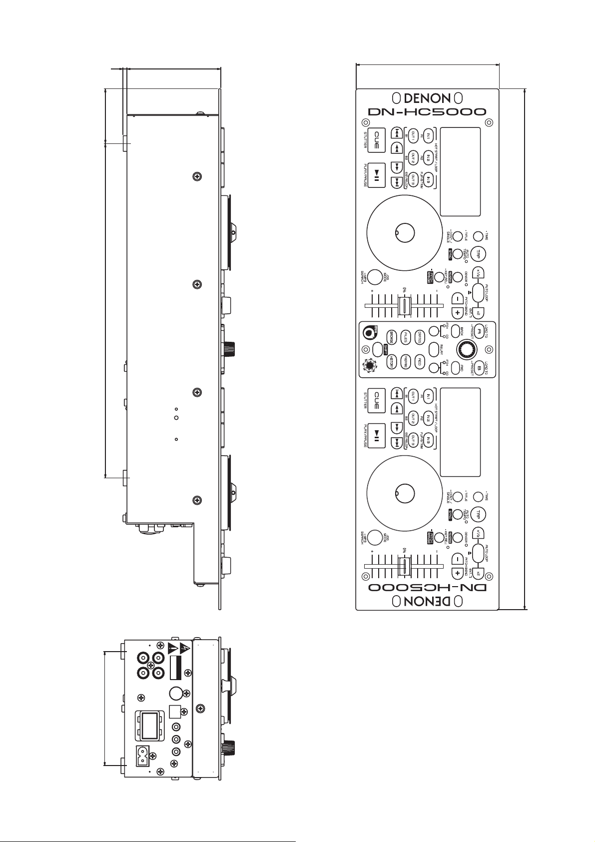
DIMENSION
-*/&065
-*/&065
0/0''
108&3
"$*/
-
3
䇭%&/0/
䇭%/%
䇭#6POMZ
㪩㪠㪪㪢㩷㪦㪝㩷㪜㪣㪜㪚㪫㪩㪠㪚㩷㪪㪟㪦㪚㪢
㪚㪘㪬㪫㪠㪦㪥
㪛㪦㩷㪥㪦㪫㩷㪦㪧㪜㪥
'PSVTFXJUI
%3*7&
64##
9$0/530-
'"%&3
'"%&3
3
Page 4
WIRE ARRANGEMENT
CX111
CX061
If wire bundles are untied or moved to perform adjustment or parts replacement etc., be sure to rearrange them neatly as
they were originally bundled or placed afterward.
Otherwise, incorrect arrangement can be a cause of noise
generation.
※Refer to 6~8 page for folding the FFC.
(1) The cord holder folds as shown on the diagram.
(2) Fasten the FFC to externals of figure with a cord holder.
(3) Fasten the 6P connector with a cord holder.
4
Page 5
(4) Fasten the two 4P connectors with a cord holder.
CX042
CX272
CX271
CX041
•Fasten the cord not to touch the trans.
(5) It coverd with TOP PANEL SUB ASSY.
NOTE:The wire gets caught in TOP PANEL SUB ASSY.
5
Page 6
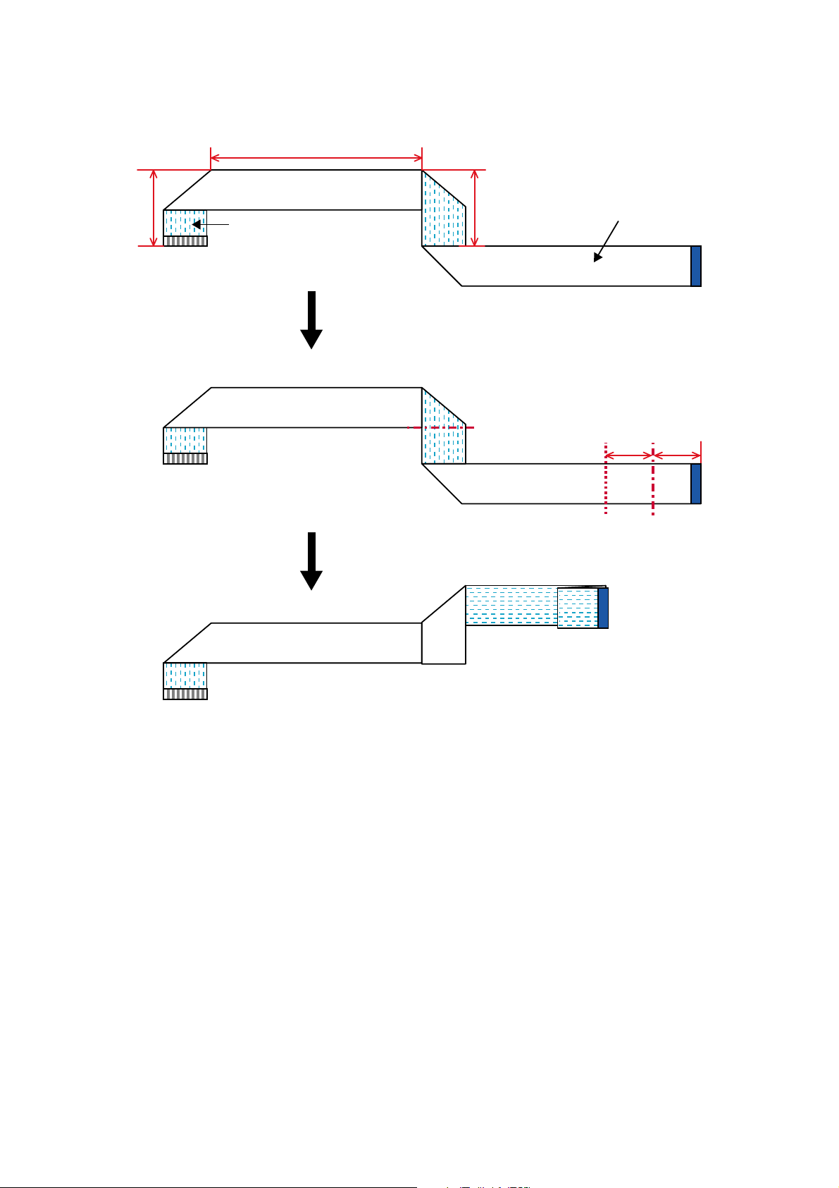
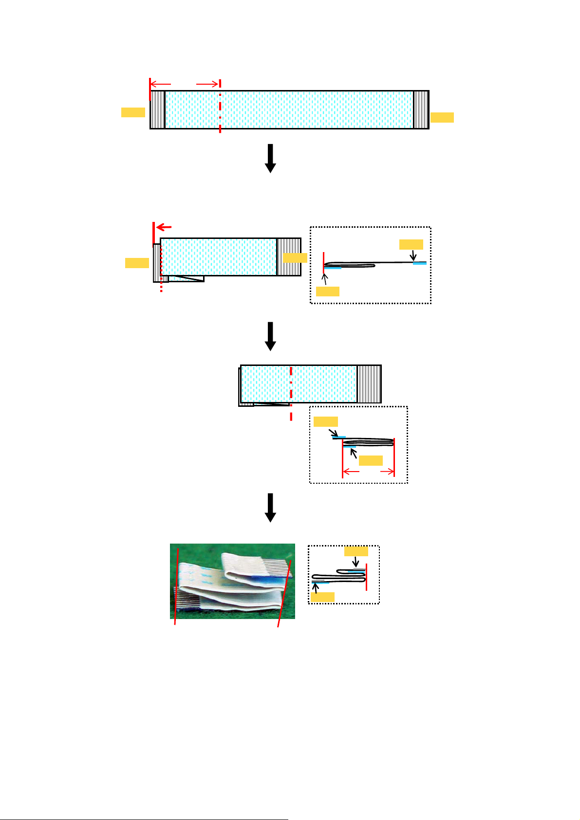
Folding the FFC
Printed surface
Fold as shown on the diagram.
45mm
160mm
55mm
White surface
35mm 35mm
Fold as shown on the diagram.
Fold inward
Fold inward
Fold outward
(1) 8U-110066-1 PANEL1 UNIT (00D0090290040 : 27P FFC(1.0) L=400)
6
Page 7
(2) 8U-110066-2 PANEL2 UNIT (00D0090290053 : 27P FFC(1.0) L=200 )
Fold inward
Fold inward
Fold outward
Fold outward
Fold outward
45mm
5mm
Fold as shown on the diagram.
Fold as shown on the diagram.
25mm
65mm
7
Page 8
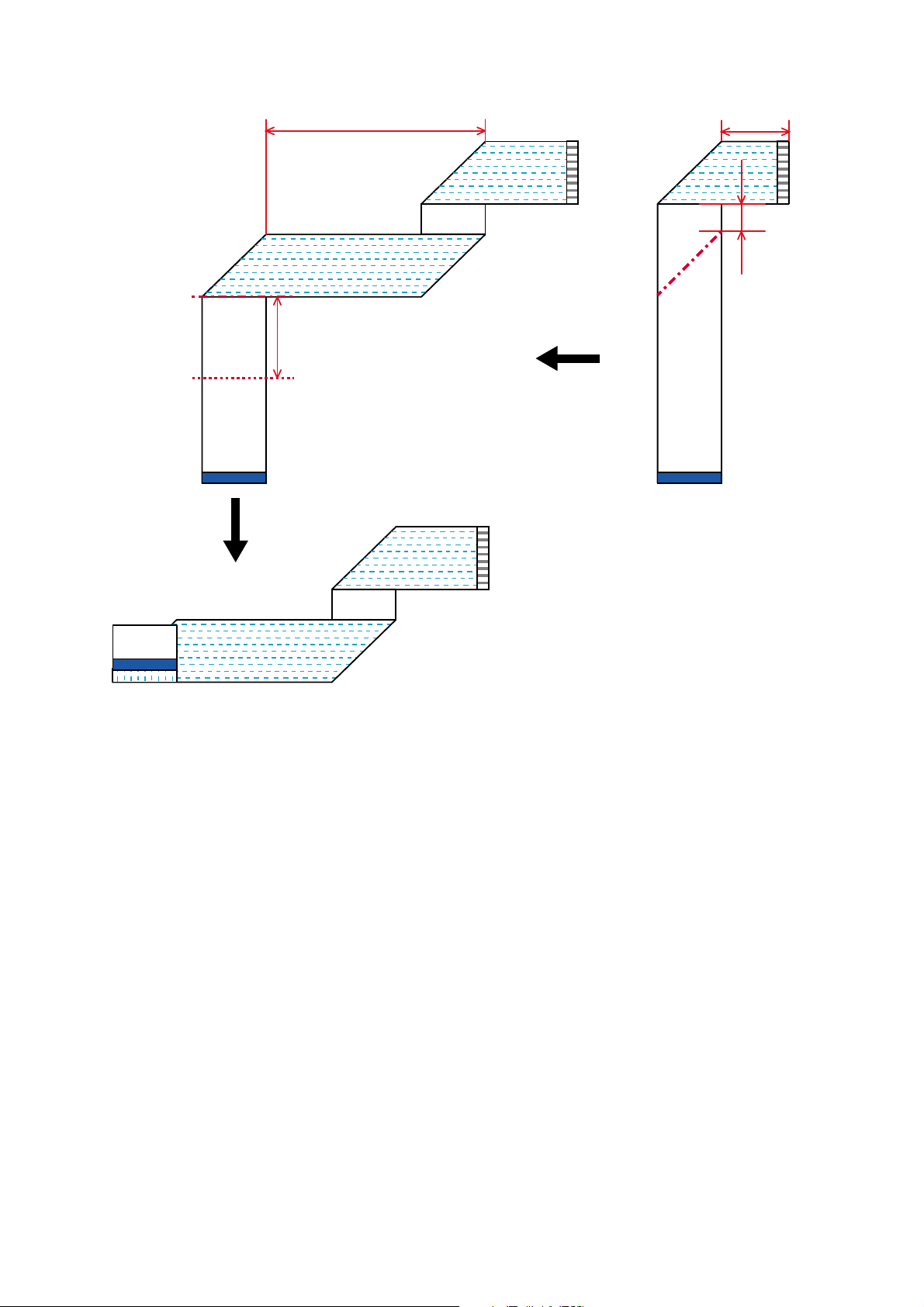
(3) 8U-110066-5 DISC1 UNIT / 8U-110066-6 DISC2 UNIT
㪘㩷㫊㫀㪻㪼
㪘㩷㫊㫀㪻㪼
㪘㩷㫊㫀㪻㪼
㪘㩷㫊㫀㪻㪼
16mm
㪘㩷㫊㫀㪻㪼
㪙㩷㫊㫀㪻㪼
㪙㩷㫊㫀㪻㪼
㪙㩷㫊㫀㪻㪼
㪙㩷㫊㫀㪻㪼
16mm
㪙㩷㫊㫀㪻㪼
Fold as shown on the diagram.
Fold inward
Fold inward
Fold outward
Place fold against the A side.
(00D0090290037 : 11P FFC(1.0) L=60)
8
Page 9
DISASSEMBLY
(Follow the procedure below in reverse order when
reassembling.)
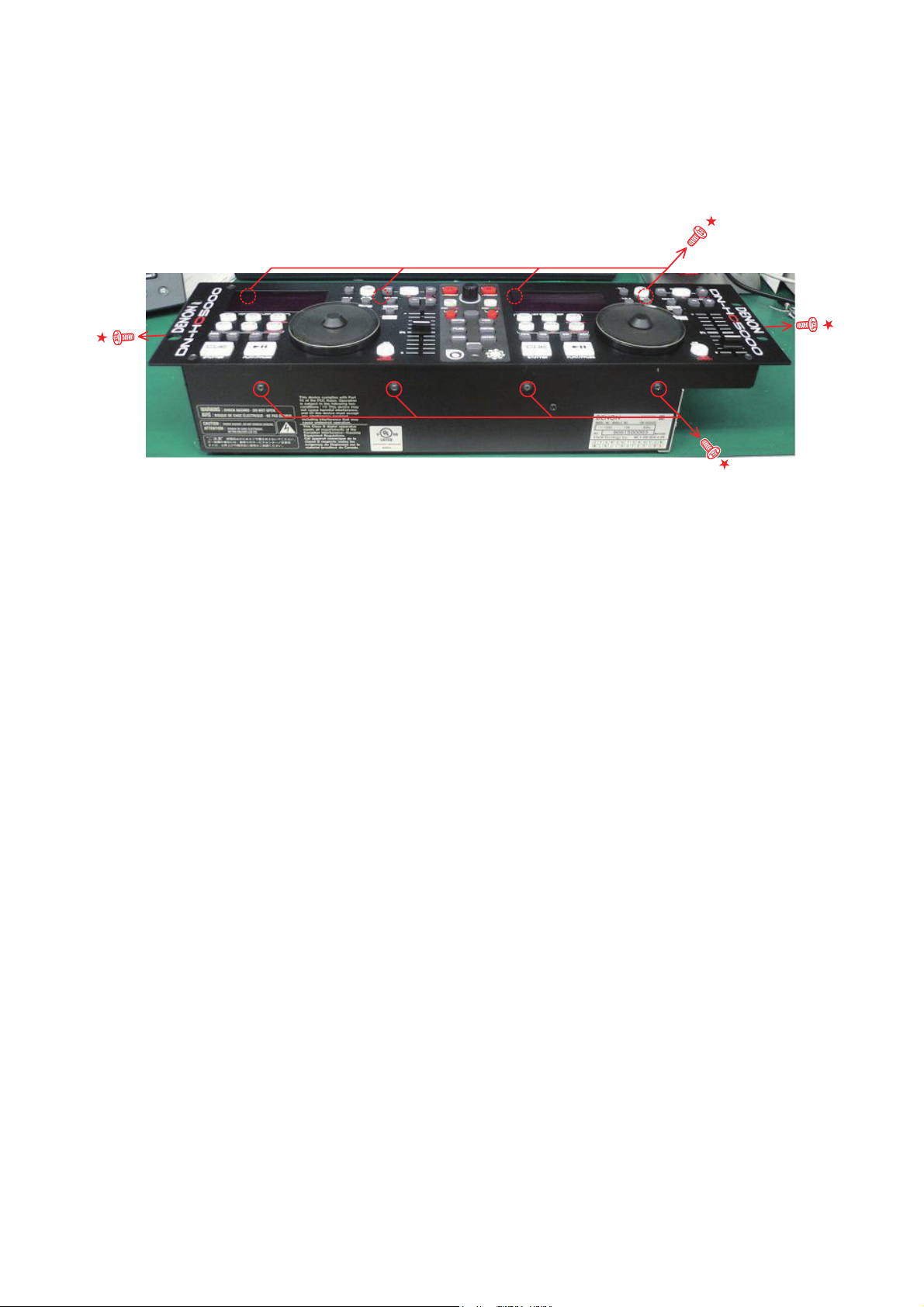
1. Top Panel Unit
(1) Remove 10 side screws with washer and pull up the Top Panel Unit.
Notes: Do not pull out aslant to prevent FFC cable damage.
Do not fail to pull AC cord from wall outlet before disconnect the FFC cable and wire.
If AC cord is remained plugged into wall outlet, power is kept supplied in the unit, which may cause damage.
9
Page 10
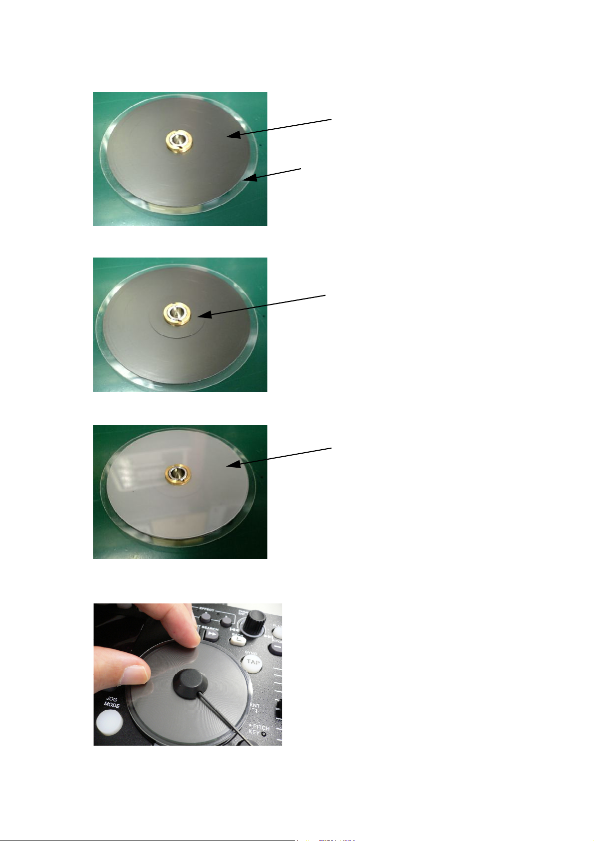
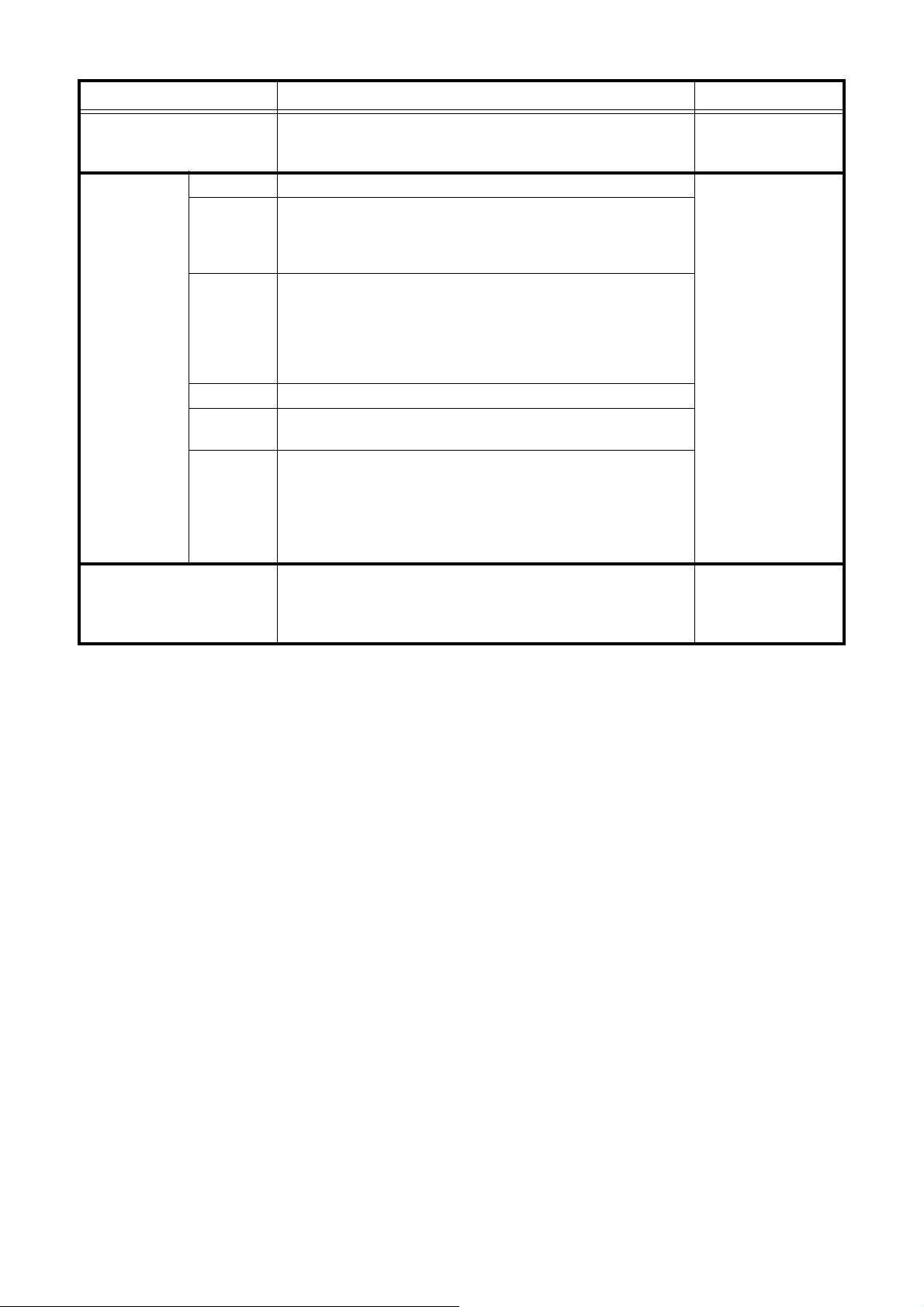
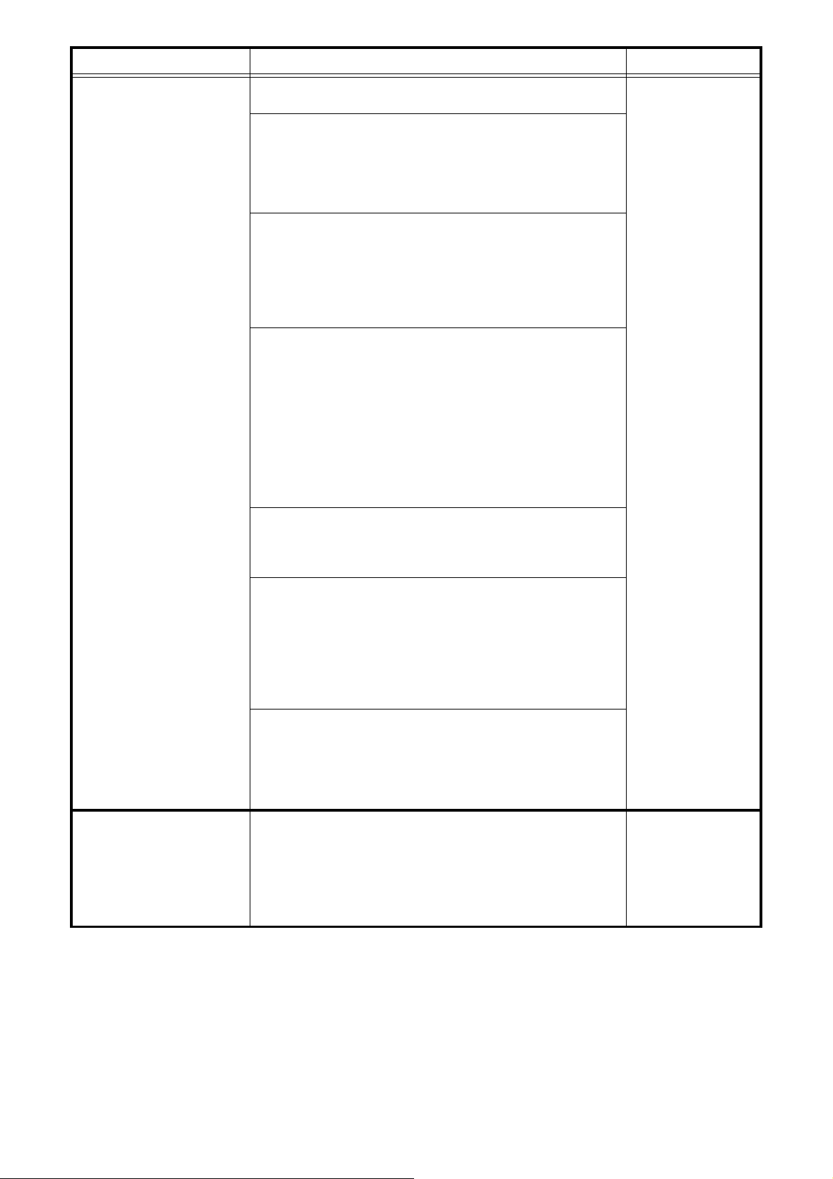
ASSEMBLY NOTE
Mounting the JOG DISC
(1) Mount SLIP MAT (B) on the JOG WHEEL SUB ASSY.
(2) Next mount SLIP MAT.
SLIP MAT (B) : Ref No. 34
(The slip mat has no specific front or rear side.)
JOG WHEEL SUB ASSY : Ref No. 38
SLIP MAT : Ref No. 35
(The slip mat has no specific front or rear side.)
(3) Next mount SLIP MAT.
SLIP MAT : Ref No. 36
(luster surface)
(4) Turn over, being careful that the piled slip mats do not fall, and set on the main unit. Hold the JOG WHEEL SAB ASSY,
then tighten the screw using a hexagonal wrench (2.6 x 3 BSS).
10
Page 11

SERVICE MODE
1. Turning on the power in the service mode
(1) Turn on the power while pressing the PARAMETERS knob and the NEXT button (Deck 1 or Deck 2) simultaneously.
The following appears on the VFD segment display section:
Service Mode
Function CHK
(2) When the PARAMETERS knob is turned clockwise, the display on the lower tier of the VFD segment display section
switches in the following order: "Function CHK" → "SW Check" → "Panel CHK" → "Touch MEAS".
The display switches in the opposite order when the PARAMETERS knob is turned counterclockwise.
(3) The displayed mode can be selected by pressing the PARAMETERS knob.
※ The service mode switches simultaneously for Deck 1 and Deck 2. When the operations for selecting and executing the
different check modes are performed for one deck, they are automatically performed for the other deck as well.
For some items, however, the selection and execution operation must be performed individually for Deck 1 and Deck 2.
(“SW CHECK”, “Panel CHK”, “Touch MEAS”)
2. Function summary
※ Refer to [3. Service mode function table] for details.
(1) Checking the operation of the function (Function CHK)
When the item to be checked is selected from the TOP menu, the device performs the check and settings and the results
are displayed on the VFD segment display section.
• Equipped function
① Setting initialization
② Drive Terminal check
③ Audio signal output
④ Audio Mute check
⑤ Touch initialization
⑥ USB-HIDI command transmission
(2) Checking the operation of the switches(SW Check)
Once all the switches on the panel surface have been pressed, the switch check mode ends automatically.
(3) Checking the operation of the panel(Panel CHK)
• Checking the operation of the various control elements on the panel surface
① PARAMETERS knob
② JOG disc
③ FADERIN
④ X-Control level
⑤ FADER level
• The functions shown below are always available while in the panel check mode.
⑥ All LEDs lit /LED DIM lit/All LEDs off
(4) Touch measurement(Touch MEAS)
Measurement of the count value when the touch sensor section is not being touched, and measurement and judgment
of the amount of change of the count value when the touch sensor section is being touched.
11
Page 12
3. Service mode function table
Mode Summary Remark
Service Mode TOP
(Service Mode)
Function
check mode
(Function CHK)
Switch check mode
(SW Check)
Turn on the power while pressing the PARAMETERS knob and the
NEXT button (Deck 1 or Deck 2) simultaneously.
→ Service mode starts
HC5000 Int, The various parameters are set to the factory defaults.
When executed with the drive terminal's Tx and Rx pins connected
Drive Check
Audio OUT
Mute Check Switches the hardware's muting circuit on and off.
Touch Init.
USB-HIDI
externally, the loop-back test is performed.
The device checks whether the transferred and received contents
are the same and the results are displayed.
The device's built-in 24 bit/44.1 kHz sampling frequency 1 kHz/0dB
audio signal is played.
Turn the PARAMETERS knob to select whether the output is on or
off, then press the PARAMETERS knob to execute.
During playback, the letters "OUT" on the VFD segment display
section flash.
Sets the contents of the EPROM built into the touch sensor IC to
the factory defaults.
Sends the HIDI/MIDI command corresponding to the function
selected on the VFD segment display section.
Turn the PARAMETERS knob clockwise to select the function in
the order shown below.
"CUE" → "PLAY" → "A1" → "A2" → "HOT1"
※ Refer to [3.3. MIDI Ccommands table] for details.
Initially, the VFD is all off, and when a switch is pressed, the corresponding VFD characters lit. → Once all the switches are pressed,
"Complete" is displayed on the VFD segment display section.
※ Refer to [3.1. Switch check mode] for details.
To cancel the service
mode, turn the power
off.
Press the BACK button
to return to the top
level of the Function
check mode.
Press the PARAMETERS knob to return to
the top level of the
Switch check mode.
12
Page 13
Mode Summary Remark
Panel check mode
(Panel CHK)
Touch measurement mode
(Touch MEAS)
※ Display of the status and results of the various control elements
on the panel surface and external input from the side panel
• PARAMETERS knob
The segment on the right side of the "P" column at the upper left
of the VFD segment display section toggles between white and
black each time the PARAMETERS knob is pressed.
When the PARAMETERS knob is turned, -> (clockwise) or <(counterclockwise) is displayed.
• JOG disc
When a touch is detected: The center of the scratch marker at
the bottom right of the VFD display section lights.
The left and right display sections of the scratch marker light
according to the direction of rotation.
The jog rev count detection result is displayed on the frame count
display section.
• PITCH slider
The pitch signal's AD conversion value is displayed on the pitch
display section.
The center tap value is displayed in three digits on the track number display section.
<Spec>
Central tap display value : CENTER = 512 ± 77
Pitch signal display value
• MAX value : 1018 or more
• Central click position : PITCH = CENTER ± 25
• MIN value : 6 or less
• FADERIN
The segment display sections at the sides of FC and FP on the
VFD segment display section are displayed as ■ while the CUE
and PLAY fade-in signals are being detected, respectively.
• X-Control
The AD conversion values of the X-Fade and CH signals are displayed at the sides of XF and XC on the VFD segment display
section.
• XF display value
• MAX value : 1010 or more
• MIN value : 10 or less
• XC display value : 0 fixation → Future
• LED/VFD light/off
When the TAP button is pressed, the display toggles in the fol-
lowing order: All LEDs lit + VFD all lit → LED DIM lit + VFD off →
LED off + normal VFD display
※This function is always available while in the "Panel CHK"
mode.
The count value detected by the touch sensor IC is displayed on
the VFD.
OK if the difference between the count value when not being
touched and the count value when touched is 50 or greater.
OK if the count value when not being touched is between the
range of 100 and 300.
※ Refer to [3.2. Touch measurement mode] for details.
Press the BACK button
to return to the top
level of the panel
check mode.
Press the BACK button
to return to the top
level of the Touch measurement mode.
13
Page 14
3.1. Switch check mode (SW Check)
AC
PPHFC
CAFL+ B BR
S
-
(1) All the VFD characters are turned off.
The following characters are assigned to the 12 places of the VFD segment display section:
(2) When each switch is pushed
IN1 → Turn on the pertinent figure in the third place of the track number.
IN2 → Turn on the pertinent figure in the second place of the track number.
IN3 → Turn on the pertinent figure in the first place of the track number.
OUT1 → Turn on the second place of the minutes display counter.
OUT2 → Turn on the first place of the minutes display counter.
OUT3 → Turn on the second place of the seconds display counter.
AUTO TEMPO → Turn on the "A" in the first place of first row.
PITCH BEND- → Turn on the "-" in the fourth place of first row.
PITCH BEND+ → Turn on the "+" in the fifth place of first row.
TIME → Turn on the "REMAIN" .
TITLE → Turn on the "CONT".
AUTO LOOP → Turn on the "CD".
8 → Turn on the " ( " of A1.
9 → Turn on the " ) " of A1.
6 → Turn on the " ( " of A2.
7 → Turn on the " ) " of A2.
JOG MODE → Turn on the "MP3".
KEY ADJ → Turn on the "KEY ADJ".
TAP → Turn on the "BPM".
1/2 → Turn on the second place of BPM.
*2 → Turn on the first place of BPM.
ITCH/CD → Turn on the "PC".
CENSOR → Turn on the "C" in the second place of first row.
LOAD A/B → Turn on the "L" in the third place of first row.
BACK → Turn on the "B" in the eighth place of first row. (DECK 1,2 is displayed simultaneously)
CRATES → Turn on the "C" in the ninth place of first row. (DECK 1,2 is displayed simultaneously)
FILES → Turn on the "F" in the tenth place of first row. (DECK 1,2 is displayed simultaneously)
BROWSE → Turn on the "B" in the eleventh place of first row. (DECK 1,2 is displayed simultaneously)
RELAY → Turn on the "R" in the twelfth place of first row. (DECK 1,2 is displayed simultaneously)
CUE → Turn on the "C" in the first place of second row.
PLAY →
FWD → Turn on the "F" in the seventh place of second row. (DECK 1,2 is displayed simultaneously)
ADD → Turn on the "A" in the ninth place of second row. (DECK 1,2 is displayed simultaneously)
PREPARE → Turn on the "P" in the tenth place of second row. (DECK 1,2 is displayed simultaneously)
HISTORY → Turn on the "H" in the eleventh place of second row. (DECK 1,2 is displayed simultaneously)
SHIFT → Turn on the "S" in the twelfth place of second row. (DECK 1,2 is displayed simultaneously)
Turn on the "P" in the second place of second row.
(3) Once all the switches have been pressed, "Complete" is displayed on the second row of the VFD segment display
section.(both decks)
For both decks, press any switch while "Complete" is displayed to return to the top level of the switch check mode.
14
Page 15

3.2. Touch measurement mode(Touch MEAS)
(1) All the VFD characters are turned off.
The following appears on the VFD segment display section:(Count value display mode)
TP_***RT_***
BM_***LT_***
*** : Current touch count value is displayed.
(TP : TOP, BM : BOTTOM, RT : RIGHT, LT : LEFT)
The average of the count values acquired for the first four times measurements are made after this mode is set is
calculated and used as the reference value.
(2) Turn the PARAMETERS knob one click to switch the display on the VFD segment display section as shown below.
(Difference display mode)
TP
BM
*** : (Standard value) - (Current touch count value) is displayed.
Now, turn the PARAMETERS knob one click to switch to the count display mode in (1).
(3) The center of the scratch mark lights if the difference of the count value calculated with any one of the four sensors
above, below and to the sides of the disc during the touch measurement mode is 50 or greater.
(4) When the PARAMETERS knob is pressed, the average of the count value acquired for the first four times measure-
ments are made after the PARAMETERS knob is pressed is held on the display.
(5) Press the PARAMETERS knob again to return to the count display mode in (1).
(6) Press the BACK and PLAYLIST buttons to return to the top level of the Touch measurement mode.
***RT
▲
***LT
▲
***
▲
***
▲
15
Page 16

3.3. MIDI COMMANDS
(1) Data transmission
The panel operation data is transmitted by MIDI command, as per the table below.
● Send command to PC
items
1Playlist
2 JOG mode
3 Pitch/KEY
4TAP
5 Pitch Bend+
6 Pitch Bend-
7 Fast search+
8 Fast search-
9EFX1/ECHO/LOOP
10 EFX2/FLANGER
11 EFX3/FILTER
12 HOT1
13 HOT2
14 HOT3
15 HOT4
16 HOT5
17 TIME/TOTAL
18 MEMO/PRESET
19 TITLE
20 CONT./SINGLE
21 Parameters KNOB SW
22 BACK
23 SOURCE mode
24 FLIP
25 A1
26 A2
27 B
28 EXIT/Reloop
29 Cue
30 Play
31 JOG UP
32 JOG DOWN
33 JOG LEFT
34 JOG RIGHT
35 Jogwheel touch
36 Preset Mode
37 D4500 Cont. mode
38 Jogwheel fwd/rev 0xBn 0x51
Command Number Value
SW ON : 0x9n
SW OFF : 0x8n
↑
↑
↑
↑
↑
↑
↑
↑
↑
↑
↑
↑
↑
↑
↑
↑
↑
↑
↑
↑
↑
↑
↑
↑
↑
↑
↑
↑
↑
↑
↑
↑
↑
↑
SW ON : 0x9n
SW OFF : 0x8n
↑
MIDI command
0x02
0x04
0x05
0x07
0x08
0x09
0x10
0x11
0x12
0x13
0x14
0x17
0x18
0x19
0x20
0x21
0x23
0x24
0x25
0x26
0x28
0x30
0x31
0x36
0x37
0x38
0x39
0x40
0x42
0x43
0x47
0x48
0x49
0x50
0x51
0x52
0x53
SW ON : 0x40
SW OFF : 0x00
↑↑
↑↑
↑↑
↑↑
↑↑
↑↑
↑↑
↑↑
↑↑
↑↑
↑↑
↑↑
↑↑
↑↑
↑↑
↑↑
↑↑
↑↑
↑↑
↑↑
↑↑
↑↑
↑↑
↑↑
↑↑
↑↑
↑↑
↑↑
↑↑
↑↑
↑↑
↑↑
↑↑
↑↑
SW ON : 0x40
SW OFF : 0x00
↑↑
Reverse 0x3F ~ 0x01
Foward 0x41 ~ 0x7F
slow
→ fast
Message type
Note ON/OFF
Note ON/OFF
Control change
※ relative data
39 X-Control fader
Parameters KNOB
40
Increment/Decrement
41 Pitch Slider 0xEn 0xllh (LSB) 0xmmh (MSB) Pitch bend change
↑
↑
0x53
0x54
-100% : 0x7F7F (MSB/LSB)
0% : 0x4000 (MSB/LSB)
+100% : 0x0000 (MSB/LSB)
0x00 (min) → 0x7F
(max)
"Increment : 0x00
Decrement : 0x7F"
↑
↑
n = MIDI CH
16
Page 17

(2) Data reception
LED data reception
The panel operation data is transmitted by MIDI command, as per the table below.
● Receive command for LED
items
LED 0xBn
1 Playlist 0x02
2 Pitch match LED 0x04
3 JOG mode Green 0x05
4 JOG mode Orange 0x06
5 Pitch/KEY Green 0x07
6 Pitch/KEY Orange 0x08
7 TAP Green 0x09
8 TAP Orange 0x0A
9 EFX1/ECHO/LOOP RED 0x0B
10 EFX1 Green 0x0C
11 EFX2/FLANGER RED 0x0D
12 EFX2 Green 0x0E
13 EFX3/FILTER RED 0x0F
14 EFX3 Green 0x10
15 HOT1 0x11
16 HOT1 Dimmer 0x12
17 HOT2 0x13
18 HOT2 Dimmer 0x14
19 HOT3 0x15
20 HOT3 Dimmer 0x16
21 HOT4 0x17
22 HOT4 Dimmer 0x18
23 HOT5 0x19
24 HOT5 Dimmer 0x1A
25 Parameter KNOB 0x1E
26 A1 0x24
27 A1 Dimmer 0x3C
28 A2 0x25
29 A2 Dimmer 0x3D
30 Cue 0x26
31 Play 0x27
32 Jogwheel 0x3B
33 Pitch slider request
34 X-Control fader request
Command Number Value
MIDI command
ON TRG : 0x4A
OFF TRG : 0x4B
Blink ON TRG : 0x4C
only Use 0x4A
(request TRG)
only Use 0x4A
(request TRG)
↓
0x3C
0x3D
Message type Notes
Control Change
DN-HC5000 return
pitch slider position
DN-HC5000 return
XControl fader position
n = MIDI CH
17
Page 18

VFD symbol data reception
The Various Vfd Symbols Can Be Set To On, Off Or Blinking, As Per The Table Below.
● Receive command for VFD Symbol
items
Command Number Value
VFD Symbol 0xBn
1T.
2 REMAIN
3 ELAPSED
4CONT.
5SINGLE
6 BPM
7m
8s
9f
10 Pitch dot Right
11 Pitch dot center
12 Pitch dot left
13 MP3
14 WAV
15 KB
16 KEY ADJ.
17 MEMO
18 ( : A1 side
19 ( : A2 side
20 ) : A1 side
21 ) : A2 side
22 A1
23 A2
24 B : A1 side
25 B : A2 side
26 Scratch Ring out side
27 Scratch Ring in side
28 Touch dot
29 Track Position Blink only Use 0x4F/0x4E
30 Scratch Position 1 (Top right) only Use 0x4D/0x4E
31 Scratch Position 2 only Use 0x4D/0x4E
32 Scratch Position 3 only Use 0x4D/0x4E
33 Scratch Position 4 only Use 0x4D/0x4E
34 Scratch Position 5 only Use 0x4D/0x4E
35 Scratch Position 6 only Use 0x4D/0x4E
36 Scratch Position 7 only Use 0x4D/0x4E
37 Scratch Position 8 only Use 0x4D/0x4E
38 Scratch Position 9 only Use 0x4D/0x4E
39 Scratch Position 10 only Use 0x4D/0x4E
MIDI command
ON TRG : 0x4D
OFF TRG : 0x4E
Blink ON TRG : 0x4F
↓
0x01
0x02
0x03
0x04
0x05
0x06
0x07
0x08
0x09
0x0A
0x0B
0x0C
0x10
0x11
0x13
0x14
0x15
0x16
0x17
0x18
0x19
0x1A
0x1B
0x1C
0x1D
0x1E
0x1F
0x20
0x21
0x22
0x23
0x24
0x25
0x26
0x27
0x28
0x29
0x2A
0x2B
Message type
Control Change
18
Page 19
items
VFD Symbol 0xBn
40 Scratch Position 11 only Use 0x4D/0x4E
41 Scratch Position 12 only Use 0x4D/0x4E
42 Scratch Position 13 only Use 0x4D/0x4E
43 Scratch Position 14 only Use 0x4D/0x4E
44 Scratch Position 15 only Use 0x4D/0x4E
45 Scratch Position 16 (Bottom) only Use 0x4D/0x4E
46 Scratch Position 17 only Use 0x4D/0x4E
47 Scratch Position 18 only Use 0x4D/0x4E
48 Scratch Position 19 only Use 0x4D/0x4E
49 Scratch Position 20 only Use 0x4D/0x4E
50 Scratch Position 21 only Use 0x4D/0x4E
51 Scratch Position 22 only Use 0x4D/0x4E
52 Scratch Position 23 only Use 0x4D/0x4E
53 Scratch Position 24 only Use 0x4D/0x4E
54 Scratch Position 25 only Use 0x4D/0x4E
55 Scratch Position 26 only Use 0x4D/0x4E
56 Scratch Position 27 only Use 0x4D/0x4E
57 Scratch Position 28 only Use 0x4D/0x4E
58 Scratch Position 29 only Use 0x4D/0x4E
59 Scratch Position 30 only Use 0x4D/0x4E
60 Scratch Position 31 only Use 0x4D/0x4E
61 Scratch Position 32 (Top) only Use 0x4D/0x4E
Command Number Value
MIDI command
ON TRG : 0x4D
OFF TRG : 0x4E
Blink ON TRG : 0x4F
↓
0x2C
0x2D
0x2E
0x2F
0x30
0x31
0x32
0x33
0x34
0x35
0x36
0x37
0x38
0x39
0x3A
0x3B
0x3C
0x3D
0x3E
0x3F
0x40
0x41
Message type
Control Change
n = MIDI CH
※ Track Position Blink” sets blinking of the entire track position display segment on or off.
19
Page 20

VFD parameter data reception
The time-related display and segment display can be set by MIDI command, as per the table below.
● Receive command for VFD Parameter
Items
VFD Parameter
1 Tr number MSB 0xBn 0x40
2 Tr number LSB
3 Time mini
4Time sec
5 Time frame
6Pitch POL
7Pitch MSB
8Pitch LSB
9 Track Position
10 Segment 1-1 MSB
11 Segment 1-2 MSB
12 Segment 1-3 MSB
13 Segment 1-4 MSB
14 Segment 1-5 MSB
15 Segment 1-6 MSB
16 Segment 1-7 MSB
17 Segment 1-8 MSB
18 Segment 1-9 MSB
19 Segment 1-10 MSB
20 Segment 1-11 MSB
21 Segment 1-12 MSB
22 Segment 1-1 LSB
23 Segment 1-2 LSB
24 Segment 1-3 LSB
25 Segment 1-4 LSB
26 Segment 1-5 LSB
27 Segment 1-6 LSB
28 Segment 1-7 LSB
29 Segment 1-8 LSB
30 Segment 1-9 LSB
31 Segment 1-10 LSB
32 Segment 1-11 LSB
33 Segment 1-12 LSB 0xBn 0x2D 0x00 ~ 0x0F Control Change
34 Segment 2-1 MSB
35 Segment 2-2 MSB
36 Segment 2-3 MSB
37 Segment 2-4 MSB
Command Number Value
↑
↑
↑
↑
↑
↑
↑
↑
↑
↑
↑
↑
↑
↑
↑
↑
↑
↑
↑
↑
↑
↑
↑
↑
↑
↑
↑
↑
↑
↑
↑
↑↑
↑↑
↑↑
↑↑
MIDI command
100-109 : “-0” to”-9”
110 : “-”, 111 : “ "
0x41
0x42
0x43
0x44
0x45
0x46
0x47
0x48 normal
0x49 reverse
0x01 0x00 ~ 0x0F
0x02
0x03
0x04
0x05
0x07
0x08
0x09
0x0A
0x0B
0x0C
0x0D
0x21
0x22
0x23
0x24
0x25
0x27
0x28
0x29
0x2A
0x2B
0x2C
Message Type
0-99
Control Change
↑↑
↑↑
↑↑
↑↑
" “ 0x00
“+” 0x01
“-” 0x02"
↑
↑↑
↑↑
0-100%
↑
↑
↑↑
↑↑
↑↑
↑↑
↑↑
↑↑
↑↑
↑↑
↑↑
↑↑
↑↑
↑↑
↑↑
↑↑
↑↑
↑↑
↑↑
↑↑
↑↑
↑↑
↑↑
↑↑
0x0E
0x0F
0x10
0x11
↑
↑
↑
↑
20
Page 21

38 Segment 2-5 MSB
39 Segment 2-6 MSB
40 Segment 2-7 MSB
41 Segment 2-8 MSB
42 Segment 2-9 MSB
43 Segment 2-10 MSB
44 Segment 2-11 MSB
45 Segment 2-12 MSB
46 Segment 2-1 LSB
47 Segment 2-2 LSB
48 Segment 2-3 LSB
49 Segment 2-4 LSB
50 Segment 2-5 LSB
51 Segment 2-6 LSB
52 Segment 2-7 LSB
53 Segment 2-8 LSB
54 Segment 2-9 LSB
55 Segment 2-10 LSB
56 Segment 2-11 LSB
57 Segment 2-12 LSB
n = MIDI CH
↑↑
↑↑
↑↑
↑↑
↑↑
↑↑
↑↑
↑↑
↑↑
↑↑
↑↑
↑↑
↑↑
↑↑
↑↑
↑↑
↑↑
↑↑
↑↑
↑↑
0x12
0x13
0x14
0x15
0x16
0x17
0x18
0x19
0x2E
0x2F
0x30
0x31
0x32
0x33
0x34
0x35
0x36
0x37
0x38
0x39
↑
↑
↑
↑
↑
↑
↑
↑
↑
↑
↑
↑
↑
↑
↑
↑
↑
↑
↑
↑
21
Page 22

VFD segment data reception
The various segments are set by 2-byte data, as per the following font code.
(0x00/0x00 to 0x00/0x07 cannot be used.)
● Font codes for segments
※ For the Reflex function operations corresponding to the above MIDI commands, refer to the Reflex manual.
22
Page 23

CAUTION IN SERVICING
When replacing the MAIN P.W.B. UNIT
When replacing the MAIN P.W.B. UNIT, be sure to perform update to latest firmware after replacement.
VERSION UPGRADE PROCEDURE OF FIRMWARE
※ When replacing the MAIN P.W.B. UNIT, how to enter version up modes is different.
Refer to 1.2.procedure [When replacing the MAIN P.W.B.] (1).
1.1. preparation
(1) Connect the computer by USB cable.
1.2. procedure
※ Turn on the device’s power in the update mode.
(1) Turn on the power while pressing the OUT3 and BACK buttons simultaneously on Deck1 or Deck2.
[When replacing the MAIN P.W.B.]
(1) Turn on the power while pressing the PARAMETERS knob and the OUT3 button (Deck 1 or Deck 2) simultaneously.
The following appears on the VFD segment display section:
Update Mode
Ver****
on Deck1
The version informationis displayed.
PC Linked
Don t Touch!
on Deck2
If the device is not yet connected, the following appears on the VFD segment display section:
PC Disconn..
on Deck2
(2) Launch the DN-HC5000 update program.
The screen shown below appears on thecomputer.
Current version information
The identified device name is displayed.
23
Page 24

(3) If the device is not connected or not in the update mode at this time, the screen shown below is displayed.
If the update file has not been loaded, “Fileis not ready.” is displayed.
The device is not in the update mode.
(4) Drag and drop the update file to the ”DENON DJ Upgrade program” screen.
The Load button can now be selected.
24
Page 25

(5) Press the Load button to transfer the update file.
(6) The following appears on the VFD segment display section:
During file transfer:on Deck1
Update Mode
Loading
Once file transfer is finished;
Update Mode
**** >> ****
(Left side: Old version, Right side: New version)
Once file transfer is finished, press the OK button. The Execute button is now enabled (can be pressed).
25
Page 26

(7) Press the Execute button to begin updating the version.
Once version updating is completed, “Version up was completed.” is displayed.
The following appears on the VFD segment display section during version updating:
On Deck1:
Update Mode
Updating
Once version updating is completed:
Update Mode
Completed
If version updating has failed, “Version up was not completed.” is displayed and the screen returns to as it was before
the Execute button was pressed. Press the Execute button again.
(8) Press the OK button to finish.
The following appears on the VFD segment display section:
On Deck2:
PC Linked
Power Off!!
Quit the updating program and turn off the DN-HC5000’s power.
26
Page 27

NOTE:
• Do not turn off the set’s power or disconnect the cable connecting it to the computer during loading or version updating.
Also, do not press any buttons on the set or any keys on the computer’s keyboard.
• If an error message appears during loading or version updating, repeat from step 1.
Other error messages are as follows:
“File is invalid”
When the loaded update file was invalid.
“Load failed. Check the connection, and retry”
When a transfer error has occurred during transfer of the update file to the device.
“Loaded data is invalid. Check the file.”
When a SUM check error has occurred after transfer of the update file to the device.
“Version up was not completed.”
When version updating was not completed normally.
27
Page 28

TROUBLE SHOOTING
FLOW CHART NO.1
The power cannot be turned on.
Is the fuse normal?
Yes
Is normal state restored when once unplugged
power cord is plugged again after several seconds?
Yes
Is the +5VD line voltage normal?
Yes
Check each rectifying circuit of the secondary circuit
and replace it if defective.
FLOW CHART NO.2
The fuse blows out.
Check the presence that the primary component
is leaking or shorted and replace it if defective.
After servicing, replace the fuse.
FLOW CHART NO.3
+5VD is not outputted.
Is the voltage of 9V or more supplied to 1pin(Vcc)
of IC901?
Yes
Check IC901, D910, L902 and the periphery circuit,
and replace it if defective.
No
No
No
No
See FLOW CHART No.2 <The fuse blows out.>
Check if there is any leak or short-circuiting on the
primary circuit component, and replace it if defective.
(C903, C912, C913, C914, L901, BR901, T901)
Check the presence that the rectifying diode or
circuit is shorted in each rectifying circuit of
secondary side, and replace it if defective.
Check D914~D917 and the periphery circuit,
and replace it if defective.
FLOW CHART NO.4
+3.3V is not outputted.
Is 5V voltage supplied to 2pin(IN) of IC902?
Yes
Check IC902 and the periphery circuit,
and replace it if defective.
FLOW CHART NO.5
+1.2V is not outputted.
Is 5V voltage supplied to 2pin(Vcc) of IC401?
Yes
Check IC402 and the periphery circuit,
and replace it if defective.
FLOW CHART NO.6
+8V is not outputted.
Is the voltage of 10V or more supplied to
INPUTpin of IC904?
Yes
Check IC904 and the periphery circuit,
and replace it if defective.
No
No
No
Refer to FLOW CHART NO.3 [+5VD is not outputted.]
Check FB401, CX601 and the periphery circuit,
and replace it if defective.
Check D907, D908 and the periphery circuit,
and replace it if defective.
28
Page 29

FLOW CHART NO.7
-8V is not outputted.
Is the voltage of -10V or less supplied to INPUTpin
of IC905?
Yes
Check IC905 and the periphery circuit,
and replace it if defective.
FLOW CHART NO.8
+5VA is not outputted.
Is 8V voltage supplied to INPUTpin of IC801?
Yes
Check IC801 and the periphery circuit,
and replace it if defective.
FLOW CHART NO.9
HV is not outputted.
Is the voltage of 30V or more supplied to
collector terminalof TR904?
Yes
Check TR904 and the periphery circuit,
and replace it if defective.
FLOW CHART NO.10
F1/F2 is not outputted.
No
No
No
Check D903, D904 and the periphery circuit,
and replace it if defective.
Refer to FLOW CHART NO.6 [+8V is not outputted.]
Check D901, D902, D509, D906 and the
periphery circuit, and replace it if defective.
Is the regulated voltage(±15%) supplied to T901?
Yes
Is the regulated voltage(AC2.7V~AC3.3V) supplied
for T901?
Yes
Check if there is any leak or short-circuiting on the
primary circuit component, and replace it if defective.
FLOW CHART NO.11
The fluorescent display tube(FL701, FL801)
does not light up.
Is 3.3V voltage supplied to 36pins(VDD)
of FL701(FL801)?
Yes
Is 34V voltage supplied to 37pins(HV)
of FL701(FL801)?
Yes
Are the filament voltage supplied between 1, 2, 3pins
and 42, 43, 44pins of the fluorescent display tube
(FL701, FL801)? And the +5V voltage applied between
these pins and GND?
Yes
Replace the fluorescent display tube(FL701, FL801).
No
No
No
No
No
Refer to FLOW CHART NO.1
[The power cannot be turned on.]
Check T901, ZD903 and the periphery circuit,
and replace it if defective.
Check the +3.3V line and service it if defective.
Check the HV(+34V) line and service it if defective.
Check the F1/F2 line and service it if defective.
29
Page 30

FLOW CHART NO.12
The key operation is not functioning.
Are the contact point and the installation state of the
key switches (S701~734, S801~830) normal?
Yes
Does LED(LD701~739, LD801~829) light correctly ?
Yes
When pressing each switches, do the voltage of
each pin of IC702(IC802) (shown below) increase?
S704,709,713,715,719,702,730 : IC702 14pin
S717,721,725,727,718,729,701,706 : IC702 3pin
S703,708,712,716,731,724,733,726 : IC702 4pin
S707,711,734,720 : IC702 5pin
S710,714,723,722,728 : IC702 6pin
S802,806,810,812,816,820 : IC802 13pin
S823,824,825,815,817 : IC802 14pin
S821,826,827,828,819 : IC802 3pin
S801,805,809,811,829 : IC802 4pin
S803,807,830,813 : IC802 5pin
S804,808,818,814,822 : IC802 6pin
Yes
Replace IC702(IC802).
FLOW CHART NO.13
Both functions of picture and sound do not operate normally.
Start the service mode, and with both Deck the mode
of Function CHK→Audio OUT→1kHz All L&R is
sequentially selected.
Are the audio signals outputted to 14pin(Rch) and
15pin(Lch) of IC802(Deck1)and IC803(Deck2)?
Yes
Are the audio signals outputted to 7pin(Lch) and
1pin(Rch) of IC804(Deck1)and IC805(Deck2)?
Yes
Is 11pin of CY111 (MUTE control signal)H, and has
been the TR803 collector (MUTE drive signal) L(-8V)?
Yes
No
No
No
No
No
No
Check periphery circuit from 7pin and 1pin to
replace
JK801 of IC804 and IC805, and
it if
defective.
Re-install the switches (S701~734, S801~830)
correctly or replace the poor switch.
Check the TR701~708(TR807~814)and
their periphery, and service it if detective.
Check the switches (S701~734, S801~830) and
their periphery, and service it if detective.
Check the input signal from CY111 to IC802, IC803
and their periphery, and service it if detective.When the
input signal is correct, IC802 or IC803 is replaced.
Check periphery circuit from 14pin and 15pin to
IC804 and IC805 of IC802 and IC803, and service
it if defective. When the periphery circuit is correct,
IC804 or IC805 is replaced.
Check TR803 and the periphery circuit, and service it if
defective.
30
Page 31

LEVEL DIAGRAM
-10
-20
-30
-40
-50
-60
+6
OUTPUT
PC
CPU
SH7263
Audio
DAC
PCM178
LPF
+6.0dBV
0
0dBFS
GAIN=2.78dB
+2.78dBV
GAIN=3.22dB
16bit:SNR=98dB
24bit:SNR=106dB
-70
-80
-90
-100
-120
-130
-140
-150
16bit:SNR=98dB
㪉㪋㪹㫀㫋㪑㪪㪥㪩㪔㪈㪋㪍㪻㪙
PCM1781:SNR=106dB(typ)
-92dBV
-95.22dBV
-100dBV
-103.22dBV
31
Page 32

SEMICONDUCTORS
Only major semiconductors are shown, general semiconductors etc. are omitted to list.
1. IC’s
R5S72630P200FP (IC104)
.
32
Page 33

R5S72630P200FP Block Diagram
33
Page 34

R5S72630P200FP Terminal Function
Pin No. Pin Name Symbol I/O Function
1 PC10/-RASU /MUTE O General-purpose port Not used: OPEN
2 -CASL SHCAS O %CASL% SDRAM /CAS
3 -RASL SHRAS O %RASL% SDRAM /RAS
4 VCC V1SH Power supply for in Digital +1.2V
5 DQMUU - O DQMUU Not used: OPEN
6 VSS DGND Digital GND
7 PVSS DGND GND for I/O Digital GND
8 DQMUL - O DQMUL Not used: OPEN
9 PVCC V3SH Power supply for I/O
10 DQMLU DQMLU O DQMLU SDRAM DQMU
11 -CS0 CS0 O CS0 :FLASH ROM FLASH /E
12 -RD SHRD O %RD% FLASH /G
13 DQMLL DQMLL O DQMLL SDRAM DQML
14 PC3/-CS3 CS3 O CS3 SDRAM /CS
15 PC2/-CS2 - O General-purpose port Not used: OPEN
16 VCC V1SH Power supply for in Digital +1.2V
17 PC0/A0/-CS7 - O General-purpose port Not used: OPEN
18 VSS DGND Digital GND
19 PVSS DGND GND for I/O Digital GND
20 PC1/A1 SHA1 O A1 SDRAM/FLASH A0
21 PVCC V3SH Power supply for I/O Digital +3.3V
22 A2 SHA2 O A2 Same A1
23 A3 SHA3 O A3 Same A2
24 A4 SHA4 O A4 Same A3
25 A5 SHA5 O A5 Same A4
26 A6 SHA6 O A6 Same A5
27 A7 SHA7 O A7 Same A6
28 A8 SHA8 O A8 Same A7
29 PVCC V3SH Power supply for I/O Digital +3.3V
30 A9 SHA9 O A9 Same A8
31 PVSS DGND GND for I/O Digital GND
32 VSS DGND Digital GND
33 A10 SHA10 O A10 Same A9
34 VCC V1SH Power supply for in Digital +1.2V
35 A11 SHA11 O A11 Same A10
36 A12 SHA12 O A12 Same A11
37 A13 SHA13 O A13 FLASH A12
38 A14 SHA14 O A14 FLASH A13
39 A15 SHA15 O A15 FLASH A14
40 A16 SHA16 O A16 FLASH A15
41 PVSS DGND GND for I/O Digital GND
42 A17 SHA17 O A17 FLASH A16
43 PVCC V3SH Power supply for I/O Digital +3.3V
44 A18 SHA18 O A18 FLASH A17
45 A19 - O A19 Not used: OPEN
46 A20 - O A20 Not used: OPEN
47 PE2 - O General-purpose port
48 PE3 - O General-purpose port
49 -BS/-ADTRG - O General-purpose port Not used: OPEN
50 CKIO CKIO O CKIO SDRAM CLK
51 VCC V1SH Power supply for in Digital +1.2V
52 VSS DGND Digital GND
53 PVSS DGND GND for I/O Digital GND
54 PVCC V3SH Power supply for I/O Digital +3.3V
55 XTAL - O Oscillation output Not used: OPEN
56 EXTAL EXTAL I EXTAL 16.9344MHz input
57 NMI NMI I NMI Unused: 3.3k pull-up
58 PLLVSS DGND Digital GND
59 -RES -RES I -RES CPU RST is connected
60 PLLVCC PLLVCC 1.2V after LC
61 -ASEMD -ASEMD I Emulator function ON/OFF JTAG I/F connectoráBB pin
62 PE8/IRQ4 - O General-purpose port Not used: OPEN
34
Page 35

Pin No. Pin Name Symbol I/O Function
63 -CS4 - O CS4 Not used: OPEN
64 PE4/DREQ0 - O General-purpose port Not used: OPEN
65 PVSS DGND GND for I/O Digital GND
66 PE5/DACK0 DRVDET I DRVDET input Terminal Drive connection detection signal
67 PVCC V3SH Power supply for I/O Digital +3.3V
68 PE6/RXD2 RX I Rx Terminal Drive
69 PE7/TXD2 TX O Tx Terminal Drive
70 PE9/-CS5 - O CS5 Not used: OPEN
71 PE10 - O General-purpose port Not used: OPEN
72 PE11/-CS6 - O General-purpose port Not used: OPEN
73 PE12/RXD3 - O General-purpose port Not used: OPEN
74 VCC V1SH Power supply for in Digital +1.2V
75 -WAIT - O Not used: OPEN
76 VSS DGND Digital GND
77 PVSS DGND GND for I/O Digital GND
78 RTC_X1 DGND I Empty pin processing GND when not used
79 RTC_X2 - O Empty pin processing OPEN when not used
80 PVCC V3SH Power supply for I/O Digital +3.3V
81 PE13/TXD3 - O General-purpose port Not used: OPEN
82 -CS1 - O CS1 Not used: OPEN
83 PE15 - O General-purpose port Not used: OPEN
84 PVSS DGND GND for I/O Digital GND
85 PB8 - O General-purpose port Not used: OPEN
86 PB9 - O General-purpose port Not used: OPEN
87 PB10 - O General-purpose port Not used: OPEN
88 PB11 - O General-purpose port Not used: OPEN
89 VCC V1SH Power supply for in Digital +1.2V
90 MD - I Mode setting(1:32bit/0:16bit) Pull-down in GND
91 VSS DGND Digital GND
92 PVSS DGND GND for I/O Digital GND
93 USB_X1 USB_X1 Clock generation for USB 12MHz X 'tal connection
94 USB_X2 USB_X2
95 PVCC V3SH Power supply for I/O Digital +3.3V
96 MD_CLK1 DGND I Clock selection setting
97 MD_CLK0 DGND I
98 USBDPVSS DGND Digital GND for drive Digital GND
99 USBDPVCC USBDPVCC
100 DM DM I/O D-terminal USB connector connection
101 DP DP I/O D + terminal
102 VBUS VBUS I VBUS detection terminal
103 USBAVCC USBAVCC Analog power supply for in
104 USBAVSS DGND Analog GND for in driver Analog GND
105 REFRIN REFRIN I Reference resistance con-
106 USBAPVSS DGND Analog GND for driver Analog GND
107 USBAPVCC USBAPVCC Analog power supply for
108 USBDVCC USBDVCC Digital power supply for in
109 USBDVSS DGND Digital GND for in driver Digital GND
110 AN0 PITCH1 I ADC input Deck1 Pitch input
111 AN1 CENT1 I ADC input Deck1 Center input
112 AN2 PITCH2 I ADC input Deck2 Pitch input
113 AN3 CENT2 I ADC input Deck2 Center input
114 AVCC AVCC Power supply for ADC/DAC After LC, +3.3V is supplied
115 AN4 CH I ADC input X-Control X-fade input
116 AVREF AVCC I Conversion standard voltage 114pin and connection
117 AN5 XFADE I ADC input X-Control CH input
118 AN6/DA0 AN6/DA0 O DAC output VCXO CONT (16.9344MHz)
119 AN7/DA1 AN7/DA1 O DAC output VCXO CONT (24.576MHz)
120 AVSS DGND Power supply for ADC/DAC Analog GND
121 PVSS DGND GND for I/O Digital GND
122 -WDTOVF - O WDT output(L active) Drives with DTA LED
↑↑
↑
Digital power supply for driver
driver
nection
driver
driver
Digital +3.3V
↑
Terminal VBUS connecting directly through 56
Analogue +1.2V
Connects it GND by 5.6kΩ±1% resistance
Analogue +3.3V
Digital +1.2V
Ω
35
Page 36

Pin No. Pin Name Symbol I/O Function
123 PVCC V3SH Power supply for I/O Digital +3.3V
124 SSIDATA3 DATA_A O Audio data For Deck1
125 SSIWS3 LRCK O Audio word clock For Deck1
126 SSISCK3 BCK O Audio BCK For Deck1
127 VCC V1SH Power supply for in Digital +1.2V
128 AUDIO_CLK AUDIO_CLK I Master clock for audio
129 VSS DGND Digital GND
130 PVSS DGND GND for I/O Digital GND
131 AUDIO_X1 DGND I Not used GND
132 AUDIO_X2 - O Not used OPEN
133 PVCC V3SH Power supply for I/O Digital +3.3V
134 SSIDATA2 DATA_B O Audio data For Deck2
135 SSIW2 LRCK O Audio word clock For Deck2
136 SSISCK2 BCK O Audio BCK For Deck2
137 PF18/LCD_CL2 B6SCK1 I/O SCK1 Deck1 B6TS BCK/3CH detection
138 PF19/
LCD_M_DISP
139 PF20/LCD_FLM CHG2 I CHG2 Deck2 B6TS 1CH detection
140 PF21/SSISCLK1 -SCS2 I/O SCS2 Deck2 B6TS CS/2CH detection
141 VCC V1SH Power supply for in Digital +1.2V
142 PF22/SSIWS1 B6SCK2 I/O SCK2 Deck2 B6TS BCK/3CH detection
143 VSS DGND Digital GND
144 PVSS DGND GND for I/O Digital GND
145 PF23/SSIDATA1 SD2 I/O SD2 Deck2 B6TS DATA/4CH detection
146 PVCC V3SH Power supply for I/O Digital +3.3V
147 PF17/LCD_CL1 -SCS1 I/O SCS1 Deck1 B6TS CS/2CH detection
148 PF16/LCD_DON CHG1 I CHG1 Deck1 B6TS 1CH detection
149 PF15/SD_CD 48KON O 48kON 24.576MHz ON:H, OFF:L
150 PF14/SD_WP 48/44.1 O 48/44.1 Audio CLK Sel(48:H, 44.1:L)
151 PF13/SD_D1 FL/RST O FL/RST FL reset signal output
152 PF12/SD_D0 CUE2 I CUE2 Fader IN input
153 PF11/SD_SCLK PLAY2 I PLAY2 Fader IN input
154 VCC V1SH Power supply for in Digital +1.4V
155 PF10/SD_CMD CUE1 I CUE1 Fader IN input
156 VSS DGND Digital GND
157 PVSS DGND GND for I/O Digital GND
158 PF9/SD_D3 PLAY1 I Fader IN input
159 PVCC V3SH Power supply for I/O Digital +3.3V
160 PF8/SD_D2 - O General-purpose port Not used: OPEN
161 PF7/-SCS1 FL-SCS2 O FLSCS2 Deck2 FL cereal chip selection
162 SSO1 DA2 O DA2 Deck2 FL DATA
163 PF5/SSI1 - O General-purpose port Not used: OPEN
164 SSCK1 CP2 O CP2 Deck2 FL SCK
165 PF3/-SCS0 FL-SCS1 O FLSCS1 Deck1 FL cereal chip selection
166 SSO0 DA1 O DA1 Deck1 FL DATA
167 PF1/SSI0 - O General-purpose port Not used: OPEN
168 VCC V1SH Power supply for in Digital +1.2V
169 SSCK0 CP1 O CP1 Deck1 FL SCK
170 VSS DGND Digital GND
171 PVSS DGND GND for I/O Digital GND
172 TMS TMS I Test mode selection
173 PVCC V3SH Power supply for I/O Digital +3.3V
174 TDI TDI I Test data input
175 -ASEBRKAK -ASEBRKAK I/O Emulator hit I/O
176 -TRST -TRST I Test reset input
177 TDO TDO O Test data output
178 TCK TCK I Test clock input
179 PB0/IRQ0 - I General-purpose port Not used: 3.3k pull-up
180 PB1/IRQ1 - I General-purpose port Not used: 3.3k pull-up
181 PB2/IRQ2 - I General-purpose port Not used: 3.3k pull-up
182 PB3/IRQ3 - I General-purpose port Not used: 3.3k pull-up
183 PVCC V3SH Power supply for I/O Digital +3.3V
184 PVCC V3SH Power supply for I/O Digital +3.3V
SD1 I/O SD1 Deck1 B6TS DATA/4CH detection
Change input of 16.9344MHz/24.576MHz on the outside
JTAG I/F connector ⑨ pin
JTAG I/F connector ⑪ pin
JTAG I/F connector ⑦ pin
JTAG I/F connector ③ pin
JTAG I/F connector ⑤ pin
JTAG I/F connector ① pin
36
Page 37

Pin No. Pin Name Symbol I/O Function
185 PB4/SCL2 - I General-purpose port Not used: 3.3k pull-up
186 PB5/SDA2 - I General-purpose port Not used: 3.3k pull-up
187 PVSS DGND GND for I/O Digital GND
188 VSS DGND Digital GND
189 PB6/SCL3 KEYDAT2 I KEYDAT2 Deck2 SW/ENC data input
190 PB7/SDA3 KEYDAT1 I KEYDAT1 Deck1 SW/ENC data input
191 VCC V1SH Power supply for in Digital +1.2V
192 PD15/D31 LEDDAT2 O LEDDAT2 Deck2 LED data output
193 PD14/D30 LEDDAT1 O LEDDAT1 Deck1 LED data output
194 D29/TIOC4B JOG2 I Deck2 ExOR input Input for pulse width capture
195 D28/TIOC4A JOGA2 I Deck2 A aspect input Input for pulse width measurement
196 PVSS DGND GND for I/O Digital GND
197 PD11/D27 SCK2 O SCK2 Deck2 cereal clock output
198 PVCC V3SH Power supply for I/O Digital +3.3V
199 PD10/D26 SCK1 O SCK1 Deck1 cereal clock output
200 D25/TIOC3B JOG1 I Deck1 ExOR input Input for pulse width capture
201 D24/TIOC3A JOGA1 I Deck1 A aspect input Input for pulse width measurement
202 D23/TCLKD JOGB2 I Deck2 B aspect input Input for pulse number count
203 D22/TCLKC JOGA2 I Deck2 A aspect input Input for pulse number count
204 VCC V1SH Power supply for in Digital +1.2V
205 D21/TCLKB JOGB1 I Deck1 B aspect input Input for pulse number count
206 VSS DGND Digital GND
207 PVSS DGND GND for I/O Digital GND
208 D20/TCLKA JOGA1 I Deck1 A aspect input Input for pulse number count
209 PVCC V3SH Power supply for I/O Digital +3.3V
210 PD3/D19 SC2 O SC2 Clock output of three Deck1/2 common aspects
211 PD2/D18 SC1 O SC1 Clock output of three Deck1/2 common aspects
212 D17/TIOC0B SC0 O SC0 Clock output of three Deck1/2 common aspects
213 D16/TIOC0A BLINK O BLINK signal output
214 D15 SHDB16 O D15
215 D14 SHDB14 O D14
216 PVSS DGND GND for I/O Digital GND
217 D13 SHDB13 O D13
218 PVCC V3SH Power supply for I/O Digital +3.3V
219 D12 SHDB12 O D12
22 0 D11 SH DB11 O D11
221 D10 SHDB10 O D10
222 D9 SHDB9 O D9
223 D8 SHDB8 O D8
224 VCC V1SH Power supply for in Digital +1.2V
225 D7 SHDB7 O D7
226 VSS DGND Digital GND
227 PVSS DGND GND for I/O Digital GND
228 D6 SHDB6 O D6
229 PVCC V3SH Power supply for I/O Digital +3.3V
230 D5 SHDB5 O D5
231 D4 SHDB4 O D4
232 D3 SHDB3 O D3
233 D2 SHDB2 O D2
234 D1 SHDB1 O D1
235 D0 SHDB0 O D0
236 PVSS DGND GND for I/O Digital GND
237 PVCC V3SH Power supply for I/O Digital +3.3V
238 RD/-WR SHRW O RD/WR SDRAM /WE
239 CKE CKE O Clock is enable SDRAM CKE
240 -CASU/-BREQ MEAS O MEAS
37
Page 38

W981616BH-7 (IC102)
CS
BA
1
CC
2
3
4
5
6
7
8
9
10
11
12
13
14
15
16
17
18
19
20
21
A0
22
A1
23
A2
A3
24
CC
25
50
49
48
47
46
45
44
43
42
41
40
39
38
37
36
35
34
33
32
31
30
29
28
27
26
V
DQ0
DQ1
VQ
SS
DQ2
DQ3
VQ
CC
DQ4
DQ5
VQ
SS
DQ6
DQ7
VQ
CC
LDQM
WE
CAS
RAS
A10
V
V
SS
DQ15
DQ14
VQ
SS
DQ13
DQ12
VQ
CC
DQ11
DQ10
VQ
SS
DQ9
DQ8
VQ
CC
NC
UDQM
CLK
CKE
NC
A9
A8
A7
A6
A5
A4
V
SS
PIN DESCRIPTION
PIN NUMBER PIN NAME FUNCTION DESCRIPTION
20- 24,
27- 32
A0- A10
19 BA Bank Select Select bank to activate during row address latch time,
2, 3, 5, 6, 8, 9,
11, 12, 39, 40,
DQ0- DQ15
42, 43, 45, 46,
48, 49
18
17
16
15
CS
RAS
CAS
WE
36, 14 UDQM/
LDQM
35 CLK Clock Inputs System clock used to sample inputs on the rising
34 CKE Clock Enable CKE controls the clock activation and deactivation.
1, 25 VCC Power (+3.3V) Power for input buffers and logic circuit inside DRAM.
26, 50 VSS Ground Ground for input buffers and logic circuit inside
7, 13, 38, 44, VCCQ Power (+3.3V)
4, 10, 41, 47 VSSQ Ground for I/O
33, 37 NC No Connection No connection
Address Multiplexed pins for row and column address.
Row address: A0- A10. Column address: A0- A7.
or bank to read/write during column address latch
time.
Data Input/
Multiplexed pins for data input and output.
Output
Chip Select Disable or enable the command decoder. When
command decoder is disabled, new command is
ignored and previous operation continues.
Row Address
Strobe
Command input. When sampled at the rising edge of
the clock,
RAS , CAS and WE define the operation
to be executed.
Column
Address Strobe
Write Enable
Input/Output
Mask
Referred to
Referred to
The output buffer is placed at Hi-Z (with latency of 2)
when DQM is sampled high in read cycle. In write
RAS
RAS
cycle, sampling DQM high will block the write
operation with zero latency.
edge of clock.
When CKE is low, Power Down mode, Suspend
mode, or Self Refresh mode is entered.
DRAM.
Separated power from VCC, used for output buffers to
for I/O buffer
improve noise immunity.
Separated ground from VSS, used for output buffers
buffer
to improve noise immunity.
M29W400DT55N6E (IC103)
A15
1
A14
A13
A12
A11
A10 DQ14
A9
A8
NC
NC
W
RP
12
M29W400DT
NC
M29W400DB
13
NC
RB
NC
A17
A7
A6
A5
A4
A3
A2
24 25
A1
Note: 1. NC = Not Connected
48
37
36
AI06854
A16
BYTE
V
SS
DQ15A–1
DQ7
DQ6
DQ13
DQ5
DQ12
DQ4
V
CC
DQ11
DQ3
DQ10
DQ2
DQ9
DQ1
DQ8
DQ0
G
V
SS
E
A0
Diagram
A0-A17
W
E
G
RP
18
V
CC
M29W400DT
M29W400DB
V
SS
15
DQ0-DQ14
DQ15A–1
BYTE
RB
AI06853
Signal Names
A0-A17 Address Inputs
DQ0-DQ7 Data Inputs/Outputs
DQ8-DQ14 Data Inputs/Outputs
DQ15A–1 Data Input/Output or Address Input
E
G
W
RP
RB
BYTE
V
CC
V
SS
NC Not Connected Internally
Chip Enable
Output Enab le
Write Enable
Reset/Block Temporary Unprotect
Ready/Busy Output
Byte/Word Organization Select
Supply Voltage
Ground
38
Page 39

B6TS-04LT (IC706, 803) TB62777FNG (IC704, 805) PCM1781 (IC802, 803)
1 FMT
2 DEMP0
3 DEMP1
4 MUTE
5 SCK
6DATA
7 BCK
8 LRCK
ZEROA
V
OUT
L
V
OUT
R
V
COM
AGND
V
CC
NC
TEST 9
10
11
13
12
14
15
16
OUT2/SCK
OUT3/SD
RESET
TEST1
VSS
MEAS
VDD
TEST2
SETUP
CH3B
1
2
3
4
5
6
7
8
9
10
20
19
18
17
16
15
14
13
12
11
OUT1/SCS
OUT0/CHG
CH0A
CH0B
VDD
CH1A
CH1B
CH2A
CH2B
CH3A
GND
SERIAL-IN
CLOCK
LATCH
OUT0
OUT1
OUT2
OUT3
VDD
R-EXT
SERIAL-OUT
ENABLE
OUT7
OUT6
OUT5
OUT4
BD9110NV (IC401) GP1A038RBK (IC703, 801)
1
2
3
4
5
6
7
8
1. ADJ
2. Vcc
3. ITH
4. GND
5. PGND
6. SW
7. PVcc
8. EN
1
2
1
3
6
2
54
PD
PD2
PD3
PD1
4
10kΩ
10kΩ
Vcc=2.7 to 5.5V
6
5
4
3
1 Anode
Cathode
2
GND
3
B
Vo
4
5
VoA
6
Vcc
BD9703T-V5 (IC901)
39
Page 40

2. VFD MODULE
17-BT-30GINK
CGROM code table
40
Page 41

BLOCK DIAGRAM
DN-HC5000 block Diagram
DND REMOTE
8PMINI
DIN
䖃䖃䖃䖃
DFG
USB
B
Main
Main
+5V
CX141
14pin
+3.3V
+1.2V
CPU
SH7263
䞉䞉䞉䞉USB Device
(MIDI/HID/Speaker)
䞉䞉䞉䞉Operation cont
䞉䞉䞉䞉DAC OUT
䞉䞉䞉䞉D4500 cont
䡖
䡖
䡖
䡖
16.9344MH
䞉䞉䞉䞉Data䠖䠖䠖䠖32bit
䞉䞉䞉䞉ADD 䠖䠖䠖䠖1-12
2MBx16bit
䖃䖃䖃䖃
RST
SDRAM
䞉䞉䞉䞉Data䠖䠖䠖䠖16bit
䞉䞉䞉䞉ADD 䠖䠖䠖䠖1-18
IC
512KB Flash
M29W400DB
ADD1-18 16bit BUS
䖃䖃䖃䖃
䞉䞉䞉䞉Data䠖䠖䠖䠖32bit
䞉䞉䞉䞉ADD 䠖䠖䠖䠖1-17
16bit/66MHz
+1.2V +5V
16.9344MHz
/25.476MHz
Audio MCLK
25.476MH䡖䡖䡖䡖
16.9344MH䡖䡖䡖䡖
X(tal
X(tal
PCM data
+1.2V
DC-DC
2-1
Selector
x2
16.9344MHz
/25.476MHz
CY081
CX181
Power
Power
CW081
6pinPH
6pinPH
+5V
DC-DC
+3.3V
Reg
㼼㼼㼼㼼8V
Reg
㼼㼼㼼㼼15V
F1/F2
AC Sel
Jumper
TRANS
+36V
Reg
GND0
AC SW
AC Inlet AC IN
䖃䖃䖃䖃
䖃䖃䖃䖃
5V Reg
A+5V
Audio
DAC
PCM
1781
CY181
A+5V
Audio
DAC
PCM
11pinFFC
11pinFFC
1781
㼼㼼㼼㼼15V
LPF&
LPF&
㼼㼼㼼㼼15V
LPF&
LPF&
AFG
RCA
RCA
RCA
RCA
Audio
OUTB L
Audio
OUTB R
Audio
OUTB L
Audio
OUTB R
䖃䖃䖃䖃
FG7
FG3
Panel 1
Panel 1
Panel1 x31
Panel2 x29
䖃䖃䖃䖃
CX231
CY231
S/P Driver
TB62777FNG
/5
LED
Tr
/3/3
SW
Panel1 x32
Panel2 x30
+5V
P/S buff
74LV165
/4
ENC x1
Panel1 only
FADER IN
SC0/1/2
LED DRV I/F
SW SIR DATA
FL SIR I/F
JOG DATA
B6TS SIR I/F
FADER DATA
27pinFFC 27pinFFC
27pinFFC
LV14
/2/6/1/1
4-1 Select
74LV4052
/2
/2
+5V +3.3V
B6TS-04
FL
Display
䖃䖃䖃䖃
FG8
CW042 CY042
4pinPH
CX071 CY071
11pinFFC
4pinPH
4pinPH
11pinFFC
Sensor1
TOUCH1
CX232
CY232
䖃䖃䖃䖃
FG11
Panel2
Panel2
27pinFFC
Same as Panel1
䖃䖃䖃䖃
MINI
DIN
MINI
DIN
MINI
DIN
FG1
X-Control IN
FADER A IN
FADER B IN
䖃䖃䖃䖃
FG4
䖃䖃䖃䖃
FG12
CW043
4pinPH11pinFFC
CX072 CY072
4pinPH
CY043
4pinPH
11pinFFC
Sensor2
TOUCH2
4pinPH 4pinPH
VFD POWER
VFD POWER
䖃䖃䖃䖃
FG2
䖃䖃䖃䖃
FG9
3-8 DEC
SN74LV138
Faderx1
Faderx1
䖃䖃䖃䖃
FG10
䖃䖃䖃䖃
FG13
䖃䖃䖃䖃
FG14
41
Page 42

PRINTED WIRING BOARDS
GU-3849 MAIN P.W.B. UNIT
COMPONENT SIDE
FOIL SIDE
42
Page 43

GU-3850A POWER P.W.B. UNIT
COMPONENT SIDE
43
FOIL SIDE
Page 44

8U-110066 PANEL P.W.B. UNIT (1/2)
44
COMPONENT SIDE
Page 45

8U-110066 PANEL P.W.B. UNIT (2/2)
45
FOIL SIDE
Page 46

WIRING DIAGRAM
㪛㪠㪪㪚㪈㩷㪬㪥㪠㪫
㪏㪬㪄㪈㪈㪇㪇㪍㪍㪄㪌
㫆㫉
㪛㪠㪪㪚㪉㩷㪬㪥㪠㪫
㪞㪬㪄㪊㪏㪋㪏㪄㪍
㪪㪜㪥㪪㪦㪩㪈㩷㪬㪥㪠㪫
㪏㪬㪄㪈㪈㪇㪇㪍㪍㪄㪊
㫆㫉
㪪㪜㪥㪪㪦㪩㪉㩷㪬㪥㪠㪫
㪏㪬㪄㪈㪈㪇㪇㪍㪍㪄㪋
CW041
CX041 or CX042
VH41VH
1F321F
2F232F
DNGP14DNGP
CY112 or CY113
CX112 CY271 CX271
CH3 DOWN 11 1 CH3A SC0 1 1 SC0
CH2 RIGHT 9 3 CH2A SC2 3 3 SC2 DGND 11 1 DGND
KLCM201KLCM1KCS441KCS48
DNGD39DNGDDNGD55DNGD57
DGND_5 6 6 DGND BLINK 6 6 BLINK DATA1 8 4 DATA1
D
NGD66DNGD1TADYEK881TADYEK84
CH1 UP 3 9 CH1A +5V 9 9 +5V BCK 5 7 BCK
DNGD84DNGD3V3+01013V3+012
CH0 LEFT 1 11 CH0A DGND 11 11 DGND LRCK 3 9 LRCK
PITCH1 12 12 PITCH1 DGND 2 10 DGND
CENT1 13 13 CENT1 /MUTE 1 11 /MUTE
DGND 14 14 DGND
CY043 or CY044
CW043 JOGA1 15 15 JOGA1
+5VD 1 1 +5VD JOGB1 16 16 JOGB1
DGND 2 2 DGND DGND 17 17 DGND
JOGB1 3 3 JOGB1 MEAS 18 18 MEAS
JOGA1 4 4 JOGA1 0-CHG1 19 19 0-CHG1
1-/SCS1 20 20 1-/SCS1 CY061 CW061
2-B6SCK1 21 21 2-B6SCK1 +5VD 6 1 +5VD
3-SD1 22 22 3-SD1 +5VD 5 2 +5VD
DGND 23 23 DGND DGND 4 3 DGND
FL/RST 24 24 FL/RST +3.3V 3 4 +3.3V
DA1 25 25 DA1 DGND 2 5 DGND
㪧㪘㪥㪜㪣㪈㩷㪬㪥㪠㪫
㪏㪬㪄㪈㪈㪇㪇㪍㪍㪄㪈
CP1 26 26 CP1 +1.2V_CTL 1 6 +1.2V_CTL
FL/SCS1 27 27 FL/SCS1
111YC111XC1CS221CS201
2ATAD572ATAD1TADDEL771TADDEL75
㪛㪠㪪㪚㪈㩷㪬㪥㪠㪫
㪏㪬㪄㪈㪈㪇㪇㪍㪍㪄㪌
㫆㫉
㪛㪠㪪㪚㪉㩷㪬㪥㪠㪫
㪏㪬㪄㪈㪈㪇㪇㪍㪍㪄㪍
㪪㪜㪥㪪㪦㪩㪈㩷㪬㪥㪠㪫
㪏㪬㪄㪈㪈㪇㪇㪍㪍㪄㪊
㫆㫉
㪪㪜㪥㪪㪦㪩㪉㩷㪬㪥㪠㪫
㪏㪬㪄㪈㪈㪇㪇㪍㪍㪄㪋
CY112 or CY113
CX113 CY272 CX272 CX101
CH3 DOWN 11 1 CH3A SC0 1 1 SC0 RC_RXD 1
DGND_5 6 6 DGND BLINK 6 6 BLINK -HB 6
TADYEK882TADYEK84
CH1 UP 3 9 CH1A +5V 9 9 +5V DFG 9
CH0 LEFT 1 11 CH0A DGND 11 11 DGND
PITCH2 12 12 PITCH2
CENT2 13 13 CENT2
DGND 14 14 DGND
CY043 or CY044
CW044 JOGA2 15 15 JOGA2
+5VD 1 1 +5VD JOGB2 16 16 JOGB2
DGND 2 2 DGND DGND 17 17 DGND CX045
JOGB1 3 3 JOGB1 MEAS 18 18 MEAS VBUS 1
JOGA1 4 4 JOGA1 0-CHG2 19 19 0-CHG2 DM 2
1-/SCS2 20 20 1-/SCS2 DP 3
2-B6SCK2 21 21 2-B6SCK2 GND 4
3-SD2 22 22 3-SD2
DGND 23 23 DGND
FL/RST 24 24 FL/RST
DA2 25 25 DA2
CP2 26 26 CP2
FL/SCS2 27 27 FL/SCS2
㪤㪘㪠㪥㩷㪬㪥㪠㪫
㪞㪬㪄㪊㪏㪋㪐
2DXT_CR1CS221CS201
32CS332CSA2HC39THGIR2HC
41F1KCS441KCS48
5DNGDNGD55DNGD57
㩷㪛㪩㪠㪭㪜
72F2TADDEL772TADDEL75
8V8+2
01GFD3V3+01013V3+012
㪬㪪㪙
㪧㪘㪥㪜㪣㪉㩷㪬㪥㪠㪫
㪏㪬㪄㪈㪈㪇㪇㪍㪍㪄㪉
CW042
CX041 or CX042
VH41VH
1F321F
2F232F
DNGP14DNGP
46
㪧㪦㪮㪜㪩㩷㪬㪥㪠㪫
㪞㪬㪄㪊㪏㪌㪇㪘
Page 47

NOTE FOR PARTS LIST
1.
Parts for which "nsp" is indicated on this table cannot be supplied.
When ordering of part, clearly indicate "1" and "I" (i) to avoid mis-supplying.
2.
Ordering part without stating its part number can not be supplied.
3.
Part indicated with the mark "★" is not illustrated in the exploded view.
4.
Not including General-purpose Carbon Film Resistor in the P.W.Board parts list. (Refer to the Schematic Diagram for those parts.)
5.
Not including General-purpose Carbon Chip Resistor in the P.W.Board parts list. (Refer to the Schematic Diagram for those parts.)
6.
WARNING:
Parts marked with this symbol z have critical characteristics.
Use ONLY replacement parts recommended by the manufacturer.
● Resistors
Ex.: RN
Type
RD : Carbon
RC : Composition
RS : Metal oxide film
RW: winding
RN : Metal film
RK : Metal mixture
* Resistance
2
14K
Shape
and performance
Indicates number of zeros after effective number.
2-digit effective number.
2E
Power
2B : 1/8 W
2E : 1/4 W
2H : 1/2 W
3A : 1 W
3D : 2 W
3F : 3 W
3H : 5 W
1800ohm=1.8kohm18
182
Resistance
F:±1%
G:±2%
J:±5%
K:±10%
M:±20%
G
Allowable
error
P : Pulse-resistant type
NL : Low noise type
NB : Non-burning type
FR : Fuse-resistor
F : Lead wire forming
FR
Others
: Units: ohm
● Capacitors
Ex.: CE
Type
CE : Aluminum foil
electrolytic
CA : Aluminium solid
electrolytic
CS : Tantalum electrolytic
CQ : Film
CK : Ceramic
CC : Ceramic
CP : Oil
CM: Mica
CF : Metallized
CH : Metallized
* Capacity (electrolyte only)
2
・ Units:μF.
1.2ohm1R 2
1-digit effective number.
2-digit effective number, decimal point indicated by R.
04W
Shape
and performance
Indicates number of zeros after effective number.
2-digit effective number.
2200μF22
1H
Dielectric
strength
0J : 6.3 V
1A : 10 V
1C : 16 V
1E : 25 V
1V : 35 V
1H : 50 V
2A : 100 V
2B : 125 V
2C : 160 V
2D : 200 V
2E : 250 V
2H : 500 V
2J : 630 V
3R2
CapacityMAllowable
error
F:±1%
G:±2%
J:±5%
K:±10%
M:±20%
Z:±80%
: - 20%
P : +100%
C:±0.25pF
D:±0.5pF
= : Others
Others
BP
HS : High stability type
BP : Non-polar type
HR : Ripple-resistant type
DL : For change and discharge
HF : For assuring high requency
U : UL part
C : CSA part
W : UL-CSA part
F : Lead wire forming
2
・ Units:μF.
2.2μF2R
1-digit effective number.
2-digit effective number, decimal point indicated by R
* Capacity (except electrolyte)
2
・ Units:pF
・ When the dielectric strength is indicated in AC,"AC" is included after the dieelectric strength value.
2200pF=0.0022μF22
Indicates number of zeros after efective number.
(More than 2)
2-digit effective number.
1
・ Units:pF
Indicates number of zeros after effective numver.
(0 or 1)
2-digit effective number.
47
220pF22
Page 48

PARTS LIST OF P.W.B. UNIT
* Parts for which "nsp" is indicated on this table cannot be supplied.
* The parts listed below are for maintenance only, might differ from the parts used in the unit in appearances or dimensions.
Note: The symbols in the column "Remarks" indicate the following destinations.
E3 : U.S.A. & Canadamodel E2 : Europe model
GU-3849 MAIN UNIT P.W.B. ASSY
Ref. No. Part No. Part Name Remarks Q'ty New
SEMICONDUCTORS GROUP
IC101 00D2622813903 SN74AHCT08PW-EL2 +C
IC102 246810028605S W9816G61H-7
IC103 00DGEN8704
IC104 00D2623764006 R5S72630P200FP
IC105 00D2622948904 SN74LV86APW +REF
IC106 00D2622572901 SN74LVU04APW-EL2 +REF
IC107 00D2622669908 SN74LV157APW +C
IC401 00D2623689903 BD9110NV
IC402 00D2622557900 SN74LV14APW-EL2 +REF
IC403 00D2630989900 NJM2904M-TE1 +C
TR101 00D2690083901 DTA114EKT96 +C
TR102 00D2690082902 DTC114EKT96 +C
TR103,104 00D2690238905 DTA123EKA
TR106 00D2690082902 DTC114EKT96 +C
TR107 00D2690083901 DTA114EKT96 +C
TR108 00D2690055900 DTA144EKT96 +C
TR401 00D2690237906 DTC123JKA
TR402 00D2690082902 DTC114EKT96 +C
TR403 00D2690238905 DTA123EKA
TR404 00D2690086908 DTA114TKT96 +C
TR405,406 00D2690238905 DTA123EKA
DNHC4500 ROM ASSY
(M29W400DT55N6E)
NOTE :
When update Firmware, please
confirm a last version in SDI.
Use the service board after
updating it.
D101,102 00D2760559909 DAP202KT146 +C
D103 00D2760560901 DAN202KT146 +C
D104 00D2760717903 1SS355 TE-17 +C
D105 00D2760559909 DAP202KT146 +C
D106 00D2760560901 DAN202KT146 +C
D107 00D2760559909 DAP202KT146 +C
D108 00D2760560901 DAN202KT146 +C
D109 00D2760858901 HZM6.2Z4MWA
D401,402 00D2760559909 DAP202KT146 +C
D403,404 00D2760560901 DAN202KT146 +C
D405 00D2760559909 DAP202KT146 +C
D406 00D2760560901 DAN202KT146 +C
ZD101 00D2760683943 UDZS3.6B-TE17
LD101-103 00MHI10101210 SML-310LT
RESISTORS GROUP
R153 00D2472029905 RM73B--562FT
R280 nsp CK73F1H103ZT +1608
R292 nsp CK73F1H103ZT +1005
R402 nsp RM73B--103FT +1608
R403 00D2472029905 RM73B--562FT
48
Page 49

Ref. No. Part No. Part Name Remarks Q'ty New
CAPACITORS GROUP
C101 nsp CK73F1E104ZT +1608
C102 nsp CK73B1H103KT (1608) +1608
C103 nsp CK73B1E104KT +1608
C104 nsp CC73CH1H470JT +1608
C105 nsp CK73B1E104KT +1608
C106 nsp CK73B1H103KT (1608) +1608
C107 nsp CK73F1E104ZT +1608
C108,109 nsp CK73B1E104KT +1608
C110,111 nsp CK73B1H103KT (1608) +1608
C112 nsp CK73F1E104ZT +1608
C113 nsp CK73B1A105KT +1608
C114-117 nsp CK73F1C104ZT +1005
C118 00D2544464951 CE67C0J220MT(MV-B) +REF
C119,120 nsp CK73F1C104ZT +1005
C121 00D2760870905 HVC375B
C122 nsp CC73CH1H220JT +1608
C123 00D2760870918 HVC376B
C124 nsp CK73B1E104KT +1608
C125 nsp CC73CH1H7R0DT +1608
C126 nsp CK73B1E104KT +1608
C127 nsp CC73CH1H8R0DT +1608
C128 00D2544464951 CE67C0J220MT(MV-B) +REF
C129 nsp CC73CH1H8R0DT +1608
C130 nsp CK73B1E104KT +1608
C131 nsp CK73F1E104ZT +1608
C132,133 nsp CK73F1C104ZT +1005
C134 nsp CK73B1H103KT (1608) +1608
C135,136 nsp CK73F1C104ZT +1005
C137 00D2544464951 CE67C0J220MT(MV-B) +REF
C138 nsp CK73F1C104ZT +1005
C139 nsp CK73B1H332KT +1608
C140-142 nsp CK73F1C104ZT +1005
C143 nsp CK73B1H332KT +1608
C144,145 nsp CK73F1C104ZT +1005
C146 nsp CK73B1H332KT +1608
C147,148 nsp CK73F1C104ZT +1005
C149 nsp CK73B1H332KT +1608
C150,151 nsp CK73F1C104ZT +1005
C152 nsp CK73B1H332KT +1608
C153 nsp CK73F1C104ZT +1005
C154 nsp CK73B1H332KT +1608
C155,156 nsp CK73F1C104ZT +1005
C157 00MDK2647601Y GRM32EB31C476KE15L
C158-171 nsp CK73F1C104ZT +1005
C172 00D2544464951 CE67C0J220MT(MV-B) +REF
C173-208 nsp CC73CH1H470JT +1608
C209,210 00D2574018908 CE67C1A100MT(PXA)
C211-213 nsp CK73F1C104ZT +1005
C214 nsp CK73F1E104ZT +1608
C215 nsp CK73B1H103KT (1608) +1608
C216 nsp CK73B1E104KT +1608
C401 nsp CK73F1E104ZT +1608
C402 nsp CK73F1H103ZT +1608
C403 nsp CK73F1E104ZT +1608
C404 nsp CK73F1H103ZT +1608
49
Page 50

Ref. No. Part No. Part Name Remarks Q'ty New
C405 nsp CK73B1E104KT +1608
C406 00D2544655906 CE67C0J220MT (RV2) +REF
C407 nsp CK73B1E104KT +1608
C408 00D2544656934 CE67C1A470MT (RV2)
C409 nsp CK73B1H103KT (1608) +1608
C410-412 00D2570038908 CK73B1A106KT +2125
C413 nsp CK73B1A474KT
C414 nsp CK73F1E104ZT +1608
C415 nsp CK73B1E223KT +1608
C418-423 nsp CK73F1E104ZT +1608
C424 nsp CK73B1E104KT +1608
C425-432 nsp CK73B1H103KT (1608) +1608
C433 nsp CK73B1E104KT +1608
OTHERS PARTS GROUP
AS101 nsp IC SOCKET (TSOP48)
CX045 00D2051295105 USB(B)CON. FLANGE
CX061 nsp 6P CONN.BASE(KR-PH)
CX101 nsp 8P MD BASE (F-S)
CX111 nsp 11P FFC BASE(9610SB)
CX141 nsp BM14B-SRSS-TB
CX271,272 nsp 27P FFC BASE (P=1)
FB101-103 00D2350158901 CHIP BEADS(18PG121) +1608
FB104,105 00D2350130903 CHIP EMIFIL(11A121) +1608
FB106-110 00D2350158901 CHIP BEADS(18PG121) +1608
FB401,402 00D2350158901 CHIP BEADS(18PG121) +1608
JK401-403 00D2048416007 MINI JACK
L401 00D2350183905 INDUCTOR 2.2UH(7E06N
W101 nsp M3 SCREW TERMINAL
X101 00D3991051903 X-TAL(16.9344/HC-49)
X102 00D3991127905 FCX-03(48MHz)
X103 00D3991030908 HC-49/U03C24.576MHZ
50
Page 51

GU-3850AE3 POWER UNIT P.W.B. ASSY(E3 model)
GU-3850AE2 POWER UNIT P.W.B. ASSY(E2 model)
Ref. No. Part No. Part Name Remarks Q'ty New
SEMICONDUCTORS GROUP
IC801 00D2630809006 NJM7805FA(S)
IC802,803 00D2623692903 PCM1781
IC804,805 00D2630896909 NJM2068MD-TE1 +C
IC901 00D2623765005 BD9703T-V5
IC902 00D2623698004 BA33BC0WT-V5
IC903 00D2630454901 M51957BFP(TP1)
IC904 00D2630810008 NJM7808FA(S)
IC905 00D2630503001 NJM7908FA
TR801 00D2690082902 DTC114EKT96 +C
TR802 00D2690083901 DTA114EKT96 +C
TR803 00D2690082902 DTC114EKT96 +C
TR808 00D2690083901 DTA114EKT96 +C
TR809-812 00D2730460905 KTC2875-B-RTK/P
TR903 00D2690238905 DTA123EKA
TR904 00D2740158003 2SD1763A(D)
TR905,906 00D2690088906 DTC114TKT96 +C
TR907 00D2690082902 DTC114EKT96 +C
D801,802 00D2760717903 1SS355 TE-17 +C
D901-908 00D2760704903 1SR35-400A(T93X)
D909 00D2760717903 1SS355 TE-17 +C
D910 00D2760684900 RB051L-40TE25 +C
D912,913 00D2760796908 1SR139-400T-31
D914-917 00D2760704903 1SR35-400A(T93X)
ZD801 00D2760683901 UDZS5.6B-TE17 +C
ZD901 00D2760760976 MTZJ6.8B T77
ZD903 00D2760760947 MTZJ5.1B T77
ZD904 00D2760762945 MTZJ36B T77
RESISTORS GROUP
R902 00D2472029918 RM73B--622FT
R903 00D2472035915 RM73B--152DT(1608)
R908 00D2472029905 RM73B--562FT
R909 00D2472045963 RM73B--222FT_1608
CAPACITORS GROUP
C801 nsp CK73F1E104ZT +1608
C803 00D2544541955 CE04W1E221MT SMG/RE3
C804 nsp CK73F1H103ZT +1608
C805 nsp CK73F1E104ZT +1608
C806-810 00D2544536915 CE04W1A470MT SMG/RE3
C811-814 nsp CK73F1E104ZT +1608
C815-818 00MOA47601620 47 UF M 16V RA-2
C819-822 nsp CK73B1H152KT +1608
C823-826 nsp CC73CH1H331JT +1608
C827-830 nsp CK73F1E104ZT +1608
C831-834 00MOA47702520 470UF 25V M RA-2
C835-838 00MOA47601620 47 UF M 16V RA-2
C839-842 nsp CC73CH1H121JT +1608
51
Page 52

Ref. No. Part No. Part Name Remarks Q'ty New
C847 nsp CK73B1E104KT +1608
C848 nsp CK73B1H103KT (1608) +1608
C901 nsp RM73B--0R0KT +1608
C902 nsp CK73F1H103ZT +1608
C903 00D2538022707 CK45F2EAC103MC
C904 nsp RM73B--0R0KT +1608
C905 nsp CK73F1H103ZT +1608
C906 00D2544536915 CE04W1A470MT SMG/RE3
C907-911 nsp CK73B1E104KT +1608
z C912,913 00D2538029713 CK45F2EAC471KC(KX)
z C914 00D2568038004 CF99--2EAC104M
C920 00D2544814006 CE04W1E472MC(KMG)
C921 nsp CK73F1E104ZT +1608
C922 00D2544525735 CE04W1H221MC SMG/RE3
C925 00D2544712700 CE04W1C471MC JC5(KY)
C927 00D2544538913 CE04W1C220MT SMG/RE3
C928,929 nsp CK73B1E104KT +1608
C930 00D2544536928 CE04W1A101MT SMG/RE3
C931 00D2544813007 CE04W1J331MC(KMG)
C932 nsp CK73B1E104KT +1608
C933,934 00D2544541942 CE04W1E101MT SMG/RE3
C935 nsp CK73B1A224KT +1608
C936 00D2544536928 CE04W1A101MT SMG/RE3
C937,938 nsp CK73B1E104KT +1608
C939 00D2544814019 CE04W1E102MC(KMG)
C940-942 nsp CK73F1E104ZT +1608
C943 00D2544814019 CE04W1E102MC(KMG)
C944 nsp CK73F1E104ZT +1608
C945,946 00MOA47601620 47 UF M 16V RA-2
C947,948 00MOA47702520 470UF 25V M RA-2
C949 nsp CK73B1H105KT
C950,951 00D2544538942 CE04W1C101MT SMG/RE3
OTHERS PARTS GROUP
AS902 nsp CONDENSER COVER
CW061 00D2040583022 6P KR-DA CON.CORD
CX041,042 nsp 4P CONN.BASE(KR-PH)
CY022 00D2033905002 YKE31-0149N E3
CY022 00D2033905015 YKE31-0148N E2
CY111 00D2051260017 11P FFC BASE(9610SA)
z F901 00D2061087073 FUSE (ET1.6A)
FF901 nsp FUSE CLIP(TAPE)
FH901 nsp FUSE CLIP(TAPE)
JK801 00D2048540009 4P PIN JACK
L901 00D2350157009 PLA10AN7720R7D2B
L902 00D2350140919 COIL LHL10TB470KT
52
Page 53

Ref. No. Part No. Part Name Remarks Q'ty New
z S901 665010008002D POWER SWITCH (TV-5)
z T901 00D2336608006 POWER TRANS
W901 nsp M3 SCREW TERMINAL
RB901 00MHV00033020 #ERZV07D471
53
Page 54

8U-110066 PANEL UNIT P.W.B. ASSY
Ref. No. Part No. Part Name Remarks Q'ty New
SEMICONDUCTORS GROUP
IC701 00D2622953915 SN74HCT138APW
IC702 00D2623694901 SN74LV165APW
IC703 00D2690226001 GP1A038RBK
IC704 235710040507P TB62777FNG *
IC705 00D2622557900 SN74LV14APW-EL2 +REF
IC706 00D2623691904 B6TS-04LT
IC801 00D2690226001 GP1A038RBK
IC802 00D2623694901 SN74LV165APW
IC803 00D2623691904 B6TS-04LT
IC804 00D2622953915 SN74HCT138APW
IC805 235710040507P TB62777FNG *
TR701-709 00D2710260905 2SA1036KT146(S/R) +C
TR710 00D2690246900 DTC123EKA
TR711 00D2710260905 2SA1036KT146(S/R) +C
TR712 00D2690246900 DTC123EKA
TR713 00D2710260905 2SA1036KT146(S/R) +C
TR714 00D2690246900 DTC123EKA
TR801 00D2710260905 2SA1036KT146(S/R) +C
TR802 00D2690246900 DTC123EKA
TR803 00D2710260905 2SA1036KT146(S/R) +C
TR804 00D2690246900 DTC123EKA
TR805 00D2710260905 2SA1036KT146(S/R) +C
TR806 00D2690246900 DTC123EKA
TR807-813 00D2710260905 2SA1036KT146(S/R) +C
D701-719 00D2760560901 DAN202KT146 +C
D801-819 00D2760560901 DAN202KT146 +C
LD701 00D3939606909 SEL6927A(TP5)
LD702 00D3939653907 SML79420C(TP15)
LD703 00D3939660903 SELU5223C-S(RED)
LD704 00D3939606909 SEL6927A(TP5)
LD705,706 00D3939605900 SEL6427EP(TP5)
LD707 00D3939606909 SEL6927A(TP5)
LD708 00D3939674902 SLR343EC4TT32
LD709,710 00D3939606909 SEL6927A(TP5)
LD711 00D3939675901 SLI-325DCT31W
LD712,713 00D3939606909 SEL6927A(TP5)
LD714 00D3939605900 SEL6427EP(TP5)
LD715-717 00D3939606909 SEL6927A(TP5)
LD718 00D3939660903 SELU5223C-S(RED)
LD719 00D3939675901 SLI-325DCT31W
LD720,721 00D3939606909 SEL6927A(TP5)
LD722 00D3939674902 SLR343EC4TT32
LD725 00D3939674915 SLR343BC4TT32
LD728 00D3939608907 SLR342MC(TB7)
LD729 00D3939605900 SEL6427EP(TP5)
LD731 00D3939607908 SLR342VC(TB7)
LD732,733 00D3939606909 SEL6927A(TP5)
LD737,738 00D3939608907 SLR342MC(TB7)
LD739 00D3939674915 SLR343BC4TT32
LD801 00D3939606909 SEL6927A(TP5)
LD802 00D3939660903 SELU5223C-S(RED)
54
Page 55

Ref. No. Part No. Part Name Remarks Q'ty New
LD803 00D3939606909 SEL6927A(TP5)
LD804 00D3939660903 SELU5223C-S(RED)
LD805,806 00D3939606909 SEL6927A(TP5)
LD807,808 00D3939674902 SLR343EC4TT32
LD809-811 00D3939606909 SEL6927A(TP5)
LD812,813 00D3939608907 SLR342MC(TB7)
LD814 00D3939605900 SEL6427EP(TP5)
LD815,816 00D3939606909 SEL6927A(TP5)
LD817 00D3939607908 SLR342VC(TB7)
LD818 00D3939606909 SEL6927A(TP5)
LD819 00D3939605900 SEL6427EP(TP5)
LD820,821 00D3939675901 SLI-325DCT31W
LD822 00D3939608907 SLR342MC(TB7)
LD823 00D3939605900 SEL6427EP(TP5)
LD824 00D3939653907 SML79420C(TP15)
LD825 00D3939605900 SEL6427EP(TP5)
LD826-829 00D3939606909 SEL6927A(TP5)
FL701 00D3938096002 17-BT-30GINK(VFD)
FL801 00D3938096002 17-BT-30GINK(VFD)
RESISTORS GROUP
VR701 00D2110908003 SLIDE VOLUME
VR801 00D2110908003 SLIDE VOLUME
CAPACITORS GROUP
C701-703 nsp CK73F1E104ZT +1608
C704 00D2544302974 CE04W1A101MT(SRE)
C705,706 nsp CK73F1H103ZT +1608
C707-709 nsp CK73F1E104ZT +1608
C710 00D2544302974 CE04W1A101MT(SRE)
C711,712 nsp CK73F1H103ZT +1608
C713-715 nsp CK73F1E104ZT +1608
C716 00D2544300918 CE04W0J100MT(SRE)
C717-719 nsp CK73F1E104ZT +1608
C722,723 nsp CK73F1H103ZT +1608
C724 nsp CK73F1E104ZT +1608
C725 00D2544300918 CE04W0J100MT(SRE)
C726,727 nsp CK73F1E104ZT +1608
C728,729 00D2570504911 CC73CH1H240JT
C730-733 nsp CK73B1E104KT +1608
C734 nsp CK73F1E104ZT +1608
C735,736 00D2570504911 CC73CH1H240JT
C740 nsp CK73B1H222KT +1608
C741 nsp CK73B1H332KT +1608
C744,745 nsp CK73F1E104ZT +1608
C748 nsp CK73F1E104ZT +1608
C749 nsp CK73F1H103ZT +1608
C801,802 nsp CK73F1E104ZT +1608
C806 nsp CK73B1H222KT +1608
C807 nsp CK73B1H332KT +1608
C810-812 nsp CK73F1E104ZT +1608
C813,814 nsp CK73F1H103ZT +1608
C815 00D2544302974 CE04W1A101MT(SRE)
55
Page 56

Ref. No. Part No. Part Name Remarks Q'ty New
C816-818 nsp CK73F1E104ZT +1608
C819,820 nsp CK73F1H103ZT +1608
C821 00D2544302974 CE04W1A101MT(SRE)
C822,823 nsp CK73F1E104ZT +1608
C826 00D2544300918 CE04W0J100MT(SRE)
C827,828 nsp CK73F1E104ZT +1608
C829 00D2570504911 CC73CH1H240JT
C830,831 nsp CK73F1E104ZT +1608
C832-834 00D2570504911 CC73CH1H240JT
C835-838 nsp CK73B1E104KT +1608
C842 nsp CK73F1E104ZT +1608
C843 00D2544300918 CE04W0J100MT(SRE)
C844,845 nsp CK73F1E104ZT +1608
C848 nsp CK73F1E104ZT +1608
C849 nsp CK73F1H103ZT +1608
OTHERS PARTS GROUP
CW041 nsp 4P KR-DS CON.CORD
CW042 nsp 4P KR-DS CON CORD
CW043,044 nsp 4P KR-DS CON CORD
CX112,113 nsp 11P FFC BASE(9610SA)
CY043,044 nsp 4P KR CON BASE(L)
CY112,113 nsp 11P FFC BASE(9610SA)
CY271,272 nsp 27P FFC BASE(9610SB)
FB701,702 00D2350158901 CHIP BEADS(18PG121) +1608
FB801,802 00D2350158901 CHIP BEADS(18PG121) +1608
S701-704 662010006403S TACT SWITCH(ALPS)
S705 667010006002S XRE012605PVB20FINB1-2-24PCE
S706-731 662010006403S TACT SWITCH(ALPS)
S733,734 662010006403S TACT SWITCH(ALPS)
S801-830 662010006403S TACT SWITCH(ALPS)
56
Page 57

EXPLODED VIEW
Parts marked with this symbol have critical
characteristics.
Use ONLY replacement parts recommended by
the manufacturer.
WARNING:
43
44
42
102
104
107
102
104
104
103
6
102
2
3
9
105
102
106
105
102
106
105
104
102
11
10
8
7
104
4
5
112
14
37
40
41
14
34
35
36
19
18
23
16
107
22
1-1
111
15
103
45
45
17
20
21
111
32
32
15
45
17
20
21
109
109
106
41
12
18
103
103
101
16
107
13
104
22
1-2
102
108
25
1-4
104
102
5
24
106
109
29
31
25
1-3
101
110
28
27
26
30
110
28
27
26
29
31
30
57
Page 58

---MEMO---
58
Page 59

PARTS LIST OF EXPLODED VIEW
* Parts for which "nsp" is indicated on this table cannot be supplied.
P.W.B. ASS'Y for which "nsp" is indicated on this table cannot be supplied. When repairing the P.W.B. ASS'Y, check the board parts table and order replacement parts.
*
* The parts listed below are for maintenance only, might differ from the parts used in the unit in appearances or dimensions.
Note: The symbols in the column "Remarks" indicate the following destinations.
E3 : U.S.A. & Canada model E2 : Europe model
Ref. No. Part No. Part Name Remarks Q'ty New
1 nsp PANEL UNIT PWB ASSY 1 *
1-1 - PANEL 1 UNIT
1-2 - PANEL 2 UNIT
1-3 - SENSOR 1 UNIT
1-4 - SENSOR 2 UNIT
1-5 - DISC 1 UNIT
1-6 - DISC 2 UNIT
2 00DGU-3849 MAIN UNIT PWB ASSY 1
3 nsp POWER UNIT PWB ASSY E3 1
3 nsp POWER UNIT PWB ASSY E2 1
4 00D1051697005 CASE ASSY 1
5 nsp FOOT SHEET 4
6 nsp TRANS BRACKET 2
7 00D1051699100 REAR PANEL 1
8 00D1462433007 P.SW KNOB GUIDE 1
9nspINSULATOR 1
10 nsp SPACER 1
11 00D1131689001 P.SW KNOB 1
12 nsp MAIN BRACKET 1 *
13 nsp INNER PANEL 1 *
14 00D1431303207 WINDOW 2 *
15 00D4431627003 BEARING 2
16 nsp GND BRACKET 2
17 0RD4770330103 8 N-Z 2
18 0RD4751161016 WASHER 2
19 00D4220687005 SHAFT 2
20 0RD4761003009 3 E RING 2
21 411010106000P RUBBER BUTTON 1 2 *
22 411010107003P RUBBER BUTTON 2 2 *
23 411010108006P RUBBER BUTTON 3 1 *
24 nsp PROTECT SHEET 1 *
25 00D4412014004 T. SENSOR BASE 2
26 00D4210838013 WHEEL ASSY (2) 2
27 00D4210836002 SCALE DISC 2
28 00D4412025006 WHEEL BRACKET 2
29 0RD4744310007 2X2.5 BSS 2
30 00D4210860007 JOG WEIGHT ASSY 2
31 0RD4744300017 2.6X3 BSS 2
32 00D SPK 580 TOUCH SENSOR UNIT 1
34 00D4210849028 SLIP MAT(B) 2
35 00D4210849057 SLIP MAT 2
36 00D4210849031 SLIP MAT 2
37 00DGEN8652 JOG WHEEL SUB ASSY 2
40 00D1431302004 LENS 2 1
41 00D1431268203 LENS 2 10
42 402310091002P TOP PANEL 1 *
59
Page 60

Ref. No. Part No. Part Name Remarks Q'ty New
43 00D1132078103 SLIDE KNOB 2
44 00D1121024100 KNOB 1
45 00D4611304007 BUFFER 4
★ 46
★ 46
★ 47
★ 48
SCREWS
101 0RD4737505010 2.6X6 CBTS (P)-Z 4
102 0RD4737002034 3X6 CBTS (S)-B 15
103 0RD4713303016 3X6 CBS-Z 6
104 0RD4738007083 3X8 CUP SCREW 14
105 0RD4713303029 3X6 CBS-B 4
106 0RD4737508017 3X10 CBTS (P)-B 6
107 0RD4737002005 3X6 CBTS(S)-Z 4
108 0RD4713304015 3X8 CBS-Z 10
109 0RD4737500015 3X8 CBTS (P)-Z 16
110 0RD4737506019 2X6 CBTS (P)-Z 6
111 0RD4737520008 2.6X6 CFTS(P)-B 8
112 0RD4712801030 3X5 CFS-B 6
nsp R. SHEET E3 SUB ASSY E3 1 *
nsp R. SHEET E2 SUB ASSY E2 1 *
nsp C-UL MARK US E3 1
nsp FCC/CLASS B CAUTION E3 1
WIRES
★ 201
★ 202
★ 203
00D0090290037 11P FFC(1.0) L=60 3
00D0090290040 27P FFC (1.0) L=400 1
00D0090290053 27P FFC (1.0) L=200 1
60
Page 61

PACKING VIEW
204
~
205 210
202
201
203
211
212
PARTS LIST OF PACKING & ACCESSORIES
* Parts for which "nsp" is indicated on this table cannot be supplied.
* The parts listed below are for maintenance only, might differ from the parts used in the unit in appearances or dimensions.
Note: The symbols in the column "Remarks" indicate the following destinations.
EU : U.S.A. & Canada model E2 : Europe model
Ref. No. Part No. Part Name Remarks Q'ty New
201 nsp STYLEN PAPER 1
202 00D5031559004 CUSHION 1 1
203 00D5031560006 CUSHION 2 1
204 nsp VINYL BAG 1
205 541110380005P INST. MANUAL 1 *
206 352010006003P INST. MANUAL(CD-ROM) 1 *
207 00D2032442003 2P PIN CORD 2
208 00MZD01800130 USB(A)-USB(B) CABLE 1
209 nsp WARRANTY(COM.1Y) E3 1
210 00D2062254009 AC CORD E3 INLET (V) E3 1
210 00D2062253000 AC CORD E2 INLET (V) E2 1
211 531210119007P CARTON CASE 1 *
212 nsp SHIPPING SUB ASSY 1 *
★ 213
nsp LABEL 1
61
Page 62

NOTE FOR SCHEMATIC DIAGRAM
WARNING:
Parts marked with this symbol z have critical characteristics.
Use ONLY replacement parts recommended by the manufacturer.
CAUTION:
Before returning the unit to the customer, make sure you
make either (1) a leakage current check or (2) a line to chassis
resistance check. If the leakage current exceeds 0.5 milliamps,
or if the resistance from chassis to either side of the
power cord is less than 460 kohms, the unit is defective.
WARNING:
DO NOT return the unit to the customer until the problem is
located and corrected.
NOTICE:
ALL RESISTANCE VALUES IN OHM. k=1,000 OHM
M=1,000,000 OHM
ALL CAPACITANCE VALUES IN MICRO FARAD.
P=MICRO-MICRO FARAD
EACH VOLTAGE AND CURRENT ARE MEASURED AT
NO SIGNAL INPUT CONDITION.
CIRCUIT AND PARTS ARE SUBJECT TO CHANGE
WITHOUT PRIOR NOTICE.
62
Page 63

87654321
A
B
C
D
E
SCHEMATIC DIAGRAMS (1/5)
8U-110066-1 PANEL1 UNIT
8U-110066-3 SENSOR1 UNIT
8U-110066-5 DISC1 UNIT
DN-HC5000
F
Page 64

87654321
A
B
C
D
E
SCHEMATIC DIAGRAMS (2/5)
8U-110066-2 PANEL2 UNIT
8U-110066-4 SENSOR2 UNIT
8U-110066-6 DISC2 UNIT
DN-HC5000
F
Page 65

87654321
A
B
C
D
E
SIGNAL LINE
SCHEMATIC DIAGRAMS (3/5)
GU-3849 MAIN UNIT (1/2)
DN-HC5000
F
Page 66

87654321
A
B
C
D
E
SCHEMATIC DIAGRAMS (4/5)
GU-3849 MAIN UNIT (2/2)
DN-HC5000
F
Page 67

87654321
A
B
C
D
E
SIGNAL LINE
SCHEMATIC DIAGRAMS (5/5)
GU-3850A POWER UNIT
DN-HC5000
F
 Loading...