

Page 1
Q
Q
3
7
6
3
1
5
1
5
0
SERVICE MANUAL
8
9
For U.S.A., Canada, Europe,
Asia, China, Hong Kong,
Korea & Taiwan R.O.C. model
2
4
9
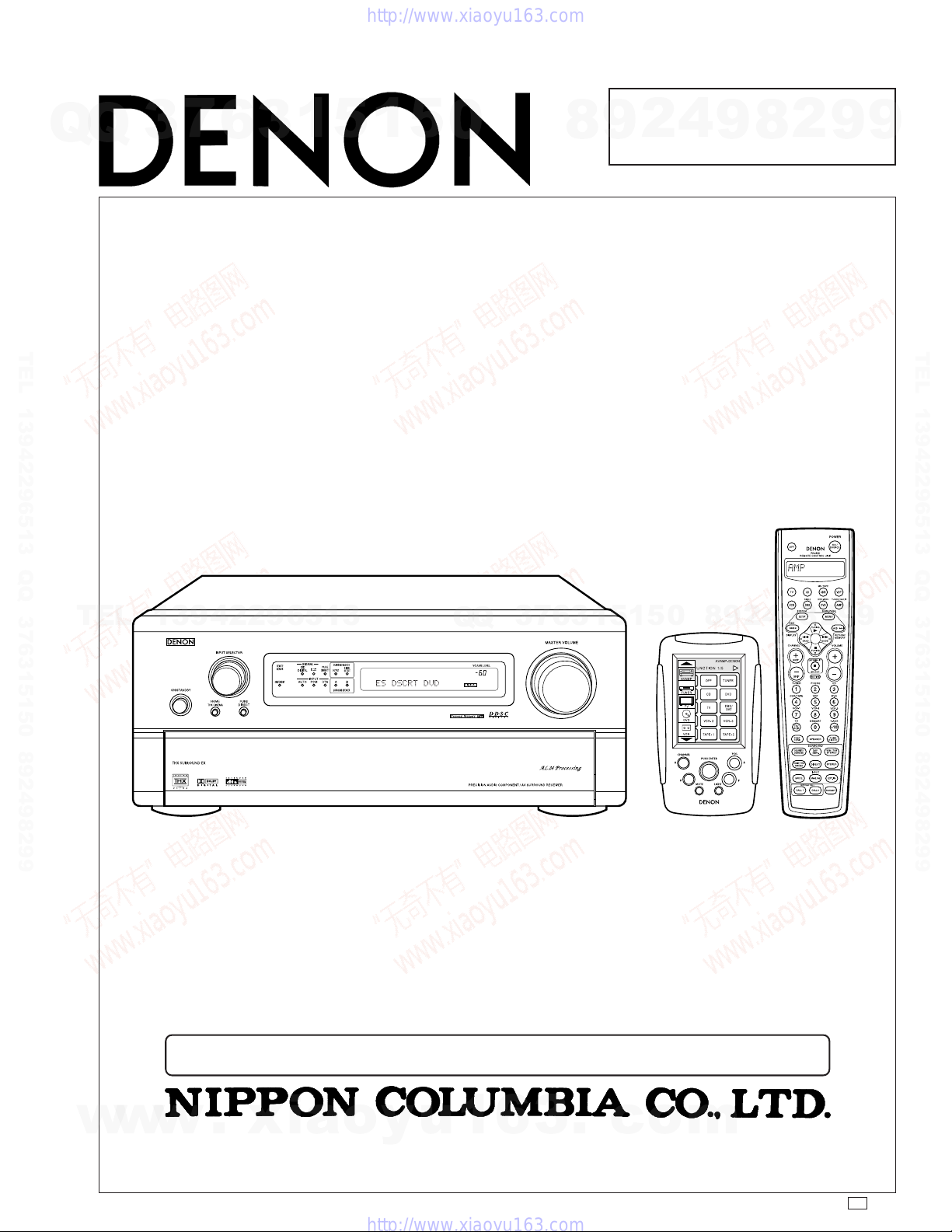
Hi-Fi Component
8
2
9
9
MODEL
TEL 13942296513 QQ 376315150 892498299
MODEL
AV SURROUND RECEIVER / AMPLIFIER
TEL
13942296513
AVR-4802
AVC-A11SR
7
3
Q
Q
6
3
1
5
1
5
0
8
9
2
4
9
8
2
9
TEL 13942296513 QQ 376315150 892498299
9
w
w
For AVR-4802 For AVC-A11SR
Some illustrations using in this service manual are slightly different from the actual set.
w
.
xia
o
y
u
1
6
3
.
c
o
14-14, AKASAKA 4-CHOME, MINATO-KU, TOKYO 107-8011 JAPAN
Telephone: 03 (3584) 8111
m
X0120 1174 NC 0108
Page 2
SAFETY PRECAUTIONS
The following check should be performed for the continued protection of the customer and service technician.
7
Q
Q
TEL 13942296513 QQ 376315150 892498299
TEL
3
LEAKAGE CURRENT CHECK
Before returning the unit to the customer, make sure you make either (1) a leakage current check or (2) a line to chassis
resistance check. If the leakage current exceeds 0.5 milliamps, or if the resistance from chassis to either side of the
power cord is less than 460 kohms, the unit is defective.
SPECIFICATIONS
Audio Section
Power amplifier:
Rated output: Stereo (2 ch driven)
(All properties shown are only for the 125 W + 125 W (8 Ω/ohms, 20 Hz ~ 20 kHz with 0.05 % T.H.D.)
power amplifer stage.) 150 W + 150 W (6 Ω/ohms, 20 Hz ~ 20 kHz with 0.05 % T.H.D.)
Dynamic power: 170 W × 2 ch (8 Ω/ohms)
Output terminals: Front/Center: 6 ~ 16 Ω/ohms
Analog:
Input sensitivity/input impedance: 200 mV/47 kΩ/kohms
Frequency response: 10 Hz ~ 100 kHz: +0, −3 dB (DIRECT mode)
S/N: 105 dB (DIRECT mode)
Distortion: 0.005 % (20 Hz ~ 20 kHz) (DIRECT mode)
Rated output/maximum output: 1.2 V/8 V
Digital:
D/A output: Rated output 2 V (at 0 dB playback)
Digital input: Format Digital audio interface
Phono equalizer (PHONO input
Input sensitivity: 2.5 mV
RIAA deviation: ±1 dB (20 Hz to 20 kHz)
Signal-to-noise ratio: 74 dB (A weighting, with 5 mV input)
Rated output/Maximum output: 150 mV/8V
Distortion factor: 0.03 % (1 kHz, 3 V)
13942296513
Video Section
Standard video jacks
Input/output level and impedance: 1 Vp-p, 75 Ω/ohms
Frequency response: 5 Hz ~ 10 MHz +0, −3 dB
S-video jacks
Input/output level and impedance: Y (brightness) signal 1 Vp-p, 75 Ω/ohms
Frequency response: 5 Hz ~ 10 MHz +0, −3 dB
Color component video terminal:
Input/output level and impedance: Y (brightness) signal 1 Vp-p, 75 Ω/ohms
Frequency response: DC ~ 50 MHz +0, −3 dB
Tuner Section
Receiving range: 87.5 MHz ~ 107.9 MHz 520 kHz ~ 1710 kHz
Usable sensitivity: 1.0 µV (11.2 dBf) 18 µV
50 dB Quieting sensitivity: MONO 1.6 µV (15.3 dBf)
Signal to Noise Ratio (IHF-A): MONO 77 dB 50 dB
Total Harmonic Distortion (at 1 kHz): MONO 0.15 %
General
Power supply: AC 120 V, 60 Hz (U.S.A., Canada & Taiwan R.O.C. model)
Power consumption: 10.5 A (U.S.A., & Canada model)
6
3
1
5
REC OUT):
1
5
0
270 W × 2 ch (4 Ω/ohms)
350 W × 2 ch (2 Ω/ohms)
Surround: A or B 6 ~ 16 Ω/ohms
Total harmonic distortion 0.005 % (1 kHz, at 0 dB)
S/N ratio 110 dB
Dynamic range 108 dB
Q
Q
C (color) signal 0.286 Vp-p, 75 Ω/ohms
P
B/CB (blue) signal 0.7 Vp-p, 75 Ω/ohms
P
R/CR (red) signal 0.7 Vp-p, 75 Ω/ohms
[FM] (note: µV at 75 Ω/ohms, 0 dBf = 1 × 10
STEREO 23 µV (38.5 dBf)
STEREO 72 dB
STEREO 0.3 %
AC 230 V, 50 Hz (Europe & Asia model)
AC 220 V, 50 Hz (China model)
A + B 8 ~ 16 Ω/ohms
7
3
6
8
3
9
1
5
4
2
0
5
1
-15
W) [AM]
AVR-4802/AVC-A11SR
9
8
9
8
2
4
2
9
8
2
9
9
9
9
TEL 13942296513 QQ 376315150 892498299
Maximum external dimensions: 434 (W) × 179 (H) × 485 (D) mm (17-3/32″ × 7-3/64″ × 19-3/32″)
Mass: 20.5 kg (45 lbs 3.1 oz)
Remote Control Unit (RC-8000): AVR Model only
Batteries: LR6/AA Type (four batteries)
External dimensions: 96 (W) × 38 (H) × 168.5 (D) mm (3-25/32″ × 1-1/2″ × 6-41/64″)
Mass: 242 g (Approx. 8.5 oz) (not including batteries)
Remote Control Unit (RC-899): AVC Model only
w
Batteries: R6P/AA Type (three batteries)
w
w
External dimensions: 61 (W) × 230 (H) × 34 (D) mm (2-13/32″ × 9-1/16″ × 1-11/32″)
Mass: 150 g (Approx. 5.3 oz) (not including batteries)
* For purposes of improvement, specifications and design are subject to change without notice.
.
xia
o
y
u
1
6
3
.
c
o
m
2
Page 3
Q
CAUTION IN SERVICING
When you have replaced the 1U-3291 Unit, or changed the CPU, DSP, or their peripheral parts, be sure to perform “RESET”
by pressing S803 on the DSP Unit Ass’y in the state of Standby or Power-on.
Q
WIRE ARRANGEMENT
If wire bundles are untied or moved to perform adjustment or parts replacement etc.,be sure to rearrange them neatly as they
were originally bundled or placed afterward.
Otherwise, incorrect arrangement can be a cause of noise generation.
Wire arrangement viewed from the top
3
7
6
3
1
5
1
5
0
8
9
2
AVR-4802/AVC-A11SR
4
9
8
2
9
9
TEL 13942296513 QQ 376315150 892498299
TEL
13942296513
Front Panel side
7
3
Q
Q
6
3
1
5
1
5
0
8
9
2
4
9
8
2
9
TEL 13942296513 QQ 376315150 892498299
9
w
w
w
.
xia
o
y
u
1
6
Back Panel side
3
.
c
o
m
3
Page 4
AVR-4802/AVC-A11SR
Q
TEL 13942296513 QQ 376315150 892498299
Wire arrangement viewed from the bottom
Q
3
7
6
3
1
5
1
5
0
Front Panel side
8
9
2
4
9
8
2
9
9
TEL 13942296513 QQ 376315150 892498299
TEL
13942296513
7
3
Q
Q
Back Panel side
6
3
1
5
1
5
0
8
9
2
4
9
8
2
9
9
w
w
w
.
xia
o
y
u
1
6
3
.
c
o
m
4
Page 5

Q
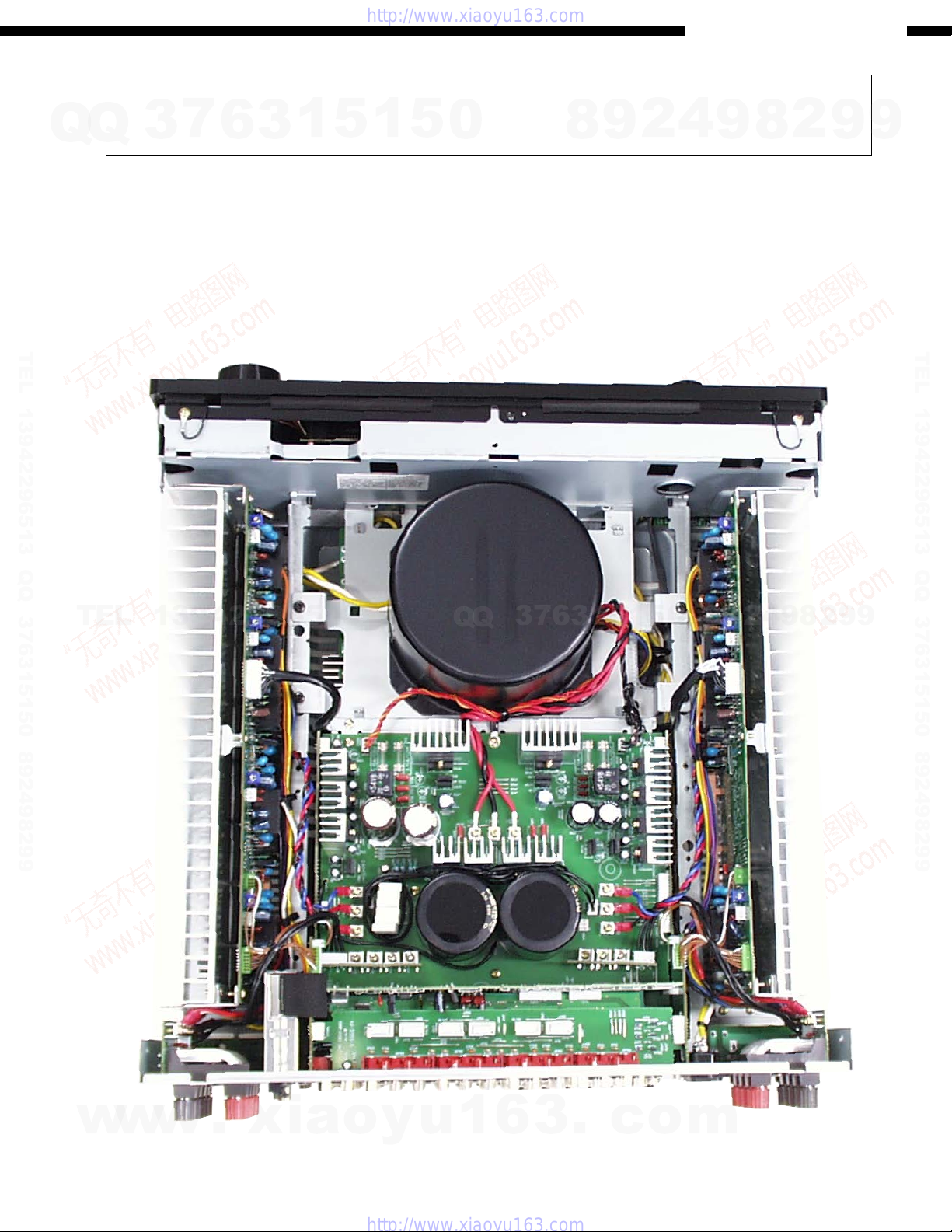
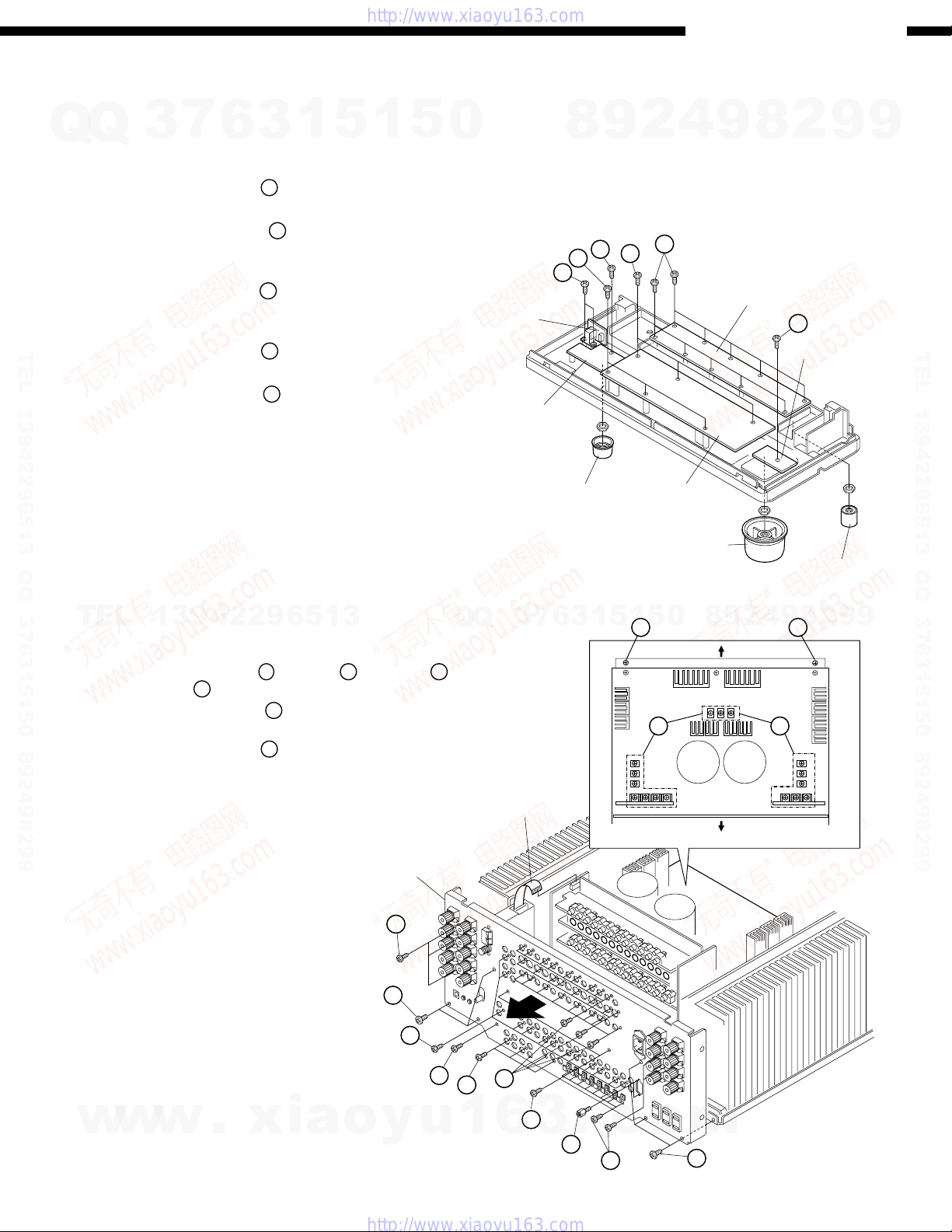
DISASSEMBLY
(Follow the procedure below in reverse order when reassembling)
7
Q
3
Top Cover
(1) Remove 9 screws 1 on both sides and on the top.
(2) Remove 4 screws
Cover by sliding to the arrow direction.
6
1
5
1
3
on the rear and detach the Top
2
5
0
1
1
8
9
2
Top Cover
AVR-4802/AVC-A11SR
4
9
8
2
2
9
9
TEL 13942296513 QQ 376315150 892498299
Front Panel
TEL
13942296513
(1) Remove 11 screws 3 and detach the Bottom Cover.
(2) Remove the screw
(3) Disconnect FFC wire from its connector, and detach
the Front Panel in the arrow direction.
3
, 7 screws 5.
4
Q
Q
3
7
6
5
3
1
5
4
1
5
0
8
5
9
2
4
9
1
8
2
9
TEL 13942296513 QQ 376315150 892498299
2
1
9
w
w
w
.
xia
Front Panel
FFC Wire
o
y
u
1
6
3
.
5
c
o
m
5
Page 6
AVR-4802/AVC-A11SR
7
Q
Q
TEL 13942296513 QQ 376315150 892498299
3
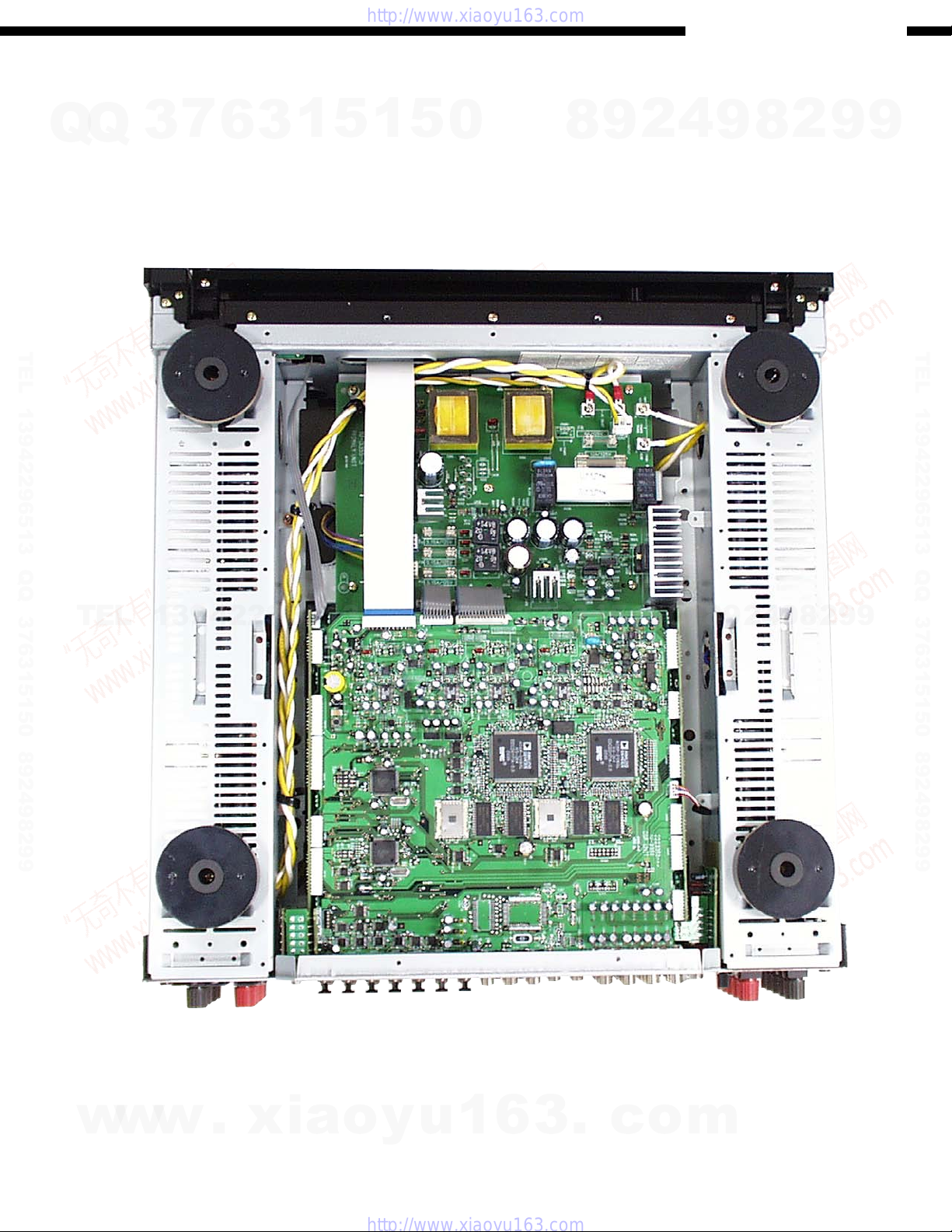
P.W.B.s on Front Panel
(1) FLD P.W.B.
Remove 6 screws
(2) Tact SW P.W.B.
Remove 10 screws
and nut.
(3) Master VR P.W.B.
Remove the screw 8 after taking off the master volume
knob and nut.
(4) Power SW P.W.B.
Remove 2 screws
(5) Remo-con. P.W.B.
Remove the screw
knob and nut.
6
1
5
1
3
.
6
after taking off the select knob
7
.
9
after taking off the input selector
10
5
0
Power SW
P.W.B.
Remo-con. P.W.B.
8
6
9
4
2
9
10
Master Volume Knob
7
6
FLD P.W.B.Input Selector Knob
8
9
Tact SW P.W.B.
2
9
8
Master Volume
P.W.B.
Select Knob
9
TEL 13942296513 QQ 376315150 892498299
S. Video P.W.B. / C. Video P.W.B. / Comp
TEL
Video P.W.B. / Audio P.W.B. Block
13942296513
(1) Disconnect the FFC from its connector.
(2) Remove 6 screws 11, 3 screws 12, 53 screws 13, 2
screws 14, and detach the Back Panel.
(3) Remove 16 screws 15 of the wires connecting to the
C. Video P.W.B.
(4) Remove 2 screws 16.
Back Panel
13
11
13
Q
Q
7
3
FFC Wire
5
1
3
6
C.Video P.W.B. (Top view)
1
16
5
15
0
Front
Rear
8
9
2
4
15
9
16
8
2
9
9
w
w
w
.
xia
12
o
y
u
13
1
13
6
13
3
14
.
c
13
o
m
11
6
Page 7
17
AVR-4802/AVC-A11SR
7
Q
Q
TEL 13942296513 QQ 376315150 892498299
3
P.W.B. Block
Remove P.W.B.s in the following order.
1. Connect L P.W.B.
2. Comp. Video P.W.B.
3. S Video P.W.B./C Video & Reg. P.W.B./OSD P.W.B.
4. Audio In P.W.B.
5. DSP P.W.B.
6
3
1
5
1
CONNECT R P.W.B.
COMP. VIDEO P.W.B.
S VIDEO P.W.B.
PHONO P.W.B.
5
0
AUDIO IN P.W.B.
8
2
9
OSD P.W.B.
4
8
9
C VIDEO & REG. P.W.B.
2
CONNECT L P.W.B.
9
9
TEL 13942296513 QQ 376315150 892498299
TEL
Power AMP L/R P.W.B.
13942296513
(1) Remove 8 screws 17 fastening to the chassis.
Q
Q
DSP P.W.B.
6
7
3
3
1
5
1
5
17
0
17
232C P.W.B.
2
9
8
4
9
8
2
9
17
9
w
w
w
.
xia
o
y
u
1
6
3
.
c
o
m
7
Page 8
AVR-4802/AVC-A11SR
7
Q
Q
TEL 13942296513 QQ 376315150 892498299
3
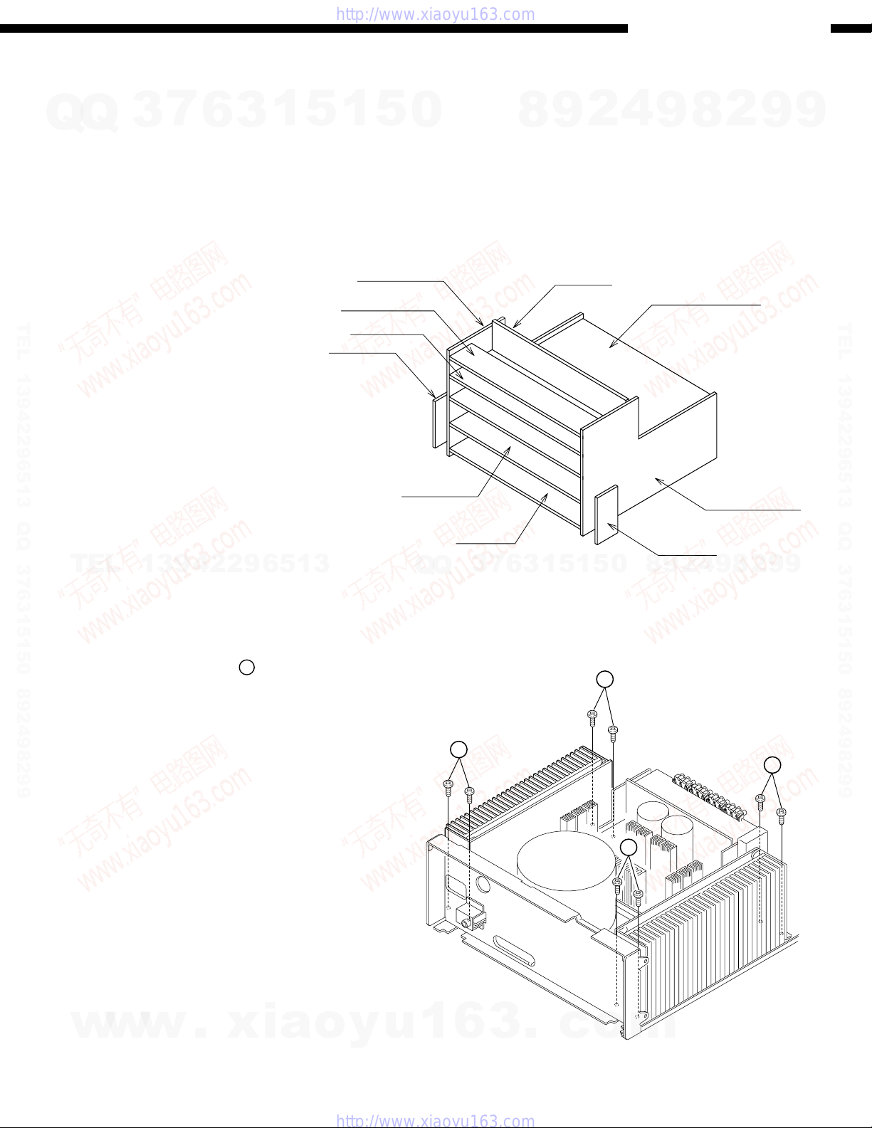
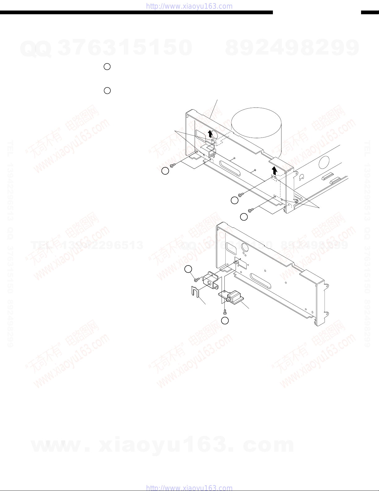
Front Chassis, H/P P.W.B.
(1) Remove 8 screws 18.
(2) Detach the Front Chassis by pulling upward to release
4 hooks.
(3) Remove 2 screws 19 and snap plate, then detach the
H/P P.W.B.
6
3
1
5
1
5
Hook
18
0
Front Chassis
8
18
9
18
2
4
9
8
2
Hook
9
9
TEL 13942296513 QQ 376315150 892498299
TEL
13942296513
Q
Q
19
7
3
Snap Plate
6
19
3
1
1
5
H/P P.W.B.
5
0
8
9
2
4
9
8
2
9
9
w
w
w
.
xia
o
y
u
1
6
3
.
c
o
m
8
Page 9
1
3
2
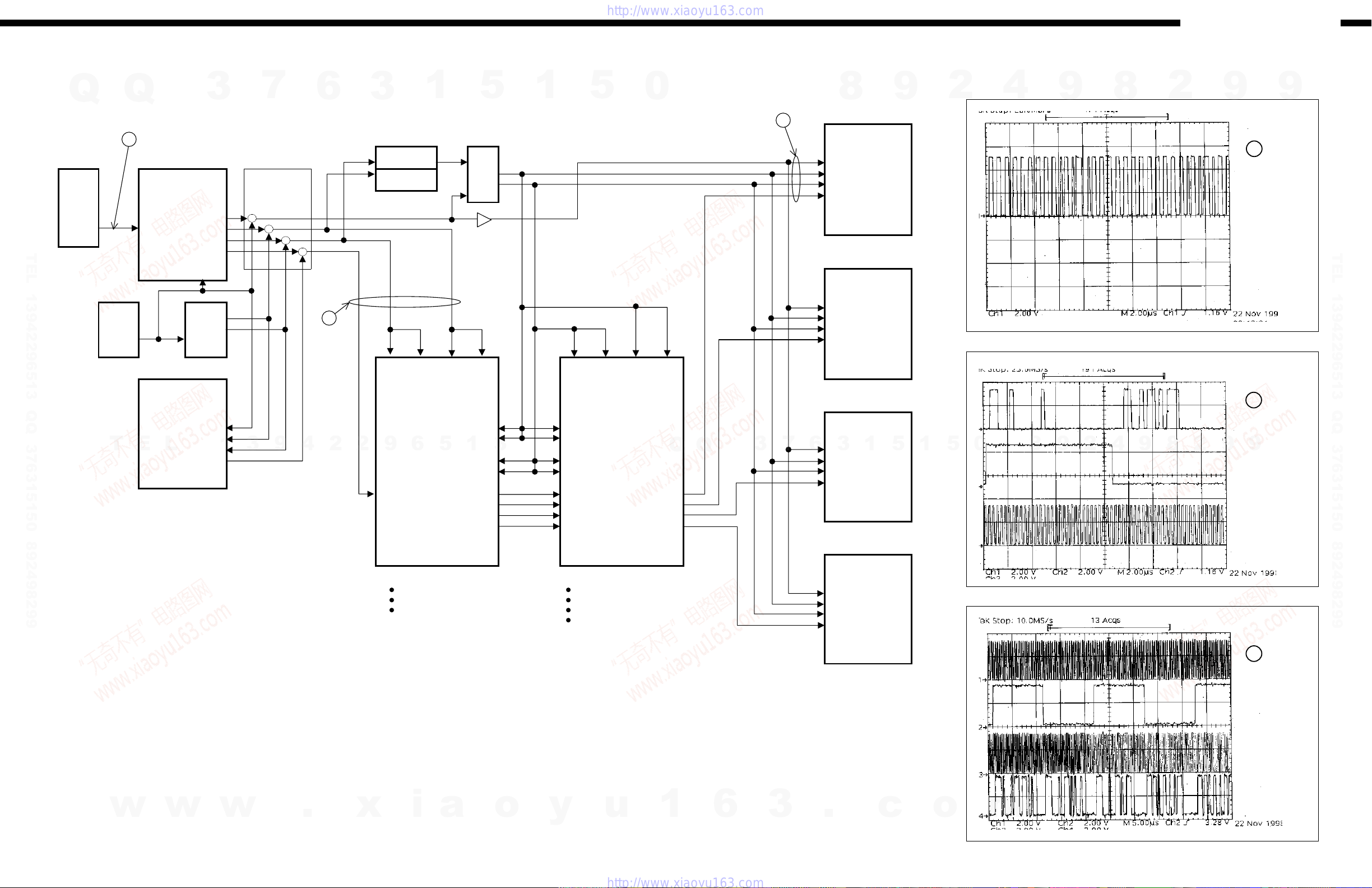
IC512
1
SN74LV4040APW
INPUT
SELECTOR (9) (3)
(11)
(2)MCLK
(10)
(7)
(26)BCLK
IC104
(13)
(25)LRCLK
SN74HC
(10)
(27)SDATA
151APW
CKOUT(13) FRONTch
(5) (5)DIN2 BCK(14)
LRCK(15)
DATAD(16)
XIN(22)
12.287MHz
IC113
(2)MCLK
SG-8002
(7) (26)BCLK
(13) (25)LRCLK
(3) (10) (27)SDATA
IC112 CENTERch
SN74LV4040APW
(2) (13) (4) (15)
(7) (18) (8) (19)
SUBWOOFERch
RFS0 RFS1 RCLK0 RCLK1
TFS0 TFS1 TCLK0 TCLK1
MCLK(17)
TCLK0(8)
(4)RCLK0
AIN SCLK(18)
TCLK1(19)
(15)RCLK1
LRCK(19) (2)MCLK
SDATA(21) TFS0(7) (2)RFS0 (26)BCLK
TFS1(18)
(13)RFS1
(25)LRCLK
(27)SDATA
(5)DR0A
DT0A(11)
(5)DR0A
DT0A(11)
DT0B(12)
(6)DR0B
DT0B(12)
SURROUNDch
DT1A(22)
(16)DR1A
DT1A(22)
DT1B(23)
(17)DR1B
DT1B(23)
(2)MCLK
(26)BCLK
(25)LRCLK
(27)SDATA
SURROUND BACKch
DIR
IC111
LC89055W
A/D CONVERTER
AD1854K
IC114
AK5353VS
IC107
74LVX157MTC
2nd DSP1st DSP
A/D SELECTOR
IC502
ADSP-21065L
IC501
ADSP-21065L
IC511
D/A CONVERTER
IC305
AD1854K
IC307
IC301
AD1854K
IC303
AD1854K
SYNC
SN74LV86APW
SN74LV00APW
IC523
256fs
64fs
fs
DATA
DATA
256fs
64fs
fs
FRONT
CENTER/SW
SURROUNDSURROUND BACK
fs
64fs
2
3
DOLBY DIGITAL Decode
DTS-ES Decode
AL24 Processing
THX Filter Processing
EX/ES Matrices Processing
Sound Simulation
Bus-Management Processing
* fs is a sampling frequency of input digital signal.
e.g.: sampling frequency 48 kHz → fs=48 kHz
* 64fs and 256fs are 64 or 256 times the sampling frequency
respectively.
e.g.:sampling frequency 48 kHz
64fs:48kHz x 64 = 3.072MHz
256fs:48kHz x 256 = 12.288MHz
* The sampling frequency for analog input is fixed to 48kHz internally.
* (No.) indicates the pin number of individual IC.
* The arrow indicates the direction of signal flow. As the input terminal
pointed by the arrowhead and the output terminal by the opposite.
CLOCK FLOW & WAVE FORM IN DIGITAL BLOCK
Clock Flow Wave Form
Q
Q
3
7
6
3
1
5
1
5
0
8
9
2
4
9
8
AVR-4802/AVC-A11SR
2
9
9
CH1: IC104 (5)
TEL 13942296513 QQ 376315150 892498299
T
E
w
L
w
1
3
w
9
4
.
2
2
x
9
6
i
5
a
1
3
o
y
u
Q
1
Q
6
7
3
3
6
.
3
1
5
c
1
5
o
0
m
8
9
2
4
9
8
2
9
CH1: DATA
9
CH2: fs
CH3: 64fs
CH1: 64fs
CH2: fs
CH3: 256fs
CH4:
FRONT DATA
TEL 13942296513 QQ 376315150 892498299
9
Page 10
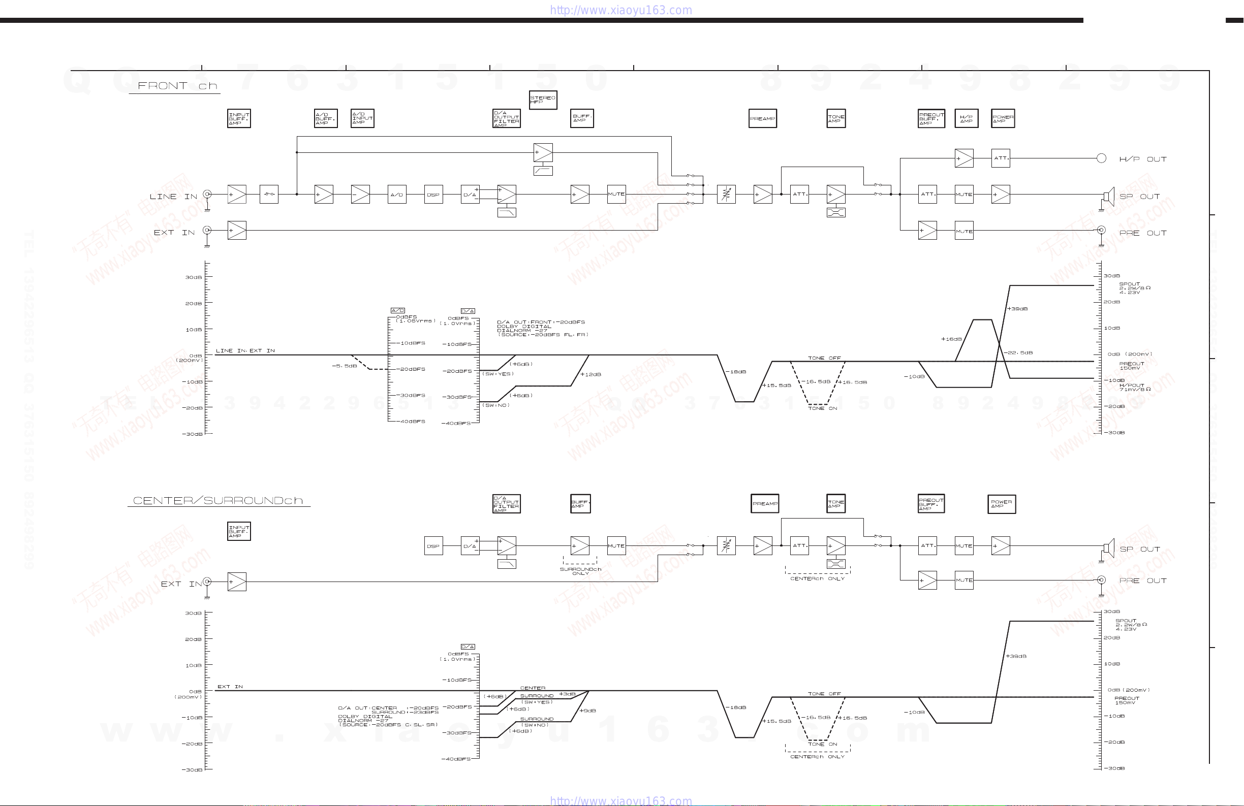
LEVEL DIAGRAMS (1/2)
1
2
3
4
5
76
AVR-4802/AVC-A11SR
8
Q
TEL 13942296513 QQ 376315150 892498299
Q
3
7
6
3
1
5
1
5
0
8
9
2
4
9
8
2
9
9
A
TEL 13942296513 QQ 376315150 892498299
B
T
E
L
1
3
9
4
2
2
9
6
5
1
3
Q
Q
3
7
6
3
1
5
1
5
0
8
9
2
4
9
8
2
9
9
C
D
w
w
w
.
x
i
a
o
y
u
1
6
3
.
c
o
E
m
10
Page 11
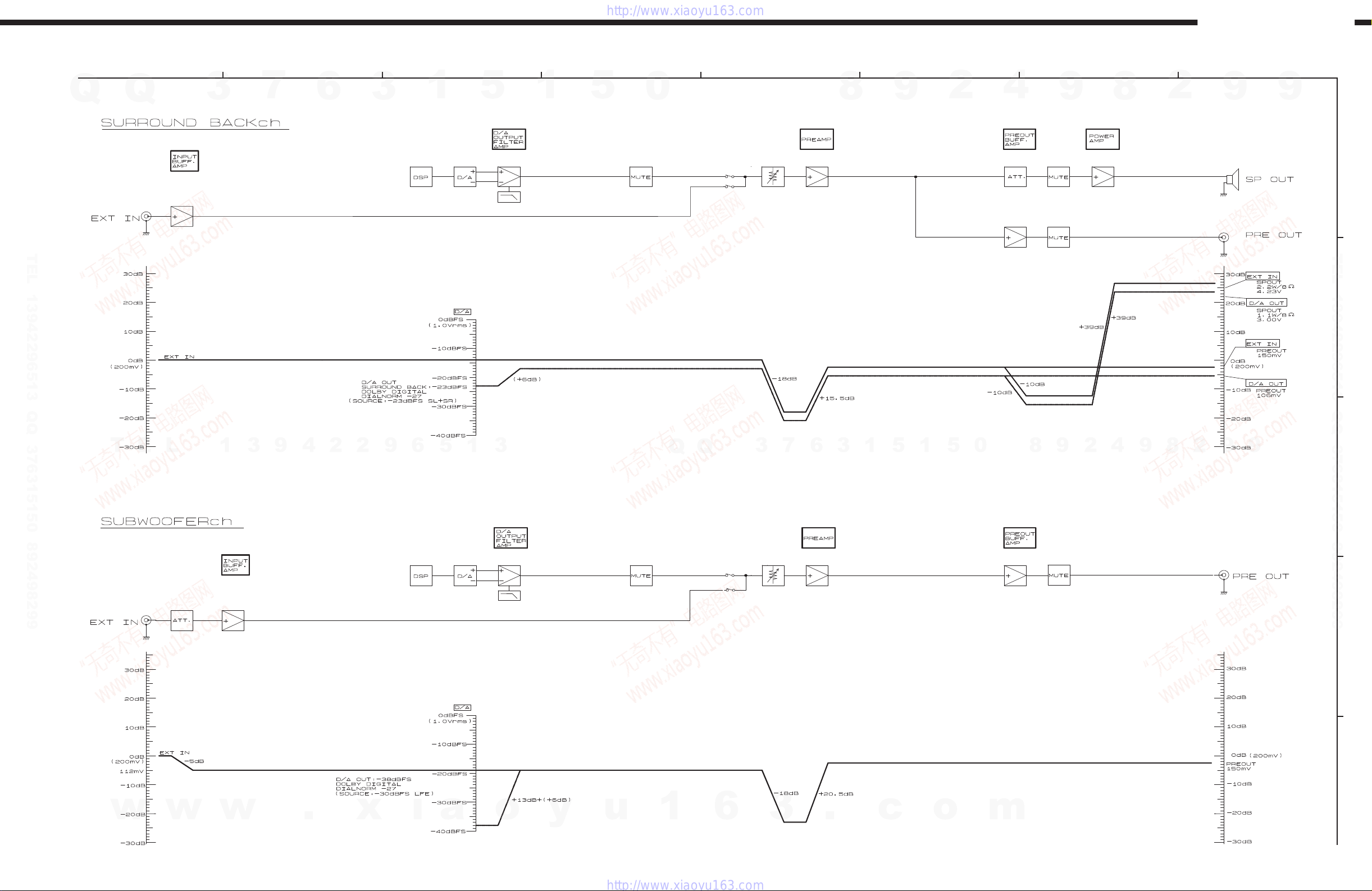
LEVEL DIAGRAMS (2/2)
1
2
3
4
5
76
AVR-4802/AVC-A11SR
8
Q
TEL 13942296513 QQ 376315150 892498299
Q
3
7
6
3
1
5
1
5
0
8
9
2
4
9
8
2
9
9
A
TEL 13942296513 QQ 376315150 892498299
B
T
E
L
1
3
9
4
2
2
9
6
5
1
3
Q
Q
3
7
6
3
1
5
1
5
0
8
9
2
4
9
8
2
9
9
C
D
w
w
w
.
x
i
a
o
y
u
1
6
3
.
c
o
E
m
11
Page 12
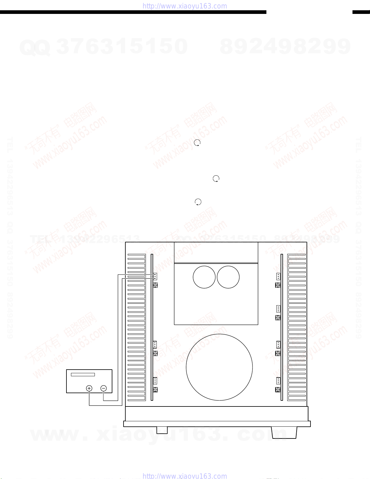
ADJUSTMENT
Audio Section
7
Q
Q
TEL 13942296513 QQ 376315150 892498299
3
Idling Current (1U-3356-1, 2)
Required measurement equipment : DC Voltmeter
Preparation
(1) Avoid direct blow from an air conditioner or an electric fan, and adjust the unit at normal room tempereture 15 °C ~ 30 °C
(59 °F ~ 86 °F).
(2) Presetting
POWER (Power source switch) → OFF
SPEAKER (Speaker terminal) → No load (Do not connect speaker, dummy resistor, etc.)
Adjustment
(1) Remove top cover and set VR101, VR301, VR401 on 1U-3356-1 (Power Amp L unit), VR102, VR202, VR302, VR402 on
1U-3356-2 (Power Amp. R Unit) at fully counterclockwise (
(2) Connect DC Voltmeter to test points (FRONT-Lch: TP101, FRONT-Rch: TP102, CENTER ch: TP202, SURROUND-Lch:
TP301, SURROUND-Rch: TP302, SURROUND BACK-Lch: TP401, SURROUND BACK-Rch: TP402).
(3) Connect power cord to AC Line, and turn power switch "ON".
6
3
1
5
1
5
0
) position.
8
9
2
AVR-4802/AVC-A11SR
4
9
8
2
9
9
TEL 13942296513 QQ 376315150 892498299
(4) Presetting. MASTER VOLUME : "---" counterclockwise (
MODE : 5CH/7CH STEREO
FUNCTION : CD
(5) Within 2 minutes after the power on, turn VR101 clockwise (
(6) After 10 minutes from the preset above, turn VR101 to set the voltage to 2 mV ±0.5 mV DC.
(7) Adjust the Variable Resistors of other channels in the same way.
TEL
13942296513
1U-3356-1
TP101
VR101
TP301
Q
Q
3
min.)
) to adjust the TEST POINT voltage to 2 mV ±0.5 mV DC.
1
5
1
3
6
7
0
5
1U-3356-2
8
TP102
VR102
TP202
VR202
TP302
9
2
4
9
8
2
9
9
w
w
w
DC Voltmeter
.
xia
VR301
Power Trans
TP401
VR401
o
y
u
1
6
3
.
c
o
VR302
TP402
VR402
m
12
Page 13
Q
SEMICONDUCTORS
IC’s
7
Q
3
LH28F800BVE-BTL90 (IC504, 507)
6
3
1
5
1
5
0
8
9
2
AVR-4802/AVC-A11SR
4
9
8
AVR-4802
2
9
9
1
A15
2
A14
3
A13
4
A12
5
A11
6
A10
7
A9
8
A8
9
NC
10
NC
11
WE
12
RESET
13
NC
14
NC
RDY/BSY
TEL 13942296513 QQ 376315150 892498299
N74AHCT573PW (IC516, 520)
N74LV573ANS (IC517, 521)
TEL
GND
15
16
A18
17
A17
18
A7
19
A6
20
A5
21
A4
22
A3
23
A2
24
A1
1
OE
2
D0
3
D1
4
D2
5
13942296513
D3
6
D4
7
D5
8
D6
9
D7
10
20
Vcc
19
Q0
Q1
18
17
Q2
16
Q3
Q4
15
Q5
14
13
Q6
Q7
12
11
LE
48
47
46
45
44
43
42
41
40
39
38
37
36
35
34
33
32
31
30
29
28
27
26
25
A16
BYTE
SS
V
DQ15/A-1
DQ7
DQ14
DQ6
DQ13
DQ5
DQ12
DQ4
DD
V
DQ11
DQ3
DQ10
DQ2
DQ9
DQ1
DQ8
DQ0
OE
SS
V
CE
A0
LE
OE
Symbol Function
A0~A18 Address input
DQ0~DQ14 Data in/output
DQ15/A-1 Data in/output/Address input
CE Chip enable input
OE Output enable input
BYTE Word/byte select input
WE Write enable input
RDY/BSY Ready/busy output
RESET Hardware reset input
N.C. No connection
VDD Power
Vss GND
34
D
Q
Q
Q
L
Q0 Q1
D1 D2
D
Q
7
3
L
1819
D0
2
11
1
D3 D4 D5 D6
5678
D
6
L
Q
3
D
1
17
Q2
Q
1
5
L
Q3 Q4
D
5
TEL 13942296513 QQ 376315150 892498299
D7
9
D
Q
0
L
1516
D
Q
Q
4
2
9
8
L
L
Q5 Q6 Q7
9
D
8
L
Q
121314
2
9
9
16MB SDRAM TSOP-8 H/W (IC505, 506, 508, 509)
A4
w
w
A3
A2
A1
A0
CE
I/O 1
I/O 2
I/O 3
I/O 4
V
DD
GND
I/O 5
I/O 6
I/O 7
I/O 8
WE
A15
A14
A13
A12
N.C.
w
1
2
3
4
5
6
7
8
9
10
11
12
13
14
15
16
17
18
19
20
21
22
.
xia
A5
44
A6
43
A7
42
OE
41
UB
40
LB
39
I/O 1 6
38
I/O 1 5
37
I/O 1 4
36
I/O 1 3
35
GND
34
V
33
32
31
30
29
28
27
26
25
24
23
DD
I/O 1 2
I/O 1 1
I/O 1 0
I/O 9
N.U.
A8
A9
A10
A11
N.C.
o
y
Symbol Function
A0~A15 Address input
I/O1~I/O16 Data in/output
CE Chip enable input
WE Write enable input
OE Output buffer control input
LB, UB Data byte control input
VDD Power terminal (3.3V)
GND GND
N.C. No connection
N.U. Unusable (input)
u
1
6
3
.
c
o
m
13
13
Page 14
ADSP-21065L (IC501, 502)
AVR-4802/AVC-A11SR
Q
Q
3
7
6
3
1
5
1
1
5
0
TEL 13942296513 QQ 376315150 892498299
52
53
ADSP-21065L Terminal Function
Q
Q
1
Pin
Pin Name
No.
106 GND
107 DATA15
108 DATA16
109 DATA17
110 VDD
111 DATA18
112 DATA19
7
3
113 DATA20
114 GND
115 NC
116 DATA21
117 DATA22
118 DATA23
119 GND
120 VDD
121 DATA24
122 DATA25
123 DATA26
124 VDD
125 GND
126 DATA27
127 DATA28
128 DATA29
129 GND
130 VDD
131 VDD
132 DATA30
133 DATA31
134 FLAG7
135 GND
136 FLAG6
137 FLAG5
138 FLAG4
139 GND
6
3
140 VDD
Pin
No.
1 VDD
2 RFS0
3 GND
4 RCLK0
5 DR0A
6 DR0B
7 TFS0
TEL
8 TCLK0
9 VDD
10 GND
11 DT0A
12 DT0B
13 RFS1
14 GND
15 RCLK1
16 DR1A
17 DR1B
18 TFS1
19 TCLK1
20 VDD
21 VDD
22 DT1A
23 DT1B
24
25 GND
26
27 BR1
28 BR2
29 VDD
30 CLKIN
31 XTAL
32 VDD
33 GND
34 SDCLK1
w
w
35 GND
Pin
Pin Name
13942296513
PWM_EVENT1
PWM_EVENT0
w
.
Pin Name
No.
36 VDD
37 SDCLK0
38 DMAR1
39 DMAR2
40 HBR
41 GND
42 RAS
43 CAS
44 SDWE
45 VDD
46 DQM
47 SDCKE
48 SDA10
49 GND
50 DMAG1
51 DMAG2
52 HBG
53 BMSTR
54 VDD
55 CS
56 SBTS
57 GND
58 WR
59 RD
60 GND
61 VDD
62 GND
63 REDY
64 SW
65 CPA
66 VDD
67 VDD
68 GND
69 ACK
xia
70 MS0
Pin
No.
71 MS1
72 GND
73 GND
74 MS2
75 MS3
76 FLAG11
77 VDD
78 FLAG10
79 FLAG9
80 FLAG8
81 GND
82 DATA0
83 DATA1
84 DATA2
85 VDD
86 DATA3
87 DATA4
88 DATA5
89 GND
90 DATA6
91 DATA7
92 DATA8
93 VDD
94 GND
95 VDD
96 DATA9
97 DATA10
98 DATA11
99 GND
100 DATA12
101 DATA13
102 NC
103 NC
104 DATA14
o
y
105 VDD
Pin Name
u
6
8
3
.
9
157208
156
105
104
Pin
No.
141 VDD
142 NC
143 ID1
144 ID0
145 EMU
146 TDO
147 TRST
1
5
1
148 TDI
149 TMS
150 GND
151 TCK
152 BSEL
153 BMS
154 GND
155 GND
156 VDD
157 RESET
158 VDD
159 GND
160 ADDR23
161 ADDR22
162 ADDR21
163 VDD
164 ADDR20
165 ADDR19
166 ADDR18
167 GND
168 GND
169 ADDR17
170 ADDR16
171 ADDR15
172 VDD
173 ADDR14
174 ADDR13
c
175 ADDR12
2
Pin Name
5
o
4
0
m
9
8
9
2
8
Pin
Pin Name
No.
176 VDD
177 GND
178 ADDR11
179 ADDR10
180 ADDR9
181 GND
182 VDD
2
183 ADDR8
184 ADDR7
185 ADDR6
186 GND
187 GND
188 ADDR5
189 ADDR4
190 ADDR3
191 VDD
192 VDD
193 ADDR2
194 ADDR1
195 ADDR0
196 GND
197 FLAG0
198 FLAG1
199 FLAG2
200 VDD
201 FLAG3
202 NC
203 NC
204 GND
205 IRQ0
206 IRQ1
207 IRQ2
208 NC
4
9
8
9
2
9
9
TEL 13942296513 QQ 376315150 892498299
9
14
Page 15
75
76
100
1
25
26
50
51
AVR-4802/AVC-A11SR
TMP95FY64F (IC801)
Q
TMP95FY64F Terminal Function
Pin.
No.
TEL 13942296513 QQ 376315150 892498299
1 VREFL VREFL
2 AVss AVss
3 AVcc AVcc
4 DAOUT0 DAOUT0 No connection
5 DAOUT1 DAOUT1 O C
6 _NMI _NMI I
7 P53/_BUSRQ ASIC RESET O N
8 P54/_BUSAK WP1 O C
9 P55/_WAIT WP2 O C
10 P56/INT0 B.DOWN I
11 P57/SCLK2/_CTS2 ROM_RES1 O C
12 P80/TxD0 MISO O C MAIN-SUB µcom comm. control terminal (Data out)
13 P81/RxD0 MOSI I
14 P82/SCLK0/_CTS0 CLK I/O C MAIN-SUB µcom comm. control terminal (I2C clock in/out)
15 P83/TxD1 DIR MOSI O C
16 P84/RxD1 DIR MISO I
17 P85/SCLK1/_CTS1 DIR CLK O C
18 P86/TxD2 TxD O C
19 P87/RxD2 RxD I
20 P60/_CS0 D.EXP OE O C
21 P61/_CS1 D.EXP CLK O C
22 P62/_CS2 D.EXP DATA O C
23 P63/_CS3 D.EXP STB O C
24 CLK CLK O C
25 Vcc Vcc
26 Vss I/O1
27 X1 Xin I
28 X2 Xout O
29 _EA _EA
30 _RESET RESET I
31 P70/TI0/INT1 DSP ACK1 I
32 P71/TO1 _DSP1 RESET O C
33 P72/TO3/INT2 AC-3 RF DET. I
34 P73/TI4/INT3 DAC-192 O C
35 P74/TO5 _DSP2 RESET O C
36 P75/TO7/INT4 _REQ O C
37 P90/TI8/INT5 _ACK I
38 P91/TI9/INT6 CSI I
39 P92/TO8 EMP I
40 P93/TO9 DEEPM O C
41 P94/TIA/INT7 _CS I
42 P95/TIB/INT8 ERR I
43 P96/TOA/TOB DIR RESET O C
44 Vcc Vcc
45 P00/D0 DIT_RESET C
46 P01/D1 DIT CLK C
47 P02/D2 DIT uDATA C
48 P03/D3 DIT ST C
49 P04/D4 DIT_CS C
50 P05/D5 DIT R/W C
51 P06/D6 DH/RESET C
Q
Name
T
E
w
L
w
3
Symbol I/O Type Det Op Res Ini Function
1
w
7
E↓
3
9
E↑&L
E↓&L
E↓
E↑
E↑&L
6
Od L L No connection
Eu H H ASIC control terminal (L: Reset)
Od Memory write protect for DSP1
Od Memory write protect for DSP2
&L Eu Z
Od Memory reset for DSP1
Lv
4
Lv
Lv Eu L
&L Eu
Lv
Lv
&L Od
.
Z L DIR control terminal (LC89055Q), control data output
Z L DIR control terminal (LC89055Q), control clock output
2
Z L Data send output to external (common with 1394 data comm.)
Z L Port Expander control out for DIGITAL input switching (TC4094B)
Z L Port Expander control out for DIGITAL input switching (TC4094B)
Z L Port Expander control out for DIGITAL input switching (TC4094B)
Z L Port Expander control out for DIGITAL input switching (TC4094B)
Eu
Od L L DSP1 reset output terminal (L: Reset)
Od L L DSP2 reset output terminal (L: Reset)
Eu H L MAIN-SUB µcom comm. control terminal (L: Comm. request from SUB)
Ed L L
Z L DIR control input terminal (LC89055Q), L: Reset
Z L DIT control terminal
Z L DIT control terminal
Z L DIT control terminal
Z L DIT control terminal
Z L DIT control terminal
Z L DIT control terminal
Z L DHIVA board reset (fixed to L)
6
i
1
5
a
3
A/D ref. GND
A/D GND
AD +5V
Not used (fixed to H)
Power down detect (L: Detected)
MAIN-SUB µcom comm. control terminal (Data in)
DIR control input terminal (LC89055Q), control data input
2
9
Data receive input from external (common with 1394 data comm.)
+5V
GND
X'tal connection
X'tal connection
Fixed to +5V
Reset input
DSP1 host interface comm. respond input (L: OK)
AC-3 RF signal detect input (L: AC-3 RF signal input)
Sets D/A to 192k
MAIN-SUB µcom comm. control terminal (L: Ack. return from MAIN)
DIR control input terminal (LC89055Q), L: PCM
H: EMP ON
DIR control input terminal (LC89055Q), L→H: Cannel status change
DIR control input terminal (LC89055Q), H: ERR
+5V
x
1
5
3
o
1
y
5
u
0
1
Q
Q
6
Pin.
No.
52 P07/D7 DMUTE C
53 P10/D8 I/O1 I/O C
54 P11/D9 I/O2 I/O C
55 P12/D10 I/O3 I/O C
56 P13/D11 I/O4 I/O C
57 P14/D12 I/O5 I/O C
58 P15/D13 I/O6 I/O C
59 P16/D14 I/O7 I/O C
60 P17/D15 I/O8 I/O C
61 AM8/_16 Fixed to +5V
62 Vss Vss
63 Vcc Vcc
64 P27/A23 _DSP REQUEST1 O C
65 P26/A22 WRITE1 O C
66 P25/A21 _DSP REQUEST2 O C
67 P24/A20 WRITE2 O C
68 P23/A19 DSP ACK2 I
69 P22/A18 BUSY2 I
70 P21/A17 FLAG 3A I
71 P20/A16 BUSY1 I
72 P37/A15 SEL CK O C
73 P36/A14 DIR CE O C
74 P35/A13 FLAG 3B I
75 P34/A12 DAC-RESET2 O C
76 P33/A11 DIGITAL POWER O C
77 P32/A10 DIR AUTO O C
78 P31/A9 BPSYNC O C
79 P30/_B00T/A8 _B00T I
80 P47/A7 _DEMOD RESET O C
81 P46/A6 DEMOD ON O C
82 P45/A5 FGAIN O C
83 P44/A4 A/D RESET O N
7
3
84 P43/A3 DAC-RESET1 O C
85 P42/A2 DAC-DIF. DAC differential use: H
86 P41/A1 DIG. (AC3) MUTE O C
87 P40/A0 ERR MUTE_ O C
88 P50/_RD DH IN O C
89 P51/_WR DH OUT O C
90 P52/_HWR ROM_RES2 O C
91 Vss Vss
92 PA0/AN0 96K DET I
93 PA1/AN1 DHERR I
94 PA2/AN2 I
95 PA3/AN3/_ADTRG Not used (Pull down)
96 PA4/AN4 I
97 PA5/AN5 I
98 PA6/AN6 I
99 PA7/AN7 MODE-0-SUB I
100 VREFH VREFH
Note: Pin No. : Terminal number of microcomputer.
3
Name Symbol I/O Type Det Op Res Ini Function
2
5
1
o
1
9
5
“I” = Input port
“O” = Output port
“C” = CMOS output
“N” = NMOS open drain output
“P” = PMOS open drain output
“Iu” = Inner microcomputer pull up
“Id” = Inner microcomputer pull down
“Eu” = External microcomputer pull up
“Ed” = External microcomputer pull down
“H” = Outputs High Level at reset
c
“L” = Outputs Low Level at reset
“Z” = Becomes High impedance mode at reset
8
3
6
Port Name : The name entered in the data sheet of microcomputer.
Symbol : Symbolized interface function.
I/O : Input or out of part.
Type : Composition of port in case of output port.
Op : Pull up/Pull down selection information.
Det : Indicates judging state of input port. Level detection is “LV”; Edge detection is “Ed”; Detection by both shifting is “E&L”; Serial data
Res : State at reset.
detection is “S” (Serial data output is also “S”).
.
Ini : Initial output state.
Function : Function and logical level explanation of signals to be interface.
4
E↑&L
Lv
Lv
Lv
Lv
Lv Eu Z
0
Lv
Lv
Lv
Lv
Lv
Lv
Lv
m
Z L Digital input MUTE control output (same control as SELCK)
9
Z L DSP comm. terminal (ADSP21061L:D16)
Z L DSP comm. terminal (ADSP21061L:D17)
Z L DSP comm. terminal (ADSP21061L:D18)
Z L DSP comm. terminal (ADSP21061L:D19)
Z L DSP comm. terminal (ADSP21061L:D20)
Z L DSP comm. terminal (ADSP21061L:D21)
Z L DSP comm. terminal (ADSP21061L:D22)
Z L DSP comm. terminal (ADSP21061L:D23)
GND
+5V
ZL
Z L DSP1 comm. control terminal (H: DATA WRITE)
ZL
Z L DSP2 comm. control terminal (H: DATA WRITE)
Z L ADC/DIR data/clock switching control terminal (L: ADC)
Z L DIR control terminal (LC89055Q), control chip enable output
Od L H DAC control terminal (L: Power down,↑: Reset, H: Normal)
Z L DIGITAL power ON/OFF switching
Od Z L
ZL
Od L L Demodulator reset output (L: Reset)
Od L L Demodulator osc. control output (H: Osc.)
Z L IV AMP GAIN switching control output (L: Sub-woofer on)
Eu H H A/D control terminal (L: Reset)
8
Od L H DAC control terminal (L: Power down,↑: Reset, H: Normal)
Od Z L Digital mute control output (L: AC-3 or DTS decode possible)
Od L L Pop noise preventive mute control output
Z L For 1394 (fixed to L)
Z L For 1394 (fixed to L)
Od Memory reset for DSP2
DSP1 (ADSP21061L-A:IRQ 1_) host interface interrupt req. output, L: REQ
DSP2 (ADSP21061L-A:IRQ 1_) host interface interrupt req. output, L: REQ
DSP2 host interface comm. respond input (L: OK)
DSP busy check flag (ADSP21061L-B:FLAG 2B) input, L: Normal
Special flag for ROM update (ADSP21061L-A:FLAG 3A)
DSP busy check flag (ADSP21061L-A:FLAG 2A) input, L: Normal
Special flag for ROM update (ADSP21061L-A:FLAG 3B)
Single Chip/Single Boot switching input (H & Reset: Single Chip Mode)
2
9
GND
96k signal detect input, H: 96k
DHIVA board error input (fixed to L)
Not used (Pull down)
Not used (Pull down)
Not used (Pull down)
Not used (Pull down)
FLASH ROM rewrite mode input
AD ref. +5V
8
4
9
2
8
2
9
9
9
TEL 13942296513 QQ 376315150 892498299
9
15
Page 16
75
76
100
1
25
26
50
51
AVR-4802/AVC-A11SR
TMP95FY64F (IC802)
Q
Q
3
7
6
TMP95FY64F Terminal Function
Pin.
No.
TEL 13942296513 QQ 376315150 892498299
1 VREFL VREFL
2 AVss AVss
3 AVcc AVcc
4 DAOUT0 DAOUT0 O
5 DAOUT1 DAOUT1 O
6 _NMI _NMI I
7 P53/_BUSRQ ACK O C
8 P54/_BUSAK REQ I
9 P55/_WAIT PLFL DATA O C
10 P56/INT0 PROTECT I
11 P57/SCLK2/_CTS2 PLFL CLK O C
12 P80/TxD0 PLL STB O C
13 P81/RxD0 ERROR LED O C
14 P82/SCLK0/_CTS0
15 P83/TxD1 MOSI O C
16 P84/RxD1 MISO I
17 P85/SCLK1/_CTS1 CLK I/O (C)
18 P86/TxD2 TxD O C
19 P87/RxD2 RxD I
20 P60/_CS0 FUNC/TONE CLK O C
21 P61/_CS1 FUNC/TONE DATA O C
22 P62/_CS2 ST/MONO O C
23 P63/_CS3 STANDBY O C
24 CLK CLK O C
25 Vcc Vcc
26 Vss Vss
27 X1 X1 I
28 X2 X2 O
29 _EA _EA I
30 _RESET _RESET I
31 P70/TI0/INT1 VIDEO POWER O C
32 P71/TO1 DIGITAL POWER O C
33 P72/TO3/INT2 (VKK POWER) O
34 P73/TI4/INT3 SEL A (M) I
35 P74/TO5 SEL B (M) I
36 P75/TO7/INT4 (FAN CONTROL) O C
37 P90/TI8/INT5 B.DOWN I
38 P91/TI9/INT6 STEREO I
39 P92/TO8 TUNED I
40 P93/TO9 S MONI.DET I
41 P94/TIA/INT7 REMOCON I
42 P95/TIB/INT8 S SIG.DET I
43 P96/TOA/TOB SYNC.DET I
44 Vcc Vcc
45 P00/D0 POWER O C
46 P01/D1 V.EXP OE O C
47 P02/D2 V.EXP CLK O C
48 P03/D3 V.EXP DATA O C
49 P04/D4 V.EXP STB O C
50 P05/D5 SP.EXP OE O C
51 P06/D6 SP.EXP CLK O C
52 P07/D7 SP.EXP DATA O C
Name Symbol I/O Type Det Op Res Ini Function
T
E
w
MULTI ROOM POWER
L
w
1
w
Lv Eu Z
E↑&L Ed Z
OC
3
Lv
9
4
Lv
Lv Iu L
Lv Eu Z
Lv Eu Z
E↓&L Eu Z
Lv Eu Z
Lv Eu Z
Lv Eu Z
E↑
&L Ed Z
Lv Eu Z
Lv Eu Z
.
Z
Z L PLL & FL control terminal (LC72131 & LC7511NE)
Z L PLL & FL control terminal (LC72131 & LC7511NE)
Z L PLL control terminal (LC72131)
Ed Z H Not used
Z L Power amp control terminal for MULTI ROOM (H: ON)
Z L MAIN-SUB µcom comm. control terminal
Z
Z
Z L Data transfer terminal to external
2
Z
Z L Clock output for Function switching/Tone IC control
Z L Data output for Function switching/Tone IC control
Z L Stereo/Mono control signal (L: Stereo receive)
Ed Z H Standby LED drive output (H: Light)
Z L Video power ON/OFF switching (H: ON)
Z L Digital power ON/OFF switching (H: ON)
Z L Not used (-VKK power ON/OFF switching)
Z L Not used (Fan control for power Tr)
Z H Power relay control output (H: ON)
Z L Port expander control output for video circuit (TC4094B)
Z L Port expander control output for video circuit (TC4094B)
Z L Port expander control output for video circuit (TC4094B)
Z L Port expander control output for video circuit (TC4094B)
Z L Port expander control output for speaker output (TC4094B)
Z L Port expander control output for speaker output (TC4094B)
Z L Port expander control output for speaker output (TC4094B)
6
i
1
5
a
3
A/D ref. GND
A/D GND
AD +5V
No connection
No connection
Not used (fixed to H)
MAIN-SUB µcom comm. control terminal
MAIN-SUB µcom comm. control terminal
Protection detect input (H: Detected)
MAIN-SUB µcom comm. control terminal
MAIN-SUB µcom comm. control terminal
2
9
Data receive terminal from external
No connection
+5V
GND
X'tal connection
X'tal connection
Fixed to +5V
Reset input
Master VR turn detect input (Rotary encoder)
Master VR turn detect input (Rotary encoder)
Power down detect (L: Detected)
Stereo detect (L: Received)
Tune detect (L: Tuned)
S Monitor connection detect input (L: Connected)
Remote control signal input
S signal detect input (H: Signal input)
Sync. detect input (H: External sync.)
+5V
x
5
1
3
o
1
y
5
u
0
1
Q
Q
6
Pin.
No.
53 P10/D8 SP.EXP STB O C
54 P11/D9 A.EXP OE O C
55 P12/D10 A.EXP CLK O C
56 P13/D11 A.EXP DATA O C
57 P14/D12 A.EXP STB O C
58 P15/D13 MAIN/SUB O C
59 P16/D14 RESET2 O C
60 P17/D15 E.VOL STBB O C
61 AM8/_16 AM8/_16
62 Vss Vss
63 Vcc Vcc
64 P27/A23 STB EXP OE O C
65 P26/A22 STB EXP CLK O C
66 P25/A21 STB EXP DATA O C
67 P24/A20 STB EXP STB O C
68 P23/A19 LED CLK O C
69 P22/A18 LED DATA O C
70 P21/A17 LED LE O C
71 P20/A16 LED OE O C
72 P37/A15 SEL H (T) I
73 P36/A14 SEL G (T) I
74 P35/A13 SEL F (B) I
75 P34/A12 SEL E (B) I
76 P33/A11 SEL D (I) I
77 P32/A10 SEL C (I) I
78 P31/A9 H/P DET I
79 P30/_BOOT/A8 _BOOT I
80 P47/A7 E.VOL CLK O C
81 P46/A6 E.VOL DATA O C
82 P45/A5 E.VOL STBA O C
83 P44/A4 E.VOL MULTI STB O C
7
3
84 P43/A3 O C
85 P42/A2 OSD RST O C
86 P41/A1 OSD STB O C
87 P40/A0 OSD DATA O C
88 P50/_RD OSD CLK O C
89 P51/_WR FL CE O C
90 P52/_HWR FL RST O C
91 Vss Vss
92 PA0/AN0 KEY1 I
93 PA1/AN1 KEY2 I
94 PA2/AN2 KEY3 I
95 PA3/AN3/_ADTRG KEY4 I
96 PA4/AN4 SBL LEVEL I
97 PA5/AN5 SBR LEVEL I
98 PA6/AN6 MODE I
99 PA7/AN7 MODE0 I
100 VREFH VREFH
Note: Pin No. : Terminal number of microcomputer.
3
Name Symbol I/O Type Det Op Res Ini Function
2
5
1
o
1
9
5
“I” = Input port
“O” = Output port
“C” = CMOS output
“N” = NMOS open drain output
“P” = PMOS open drain output
“Iu” = Inner microcomputer pull up
“Id” = Inner microcomputer pull down
“Eu” = External microcomputer pull up
“Ed” = External microcomputer pull down
c
“H” = Outputs High Level at reset
“L” = Outputs Low Level at reset
“Z” = Becomes High impedance mode at reset
8
3
6
Port Name : The name entered in the data sheet of microcomputer.
Symbol : Symbolized interface function.
I/O : Input or out of part.
Type : Composition of port in case of output port.
Op : Pull up/Pull down selection information.
Det : Indicates judging state of input port. Level detection is “LV”; Edge detection is “Ed”; Detection by both shifting is “E&L”; Serial data
Res : State at reset.
Ini : Initial output state.
Function : Function and logical level explanation of signals to be interface.
detection is “S” (Serial data output is also “S”).
.
4
I
Eu Z L LED driver control output (M66313)
Lv Eu Z
Lv Eu Z
Lv Eu Z
Lv Eu Z
Lv Eu Z
Lv Eu Z
Lv Eu Z
Lv Eu Z
0
Lv Eu Z
Lv Eu Z
Lv Eu Z
Lv Eu Z
Lv Eu Z
Lv Eu Z
Lv Eu Z
Lv Eu Z
m
Z L Port expander control output for speaker output (TC4094B)
9
Z L Port expander control output for audio mute and relay control (TC4094B)
Z L Port expander control output for audio mute and relay control (TC4094B)
Z L Port expander control output for audio mute and relay control (TC4094B)
Z L Port expander control output for audio mute and relay control (TC4094B)
Z L RS232C/MAIN-SUB µcom input switching
Z L SUB µcom reset output
Z L E VR control output (TC9459)
Fixed to +5V
GND
+5V
Z H Port expander control output for audio circuit IC strobe (TC4094B)
Z L Port expander control output for audio circuit IC strobe (TC4094B)
Z L Port expander control output for audio circuit IC strobe (TC4094B)
Z H Port expander control output for audio circuit IC strobe (TC4094B)
Z L LED driver control output (M66313)
Z L LED driver control output (M66313)
Z H LED driver control output (M66313)
Treble VR turn detect input (Rotary encoder)
Treble VR turn detect input (Rotary encoder)
Bass VR turn detect input (Rotary encoder)
Bass VR turn detect input (Rotary encoder)
Input selector turn detect input (Rotary encoder)
Input selector turn detect input (Rotary encoder)
H/P detect input (H: Detected)
Single Chip/Single Boot switching input (H & Reset: Single Chip Mode)
Z L E VR control output (TC9459)
Z L E VR control output (TC9459)
Z L E VR control output (TC9459)
Z L E VR control output for MULTI ROOM (TC9459)
9
8
Z L No connection
Z H OSD control terminal (M35015)
Z H OSD control terminal (M35015)
Z L OSD control terminal (M35015)
Z H OSD control terminal (M35015)
Z H FL control terminal (LC75711NE)
Z H FL control terminal (LC75711NE)
GND
Button input 1
Button input 2
Button input 3
Button input 4
SBL channel signal level detect, set to A/D input
SBR channel signal level detect, set to A/D input
Destination switching input
FLASH ROM rewrite mode input
AD ref. +5V
2
8
4
9
2
8
2
9
9
9
9
TEL 13942296513 QQ 376315150 892498299
16
Page 17
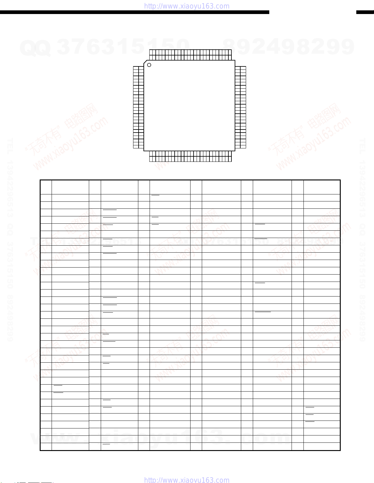
LC89055W-RA8 (IC111)
AVR-4802/AVC-A11SR
7
Q
Q
TEL 13942296513 QQ 376315150 892498299
TEL
w
3
LC89055W-RA8 Terminal Function
Pin
No.
1 DISEL I Data input terminal (select input pin of DIN0, DIN1)
2 DOUT O Input bi-phase data through output terminal
3 DIN0 I Amp built-in coaxial/optical input correspond data input terminal
4 DIN1 I Amp built-in coaxial/optical input correspond data input terminal
5 DIN2 I Optical input correspond data input terminal
6 DGND Digital GND
7 DVDD Digital power supply
8 R I VCO gain control input terminal
9 VIN I VCO free-run frequency setting input terminal
10 LPF O PLL loop filter setting terminal
11 AVDD Analog power supply
12 AGND Analog GND
13 CKOUT O Clock output terminal (256fs, 384fs, 512fs, X′tal osc., VCO free-run osc.)
14 BCK O 64fs clock output terminal
15 LRCK O fs clock output terminal (L: Rch, H: Lch, I2S: Reverse)
16 DATAO O Data output terminal
17 XSTATE O Input data detecting result output terminal
18 DGND Digital GND
19 DVDD Digital power supply
20 XMCK O X′tal osc. clock output terminal (24.576MHz or 12.288MHz)
21 XOUT O X′tal osc. connection output terminal
22 XIN I X′tal osc. connection output terminal
23 EMPHA O Emphasis information output terminal of channel status
24 AUDIO O Bit1 output terminal of channel status
25 CSFLAG O Top 40bit revise flag output terminal of channel status
26 F0/P0/C0 O Input fs cal. sig. out / data type out / input word inf. output terminal
27 F1/P1/C1 O Input fs cal. sig. out / data type out / input word inf. output terminal
28 F2/P2/C2 O Input fs cal. sig. out / data type out / input word inf. output terminal
29 VF/P3/C3 O Validity flag out / data type out / input word inf. output terminal
30 DVDD Digital power supply
31 DGND Digital GND
32 AUTO O Non PCM burst data transfer detect sig. output terminal
33 BPSYNC O Non PCM burst data preamble Pa, Pb, Pc, Pd sync sig. output terminal
34 ERROR O PLL lock error, data error flag output terminal
35 DO O CPU I/F read data output terminal
36 DI I CPU I/F write data input terminal
37 CE I CPU I/F chip enable input terminal
38 CL I CPU I/F clock input terminal
39 XSEL I Frequency select input pin of XIN X′tal osc. (24.576MHz or 12.288MHz)
40 MODE0 I Mode setting input terminal
41 MODE1 I Mode setting input terminal
42 DGND Digital GND
43 DVDD Digital power supply
44 DOSEL0 I Data output format select input terminal
45 DOSEL1 I Data output format select input terminal
w
46 CKSEL0 I Output clock select input terminal
47 CKSEL1 I Output clock select input terminal
48 XMODE I Reset input terminal
* For latch-up countermeasure, set digital (DVDD) and analog (AVDD) power on/off in the same timing.
Pin Name
13942296513
w
6
.
xia
3
I/O
1
5
o
1
y
5
u
0
Q
Q
1
3
6
7
3
8
Function
3
6
.
9
1
1
5
c
2
5
o
4
0
m
9
8
9
8
2
4
2
9
8
9
2
9
9
TEL 13942296513 QQ 376315150 892498299
9
17
Page 18
1
2
3
4
5
6
7
8
16
15
14
13
9
10
11
12
20
19
18
17
V
DD1
VERT*
HOR*
OSCIN
OSCOUT
P3
P2
P1
P0
Vss
OSC1
OSC2
CS
SCK
SIN
AC
V
DD2
CVIDEO
LECHA
CVIN
3
4
5
20
6
11
7
1
2
19 18
17
16
8
9
10
12
13
14
15
CS
SCK
SIN
V
DD1
AC
V
SS
V
DD2
OSCI
OSC2
VERT*
HOR*
INPUT
CONTROL
CIRCUIT
DATA
CONTROL
CIRCUIT
ADDRESS
CONTROL
CIRCUIT
INDICATION
OSCILLATOR
TIMING
GENERATOR
INDICATION
CONTROL
REGISTER
INDICATION RAM
INDICATION CHARACTER ROM
BLINKING CIRCUIT
SYNC SIGNAL
SWITCHING CIRCUIT
H COUNTER
INDICATION LOCATION
DETECTION CIRCUIT
READ OUT ADDRESS
CONTROL CIRCUIT
INDICATION
CONTROL CIRCUIT
SHIFT REGISTER
SYNC SIGNAL DIS-
CRIMINATING CIRCUIT
OSC CIRCUIT
FOR SYNC SIGNAL
GENERATION
TIMING
GENERATOR
NTSC
VIDEO OUTPUT
CIRCUIT
OSCIN
OSCOUT
CVIDEO
LECHA
CVIN
P0
P1
P2
P3
M35015-210SP (IC416)
AVR-4802/AVC-A11SR
Q
Q
3
7
6
3
1
5
1
5
0
TEL 13942296513 QQ 376315150 892498299
M35015-210SP Terminal Function
Pin No. Symbol Name I/O Function
1 OSC1 Osc. circuit ext. I External terminal for indication oscillator circuit. Standard OSC. freq. is approx. 7MHz.
2 OSC2 terminal. O With this OSC. freq., decides horizontal indicatin and character width.
Chip select terminal and turns to “L” when transfer serial data.
Hysteresis input. Pull up resistor is built-in.
Takes in serial data of SIN at SCK rise when CS terminal is in “L”.
Hysteresis input. Pull up rersist is built-in.
Serial input of register for indication control and data, and address for indication data
memory. Hysteresis input. Pull up rersistor is built-in.
Resets internal circuit of IC at “L” mode.
Hysteresi input. Pull up resistor is built-in.
Power supply terminal of analog system. Connect to +5V.
Output terminal of combined video signal. Outputs 2Vp-p combined signal. Character
O
output, etc. Overlap CVIN signal and outputs at superimpose.
Input terminal deciding character output level in combined video signal. color of character
I
is white.
Input terminal of external combined video signal.
I
Character output etc. overlap this external combined video signal.
Ground terminal. Connect to GND.
General output or character background signal BL NK1* output is switchable.
Polarity can be selected at ROM mask.
General output or character background signal CO1* output is switchable.
Polarity can be selected at ROM mask.
General output or character background signal BLNK2* output is switchable.
Polarity can be selected at ROM mask.
General output or character background signal CO2* output is switchable.
Polarity can be selected at ROM mask.
Inputs horizontal sync signal.
I
Hysteresis input.
I Input vertical sync signal. Hysteresis input. Polarity can be selected at ROM mask.
o
y
u
Power supply terminal of digital system. Connect to +5V.
Q
Q
1
6
TEL
w
3 CS Chip select input I
13942296513
4 SCK Serial clock input I
5 SIN Serial data input I
6 AC Auto-clear input I
DD2
7V
8CVIDEO
9 LECHA
10 CVIN
11 Vss Ground
12 P0 Output port p0 O
13 P1 Output port P1 O
14 P2 Output port P2 O
15 P3 Output port P3 O
16 OSCOUT O Terminal for external use of sync signal OSC. circuit. Use the freq.: 14.32MHz at NTSC
17 OSCIN I system, 17.73MHz at PAL. system, 14.30MHz at MPAL system.
18 HOR*
19 VERT*
w
w
DD1
20 V
Power supply
Combined
video output
Character level
input
Combined video
input
Ext. terminal
for sync sig.
OSC. Circuit
Horizontal sync
signal
Vertical sync
.
signal
Power supply
xia
6
7
3
3
8
3
.
9
1
2
5
1
5
c
o
4
0
m
9
8
9
2
8
4
2
9
8
9
2
9
9
TEL 13942296513 QQ 376315150 892498299
9
18
Page 19
LC75721E (IC102)
AVR-4802/AVC-A11SR
7
Q
Q
TEL 13942296513 QQ 376315150 892498299
3
49
DI
CL
CE
RES
DD
V
OSCI
OSCO
Vss
TEST
FL
V
G1
G2
G3
G4
G5
G6
64
AD1854 (IC301, 303, 305, 307)
6
G7 G8G9
G10
G11
48 33
AM 1
AM 2
AM 3
AM 4
AM 5
3
AA8/G12
AA7/G13
AM 6
AM 7
AA6/G14
AM 8
AA5/G15
AM 9
1
AA4/G16
AA3
AM 10
AM 11
AA2
AM 12
AA1
AM 13
5
AM35
AM34
AM 14
AM 15
AM33
161
AM 16
1
32
17
AM 17
AM 18
AM 19
AM 20
AM 21
AM 22
AM 23
AM 24
AM 25
AM 26
AM 27
AM 28
AM 29
AM 30
AM 31
AM 32
5
Terminal Function
0
Symbol Function
VDD Power terminal +5V
Vss Power terminal GND
VFL Power terminal FL drive
DI DI: Data
CL CL: Clock
CE CE: Chip enable
OSCI
OSCO
RES System reset terminal
AM1 ~ AM35
AA1 ~ AA3
AA4/G16
AA5/G15
AA6/G14
AA7/G13
AA8/G12
G1 ~ G11 Grid output terminal
TEST LSI test terminal
4
2
9
8
Serial data transfer terminal
External CR connecting terminal
Anode output terminal
Anode/Grid output terminal
9
8
2
9
9
TEL 13942296513 QQ 376315150 892498299
TEL
w
w
13942296513
DGND
MCLK
CLATCH
CCLK
CDATA
384/256
X2MCLK
ZEROR
DEEMP
96/48
AGND
OUTR+
OUTR
FILTR
1
2
3
4
5
6
7
8
9
10
11
12
-
13
14
w
.
28
27
26
25
24
23
22
21
20
19
18
17
16
15
xia
DVDD
SDATA
BCLK
L/RCLK
PD/RST
MUTE
ZEROL
IDPM0
IDPM1
FILTB
AVDD
OUTL+
OUTL
AGND
-
Terminal Function
Q
Q
No.
11,15 AGND I Analog Ground
o
y
Name Function
1 DGND I Digital Ground
2 MCLK I Master Clock Input
3 CLATCH I Latch input for control data
4 CCLK I Control clock input for control data
5 CDATA I Serial control input
6 384/256 I Selects the master clock mode
7 X2MCLK I Selects internal clock doubler (LO) or internal clock=MCLK (HI)
8 ZEROR O Right Channel Zero Flag Output
9 DEEMP I De-Emphasis
10 96/48 I Selects 48kHz (LO) or 96kHz Sample Frequency Control
12 OUTR+ O Right Channel Positive line level analog output
13 OUTR- O Right Channel Negative line level analog output
14 FILTR O Voltage Reference Filter Capacitor Connection
16 OUTL- O Left Channel Negative line level analog output
17 OUTL+ O Left Channel Positive line level analog output
18 AVDD I Analog Power supply
19 FILTB O Filter Capacitor connection
20 IDPM1 I Input serial data port mode control one
21 IDPM0 I Input serial data port mode control zero
22 ZEROL O Left Channel Zero Flag output
23 MUTE I Mute. Assert HI to mute both stereo analog output
24 PD/RST I Power-Down/Reset
25 L/R CLK I Left/Right clock input for input data
26 BCLK I Bit clock input for input data
27 SDATA I Serial input
28 DVDD I Digital Power Supply
u
1
I/O
6
3
6
7
3
3
.
1
5
c
1
0
5
o
m
8
9
2
4
9
8
2
9
9
19
Page 20
A
AVR-4802/AVC-A11SR
NJM2229S (IC417)
1
5
0
1
6
16
14
13
TC9274N-011 (IC114, 115)
Q
BU2090F (IC103)
Q
1Vss
2DATA
3CLOCK
4LCK
5Q0
6Q1
7Q2
8Q3
9Q4
7
3
12-bit SHIFT RESISTER
12-bit STRAGE RESISTER
OUTPUT BUFFER (OPEN DRAIN)
CONTROL CIRCUIT
C9274N-017 (IC113)
6
3
DD
18
V
1
17
OE
16
Q11
15
Q10
14
Q9
13
Q8
12
Q7
11
Q6
10
Q5
5
TEL 13942296513 QQ 376315150 892498299
21
23
22
21
20
Q
Q
DD
V
16
1
STB
DATA
CK
GND
27
26
25
24
23
22
21
20
19
18
17
16
15
42
NC
R-OUT
NC
R-IN
R-LD1
R-LD2
R-A-GND
NC
CS2
NC
NC
STB
DATA
GND
7
13 bit latch circuit
6
13 bit latch circuit
V
3
Enable
GND
Level shift
1
DD
V
7
8
3
Code
detect
circuit
42
TC9459N (IC119, 302, 304, 306, 308)
TEL
1
2
3
4
5
6
7
8
9
10
11
12
13
14
S1S2S3S4S5S6S7S8S9
1
41
V
DD
42
V
SS
1
234
S1S2S3S4S5S6S7S8S9
35
36
383940
37
18 bit Latch Circuit (Rch)
(Lch) Same as Rch
89
56
7
34
33
10 11
13942296513
NC
L-O U T
L-LD1
L-LD2
L-A-GN D
L-IN
CS1
GND
2
3
Ω
/
50k
TEP
91S
NC
4
VR
5
6
7
8
9
NC
10
11
12
NC
13
14
CK
28
27
26
25
24
23
22
21
20
19
18
17
16
15
C9184AP (IC401, 403)
16
DD
V
15
BASS+
14
BASS
13
COM
12
TREBLE
11
TREBLE+
10
STB
9
DATA
xia
TREBLE−
TREBLE+
w
w
Vss
BASS+
BASS−
COM
GND
CK
1
2
3
4
5
6
7
8
w
.
S10
S11
S12
29
32
3031
12 13 14
S10
S11
S12
SS
V
1
L-ch7 to 91decoder
L-ch latch circuit
Shift register (24Bit)
Level shift circuit
BASS+
−
BASS
−
TREBLE
o
TREBLE+
S13
S13
COM
S14
28
15
S14
−
−
S15
S16
S17
26
24
25
27
16
17 18 19
S15
S16
S17
DD
V
28
Same
R-ch7 to 91decoder
R-ch latch circuit
2
Ladder resister
3
4
5
y
6
Ladder resister
S18
S18
as L-ch
Vss
1
u
L e v e l S h ift + S h ift R e g is te r C irc u it
Analog switch
Analog switch
15
7
8
Sync Sepa
Sync Det
8
S1S2S3S4S5S6S7S8S9
41
42
SS
1
234
S1S2S3S4S5S6S7S8S9
9
1211
383940
56
21
37
2
4
36
Phase
Det
35
34
18 bit Latch Circuit (Rch)
(Lch) Same as Rch
89
7
PQ15RW11 (IC202)
0
5
1
5
1
3
6
1
Vin
4
3
2
1
MC74HC4053N (IC415)
Analog switch
c
Analog switch
16
15
14
13
12
11
10
9
Ladder resister
o
Ladder resister
Vcc
Y
X1
X
X0
C
A
B
V
CK
Y1
Y0
Z1
Z
Z0
EE
9
20 bit Shift register circuit
DATA
1
2
3
4
5
6
7
8
STB
10
.
4
32
33
10 11
9
S10
S11
12 13 14
S10
S11
8
Vsync Sepa
32fH
VCO
23
S12
S13
29
3031
S12
S13
2
9
S p e c if ic IC
3
GND
9
8
1
28
15
S14
S14
4
S15
27
16
S15
2
S16
26
25
17 18 19
S16
8
9
10
1/32
S17
S17
24
2
4
9
S18
S18
2
Vo
Vadj
Truth Table
Control Inputs
Select
Enable C B A
L L L L Z0 Y0 X0
L L L H Z0 Y0 X1
L L H L Z0 Y1 X0
L L H H Z0 Y1 X1
L H L L Z1 Y0 X0
L H L H Z1 Y0 X1
L H H L Z1 Y1 X0
L H H H Z1 Y1 X1
H X X X None
BASS+
15
14
−
BASS
COM
13
−
12
TREBLE
O N S w i t c h e s
X = D o n 't C a re
m
11
TREBLE+
L e v e l S h ift + S h ift R e g is te r C irc u it
9
9
5
16
23
22
21
20
9
TEL 13942296513 QQ 376315150 892498299
STB
DAT
CK
GND
20
Page 21
AVR-4802/AVC-A11SR
µPD4721GS-GJG (IC501)
5.5 k
5.5 k
6
Ω
300
Ω
300
Ω
Ω
TST
16
TTL
15
DIF
14
13
PDN
SCLK
12
MCLK
11
10
LR C K
9
SDTO
20
19
18
17
16
15
14
13
12
11
C4+
GND
3
C4-
Vss
STBY
V
CHA
D
OUT
1
D
OUT
2
IN
R
1
R
IN
2
1
1
DD
V
C1+
2
7
Q
Q
TEL 13942296513 QQ 376315150 892498299
3
Vcc
3
C1-
4
C5+
5
6
C5-
IN
1
D
7
IN
2
D
8
OUT
1
R
9
OUT
2
R
10
AK5353 (IC114)
AINR
1
AINL
2
VREF
3
VCO M
4
5
AGN D
6
VA
7
VD
8
DGND
SN74LV541APW (IC518, 522, 803) SN74AHCT541PW (IC514)
1
G1
5
1
5
A1
2
0
3
A2
4
A3
5
A4
6
A5
7
A6
8
A7
9
A8
10
GND
Terminal Function
No. Name I/O Function
1 AINR I Rch analog input pin
2 AINL I Lch analog input pin
3 VREF O Ref. V out pin
4 VCOM O Common V out pin
5 AGND Analog GND pin
6VA Analog power pin, +2.7~+5.5
7VD Digital power pin, +2.7~+5.5V
8 DGND Digital GND pin
9 SDTO O Serial data out pin, 2’s complement, MSB first out, at power down: L
10 LRCK I L/Rch clock pin
11 MCLK I Master clock input pin
12 SCLK I Serial data clock input pin, A/D data out at SCLK falling edge
13 PDN I Power down pin, L: Power down mode
14 DIF I Serial interface format pin (L: Firward, H: I2S)
15 TTL I Digital input level select pin, L: CMOS level, H: TTL level
16 TST I Test pin (internal pull-down)
20
Vcc
19
G2
Y1
18
Y2
17
Y3
16
Y4
15
Y5
14
Y6
13
Y7
12
Y8
11
8
9
2
G1
4
A1
A2
A3
A4
A5
A6
A7
A8
GND
1
2
3
4
5
6
7
8
9
10
9
8
20
Vcc
2
19
G2
Y1
18
17
Y2
16
Y3
Y4
15
14
Y5
13
Y6
12
Y7
11
Y8
9
9
TEL 13942296513 QQ 376315150 892498299
BA4510F (IC115)
TK15420MTL (IC601~603, 606, 701~706, 713)
TEL
BA15218F (IC116, 118, 309~313)
NJM2068MD (IC101, 104~112, 117, 120, 201~204,
301, 302, 304, 306, 308, 402, 404, 471, 506~509)
NJM4556AD (IC502)
NJM5532MD (IC301, 303, 305, 307)
SN74AHC1G04DBV (IC109)
BA033T (IC526, 527)
KIA7806API (IC203)
KIA7812API (IC701)
KIA7820API (IC704, 709, 710)
KIA7805API (IC309, 310, 702, 705)
KIA7815API (IC707)
KIA7905PI (IC703, 706)
KIA7915PI (IC708)
w
13942296513
54
TOP VIEW
13
w
w
.
xia
Q
CXA1511M (IC502)
IN
1
C1
2
3
C2
GND
4
Output
GND
Input
o
y
u
Output
Input
GND
Q
Vcc
8
OUT
7
NC
6
fo
5
1
1
3
6
7
3
H ead
Am p
1
IN
BA08ST (IC205)
6
+
ABLC
ABLC
2
C1 C2 GND fo NC OUTVcc
FRONT
VIEW
1
45
23
3
.
5
A O UTPUT
A INPU T
A +INPUT
Lim iter
Am p
1. CTL
2. Vcc
3. GND
4. OUT
5. N.C.
c
2
9
8
0
5
1
2
D e te c to r &
C om parator
3
V
8
B O UTPUT
7
B INPU T
6
B +INPUT
5
4
3
1
1
1
2
3
V
4
BPF
BEF
HG-8002JA33MHZPCCX
(X'tal Oscillator)
(IC510)
4
o
m
4
Integrator
5
2
9
6
8
H ysteresis
C om parator
9
9
2
8
7
1. OE or ST
2. GND
3. OUT
4. V
DD
21
Page 22
AVR-4802/AVC-A11SR
74VHC123AMTCX (IC106)
Q
Q
2Rext/Cext
1A
1B
1CLR
1Q
2Q
2Cex1
GND
1
3
2
3
4
5
5
6
7
8
7
CLR
QQ
QQ
6
CLR
Vcc
16
3
1Rex/Cext
15
1Cext
14
13
1Q
2Q
12
2CLR
11
2B
10
9
2A
74LVX157MTC (IC107)
LECT
1A
1B
1Y
2A
2B
2Y
GND
1
SEL
2
3
4
5
5
6
7
8
TEL 13942296513 QQ 376315150 892498299
SE
SN74LV14APW
(IC110, 124)
16
Vcc
15
ST
14
4A
13
4B
12
4Y
11
3A
10
3B
9
3Y
SN74LV00APW
(IC108, 511, 513)
SN74LV4040APW (IC112, 512)
QL
1
5
1
QF
QE
QG
Outputs
QD
QC
QB
GND
1
5
2
3
4
5
6
7
8
QF
QE
QG
QD
QC
QB
0
QL
CLR
QA
BU4094BCF (IC418~420, 501)
1
STROBE
2
DATA
3
CLOCK
4
Q1
5
Q2
6
Q3
7
Q4
8
V
SS
SN74LV02APW
(IC515, 519)
CLK
Vcc
16
QK
15
QK
14
QJ
QJ
13
QH
QH
QI
Outputs
QI
12
CLR
11
10
CLK
Output
9
QA
16
VDD
15
OE
14
Q5
13
Q6
12
Q7
Q8
11
10
Q'
S
Q
S
9
BU4051BCF (IC604, 605, 709~712)
8
9
2
Channel
IN/OUT
Common
OUT/IN
INHIBIT
X
X
X
X
X
V
EE
Vss
4
1
4
6
2
3
7
4
5
5
6
7
8
9
6
OUT/IN
7
5
INH
V
EE
4
C
8
2
1
0
3
A
B
16
15
14
13
12
11
10
9
DD
V
2
X
2
X
1
X
0
X
3
A
B
C
BU4066BCF (IC607, 608, 707, 708, 714)
1
IN 1
2
OUT 1
3
OUT 2
4
IN 2
CONTROL 3
V
5
6
SS
7
CONTROL 2
SN74LV125APW
(IC805)
IN
IN
OUT
IN
14
V
DD
C
OUT
13
CONTROL 1
12
CONTROL 4
OUT
C
11
IN 4
C
10
OUT 4
IN
9
OUT
OUT 3
8
IN 3
C
SN74LV126APW
(IC806)
Channel
9
IN/OUT
9
TEL 13942296513 QQ 376315150 892498299
1A
1Y
2A
TEL
2Y
3A
3Y
GND
1
2
3
13942296513
4
5
6
7
Vcc
14
13
6A
6Y
12
5A
11
10
5Y
9
4A
8
4Y
GND
1
1A
1B
2
1Y
3
2A
4
2B
5
2Y
6
7
Vcc
14
4B
13
4A
12
4Y
11
3B
10
9
3A
3Y
8
SN74LV08APW (IC125)
SN74LVU04APW (IC101)
SN74HC151APW (IC102~104)
SN74HC153APW (IC105)
SN74LV86APW (IC523)
IC PROTECTOR OPTICAL
ICP-N15T (IC204)
INPUT
GP1F37R1 (IC116, 118, 119, 120, 121)
1
9
2
GND
4
3
IC
1A
1Y
4
2C
2A
2Y
OUT
V
DD
2
3
4
5
6
7
9
8
2
9
14
Vcc
13
4C
12
4A
9
11
4Y
10
3C
9
3A
8
3Y
1
3
1
GND
IC
2
1A
1Y
3
1
5
4
2C
2A
5
6
2Y
7
5
0
14
Vcc
13
4C
12
4A
8
11
4Y
10
3C
9
3A
8
3Y
SG-8002DCPT (12.287MHz)
(IC113)
OE
1
2
4
1
Vss
2
1
1Y
1A
2
1B
3
Q
Q
2Y
4
2A
5
6
2B
7
GND
1
2
3
4
5
6
7
14
13
12
11
10
3
9
8
14
Vcc
13
4Y
4B
12
6
7
4A
11
3Y
10
3B
9
8
3A
OUTPUT
GP1F38T2 (IC122, 123)
w
w
w
.
xia
1. Vcc
2
3
2. GND
3. Vout
6
o
y
u
1
1
1
3
3
2
.
c
o
1
2
m
LED
3
DRIVE
IC
1. Vin
2. Vcc
3. GND
2
1
3
22
Page 23
Q
TRANSISTORS
2SC4495
7
Q
3
6
3
2SA1546 (L)
2SC4001 (M/L)
1
5
1
5
0
MN1715
MP1715
8
9
2
AVR-4802/AVC-A11SR
2SA970 (BL)
2SC3200BL
4
9
KTA1268
KTC2874B
8
2
9
9
E
C
B
TEL 13942296513 QQ 376315150 892498299
TEL
DTC114ES
DTC143ES
DTC144ES
B
C
13942296513
E
DTA114TK
DTC114EK
DTC143EK
DTC323TK
KRA102S
KRA104S
KRC102S
KRC104S
B
C
E
2
3
1
1: GND/Emitter
2: Output/Collector
3: Input/Base
Q
PNP Type
DTA114TK
KRA102S
KRA104S
Q
R1
B
7
3
E
C
B
R1 R2
10kohm
10kohm
47kohm 47kohm
6
3
R2
10kohm
C
5
1
E
1
NPN Type
0
5
DTC114EK
DTC143EK
DTC323TK
KRC102S
KRC104S
B
8
R1 R2
10kohm
4.7kohm 4.7kohm
2.2kohm
10kohm 10kohm
47kohm 47kohm
R1
9
2
4
R2
10kohm
9
C
E
8
2
B
C
E
9
TEL 13942296513 QQ 376315150 892498299
9
w
w
2SA1020
B
C
E
2SA1037K (S/R)
2SA1505Y
2SC2412K (S)
2SD601A
KTC2875B
w
.
KTB778
KTD998
C
B
E
xia
o
BCE
y
2SA933S (S)
2SC1740S (S)
u
1
KTA1659 (A)
KTC4370
6
3
.
BCE
B
C
E
c
o
m
23
Page 24
DIODES (LED Included)
AVR-4802/AVC-A11SR
Q
TEL 13942296513 QQ 376315150 892498299
1SS270A
Q
Navy Blue
KDS181 KDS184 KDS226
7
3
3
21
6
1SR35-400A
1
3
Green
Orange
21
3
5
1
5
S4VB20F
0
3
21
8
FCH20A15
9
HZS3A-1
HZS9A-1
HZS20-1
HZS36-1
2
4
2
8
9
3
123
2
1
Lake Blue (HZS series)
Black (MTZJ series)
9
9
TEL 13942296513 QQ 376315150 892498299
TEL
UDZ3.0B
13942296513
UDZ6.8B
UDZS5.6B
UDZS9.1B
Black
2
OTHERS
GP1U271X (Remote Control Sensor)
(IC101)
1
1
2
SEL1210S (Red)
SEL1410E (Green)
(Cathode)
Head
Amp
Q
Short
Q
Limiter
Amp
7
3
Long
(Anode)
BPF
6
1
3
Detector &
Comparator
0
5
1
5
SF0R1A42
(Thyristor)
Integrator
9
8
C
A
G
Hysteresis
Comparator
4
2
A
G
C
(Cathode)
(Anode)
(Gate)
9
8
2
9
9
w
w
V
OUT
Vcc
w
GND
.
xia
o
y
u
1
6
3
.
c
o
m
GND
Vcc
Vout
24
Page 25
FL DISPLAY
AVR-4802/AVC-A11SR
Q
CM1690C (FL101)
Q
3
1
7
TUNED
RDS
CH
6
STEREO
AUTO
3
REC
MULTI
1
PHONO
VCR
5
TUNER
CD
1
−
−
1
2 −3
5
AUX
V.AUX
0
DVDMDVDP
TAPE
TV
1
−
−
2
TEL 13942296513 QQ 376315150 892498299
G16
TUNED
RDS
CH
Pin Assignment
PIN NO.
CONNECTION
PIN NO.
CONNECTION
TEL
PIN NO.
CONNECTION
G15
STEREO
AUTO
13942296513
G13
REC
MULTI
G14 G11 G8
12345
F1 F1 S1 S2 S3
21 22
S19 S20 S21 S22 S23 S24 S25 S26 S27 S28 S29 S30 S31 S32 S33 S34 S35 S36 S37 S38
41 42 43 44 45
G16 G15 G14 G13 G12 G11 G10 G9 G8 G7 G6 G5 G4 G3 G2 G1 F2 F2
G12
VCR
G10
CD
−
1
PHONO
23 24 25
G9
TUNER
−
2 −3
6
S4
26
46
G7
AUX
V.AUX
78910111213141516171819
S5 S6 S7 S8 S9 S10 S11 S12 S13 S14 S15
27 28 29 30 31 32 33 34
47 48 49 50 51 52 53 54 55 56 57
G5 G2 G1
Q
G4
VDP
TAPE
3
7
G6
DVD
MD
Q
8
DBS
PRO LOGIC
DIGITAL
DIGITAL ANALOG
G3
DBS
TV
−
2
−
1
DIGITAL ANALOG
1
3
6
9
58
F2F1
PRO LOGIC
DIGITAL
1
5
4
2
35 36 37 38 39 40
8
0
5
8
9
S14
S38
S13
S1
S6
S11
S16
S21
S26
S31
4
2
9
F1,F2 : Filament
G1~G16 : Grid
S1~S38 : Anode
2
S9
S10
S15
S11
S12
G2~G16
S2
S3
S8
S7
S13
S12
S17
S18
S23
S22
S27
S28
S33
S32
S16 S17
8
9
58
G1
S4
S9
S14
S19
S24
S29
S34
2
9
S1
S6
S7
S5
S4
S5
S10
S15
S20
S25
S30
S35
20
S18
9
9
S2
S3
TEL 13942296513 QQ 376315150 892498299
9
Anode & Grid Assignment
G1
S36
S37
S38
w
w
S1
S2
S3
S4
S5
S6
S7
S8
S9
S1
S2
S3
S4
S5
S6
S7
S9
G1 G2 G3 G4 G5 G6 G7 G8 G9 G10 G11 G12 G13 G14 G15 G16
/
−2
S38
DBS
w
.
G2~G16
S1
S2
S3
S4
S5
S6
S7
S8
S9
TV−1VDP
TAPE
xia
S10
S11
S12
S13
S14
S15
S16
S17
S18
/(DVD)
/(MD)
MD
o
G2~G16
G1
S10
S11
S12
S13
S14
S15
DIGITAL
PRO LOGIC
AUXDVD
V.AUX
y
u
S10
S11
S12
S13
S14
S15
S16
S17
S18
1
S19
S20
S21
S22
S23
S24
S25
S26
S27
TUNER
−2
−3
6
CD
−1
3
G1
.
G2~G16
S19
S20
S21
S22
S23
S24
S25
S26
S27
PHONO
VCR
c
REC
MULTI
o
S28
S29
S30
S31
S32
S33
S34
S35
m
G1
STEREO
AUTO
G2~G16
S28
S29
S30
S31
S32
S33
S34
S35
TUNED
RDS
CH
25
Page 26
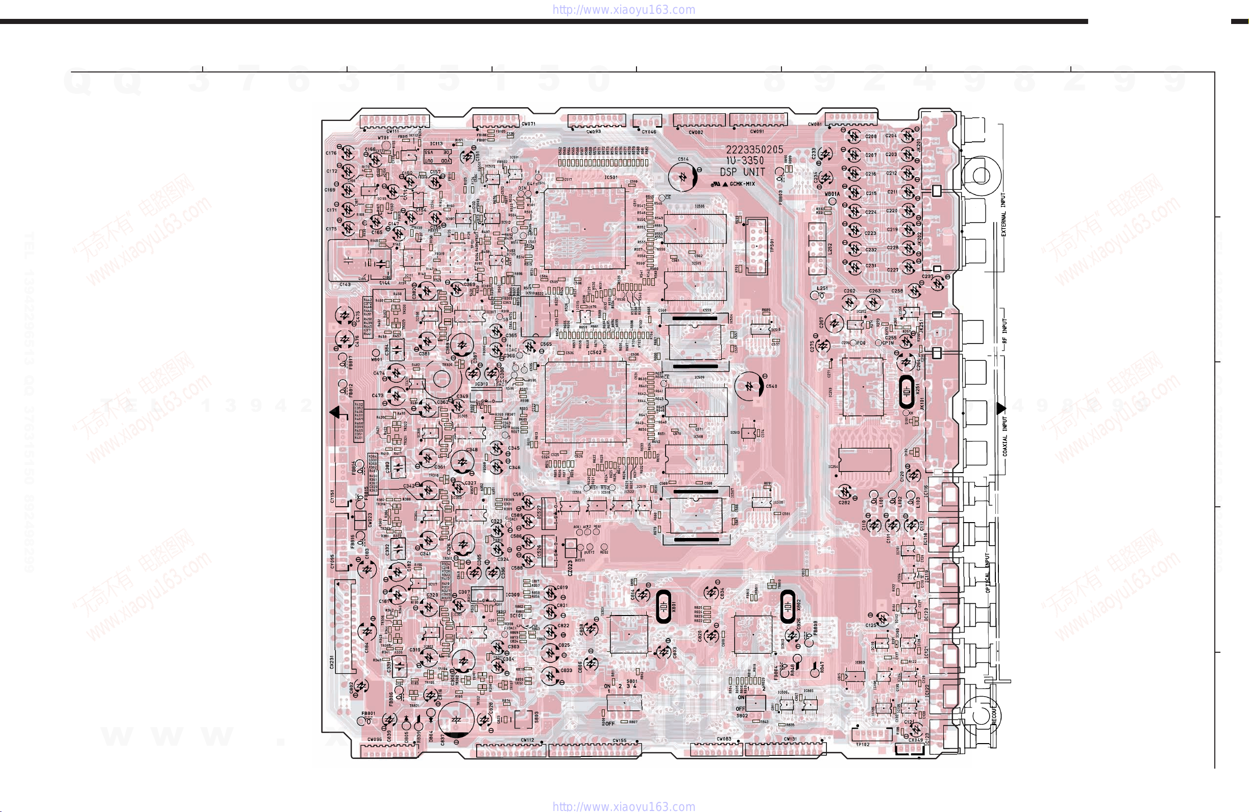
PRINTED WIRING BOARDS
1
AVR-4802/AVC-A11SR
2
3
4
5
76
8
Q
1U-3350 DSP UNIT Ass'y
Q
3
7
6
3
1 11
4
5 8
TEL 13942296513 QQ 376315150 892498299
T
E
L
1
3
9
4
2
2
9
15
1
6
1
8
9
48
1
12
13
BE
C
C
E
B
5
BE
C
C
B E
5
1
16
16
1
9
8
37
36
24
8
9
1
1 7 1 9 1 8
8
14
1
7
1
1
16
1
3
8
9
16
1
7
8
14
5
4
5
8
14
7
1
1
52
53
0
157208
156
50
1
105
104
50
8
1
91 4
9
1 8
2
4
9
8
2
9
9
A
26
1132
25
26
14
TEL 13942296513 QQ 376315150 892498299
B
8
75
0
51
16
5
4
1
9
9
2
8
9
4
2
9
8
C
Q
1
1
25
50
3
1
50
7
25
10
50
26
26
6
25
26
1
20
11
5
1
3
7
1
8
14
4
5
1
1
30
31 50
30
1
8
76100
5
14
558
4
1
8
1
4
1
3
58
4
1
15 28
E
C
B
14
15 28
1
1
14
1
8
7
157208
156
Q
1
52
53
105
104
w
w
w
.
1
9
1
x
E
C
B
20
20
20
14
BE
C
C
B E
1
2
BE
C
C
B E
22
23
58
4
1
58
4
1
58
4
1
E
E
C
C
B
B
BE
C
15 28
E
C
B
14
15 28
E
C
B
1
1
BE
C
E
C
BE
B
C
11
10
1
1
11
11
10
1
10
50
51
75
76
1
14
8
1
7
1
25
26
25
1
100
25
10
50
26
50
51
75
76
1
20
11
C
E
B
26
25
1
100
14
814
1 7
1 7
1
20
1
8
5
1
7
1
14
8
7
1
14
8
9
1
18
10
7
1
8
1
16
14
9
8
9
7
1
11
8
10
9
10
1
14
18
10
9
1
1
18
18
10
D
E
1
i
a
19
o
y
u
111 115 18 1
1
6
3
.
13
c
o
6
m
14
COMPONENT SIDE
26
Page 27
AVR-4802/AVC-A11SR
1
Q
1U-3350 DSP UNIT Ass'y
Q
3
7
2
6
3
TEL 13942296513 QQ 376315150 892498299
1
4
5
4
0
3
5
1
1
5
8
9
2
4
9
76
8
2
9
8
9
A
5 8
1
4
5 8
E
E
C
C
B
1
4
B
TEL 13942296513 QQ 376315150 892498299
5 8
1
4
5 8
B
C
C
C
E
E
B
E
B
C
E
B
E
E
C
C
B
B
BE
20
1
11
10
B
C
E
B
E
C
E
B
C
E
B
C
E
B
C
C
E
B
C
B
T
E
w
L
w
1
3
w
9
4
.
2
2
x
9
6
i
5
a
1
3
o
20
1
y
11
10
u
B
E
C
1
Q
Q
BE
C
6
CBEC
B
E
C
3
BE
C
BE
7
3
6
3
E
B
C
B
E
E
B
C
B
E
C
E
C
BE
E
B
C
E
C
B
E
C
B
E
C
B
B
C
E
E
C
B
E
C
B
B
C
E
E
C
B
E
C
E
C
B
B
B
C
E
B
E
B
C
B
E
C
E
B
BE
C
C
E
B
C
BE
C
C
E
B
C
BE
C
C
E
B
C
E
C
B
0
5
1
5
1
8
C
D
9
9
2
8
9
4
2
9
E
.
c
o
m
FOIL SIDE
27
Page 28
AVR-4802/AVC-A11SR
1
Q
1U-3351 AUDIO UNIT Ass'y
Q
3
7
2
6
BE
C
C
E
B
4
3
BE
C
C
E
B
1
8
1 4
5
TEL 13942296513 QQ 376315150 892498299
5
8
1
28
1
B
C
E
B
C
E
5
14
15
4
15 1
0
11
1
4
4
1
1
4
5
5
8
28
5
8
3
5
15
B
C
E
8
9
B
C
E
B
B
C
E
E
1
16
B
B
C
E
E
1
1
14
C
C
5
8
1
B
E
C
C
E
B
4
1
5
8
C
C
E
B
8
B
E
B
E
4
1
1
5
8
C
9
11
1
2
4
9
1
9
1
12
4
14
16
9
1
7
4
1
5
8
4
1
5
8
4
1
78
5
8
1
4
1
89
5
8
4
1
1
5
8
76
8
2
9
8
9
A
TEL 13942296513 QQ 376315150 892498299
B
T
E
L
1
3
9
4
4
1
5
8
4
1
2
2
9
6
5
1
3
5
8
4
1
5
8
4
1
5
8
4
1
5
8
4
1
5
8
4
1
5
8
4
1
5
8
1
1
4
1
4
1
5
5
8
8
4
2242
21
2242
21
1
5
8
14
15
1
28
Q
3
8
7
9
6
3
4
1
5
8
5
1
5
1
8
5
1
4
0
1
8
89
9
2
4
9
8
2
9
9
4
1
5
8
18
4
1
5
8
1
Q
C
1
16
14
15
14
15
21
1
4
1
5
8
28
1
4
1
5
8
28
1
18
4
1
5
8
1
4
1
4
1
5
5
8
8
9
8
4
5
B
C
1
E
B
C
8
E
4
1
5
8
4
1
5
8
C
E
B
11
89
1
16
89
1
16
89
1
16
D
78
w
w
w
.
4
1
5
8
4
1
x
5
8
13 5
i
a
1
o
15
y
22
u
1
1
42
15
6
3
1
.
c
15
1
o
11
14
4
1
1
8
5
4
1
m
1
E
4
COMPONENT SIDE
28
Page 29
AVR-4802/AVC-A11SR
1
Q
1U-3351 AUDIO UNIT Ass'y
TEL 13942296513 QQ 376315150 892498299
Q
3
7
2
6
3
1
5
4
0
3
5
1
5
8
9
2
4
9
76
8
2
9
8
9
A
TEL 13942296513 QQ 376315150 892498299
B
T
E
L
1
3
9
4
2
2
9
6
5
1
3
Q
Q
C
B E
3
0
5
1
5
1
3
6
7
8
C
D
9
9
2
8
9
4
2
9
w
w
w
.
x
i
a
o
y
u
1
6
3
.
c
o
E
m
FOIL SIDE
29
Page 30
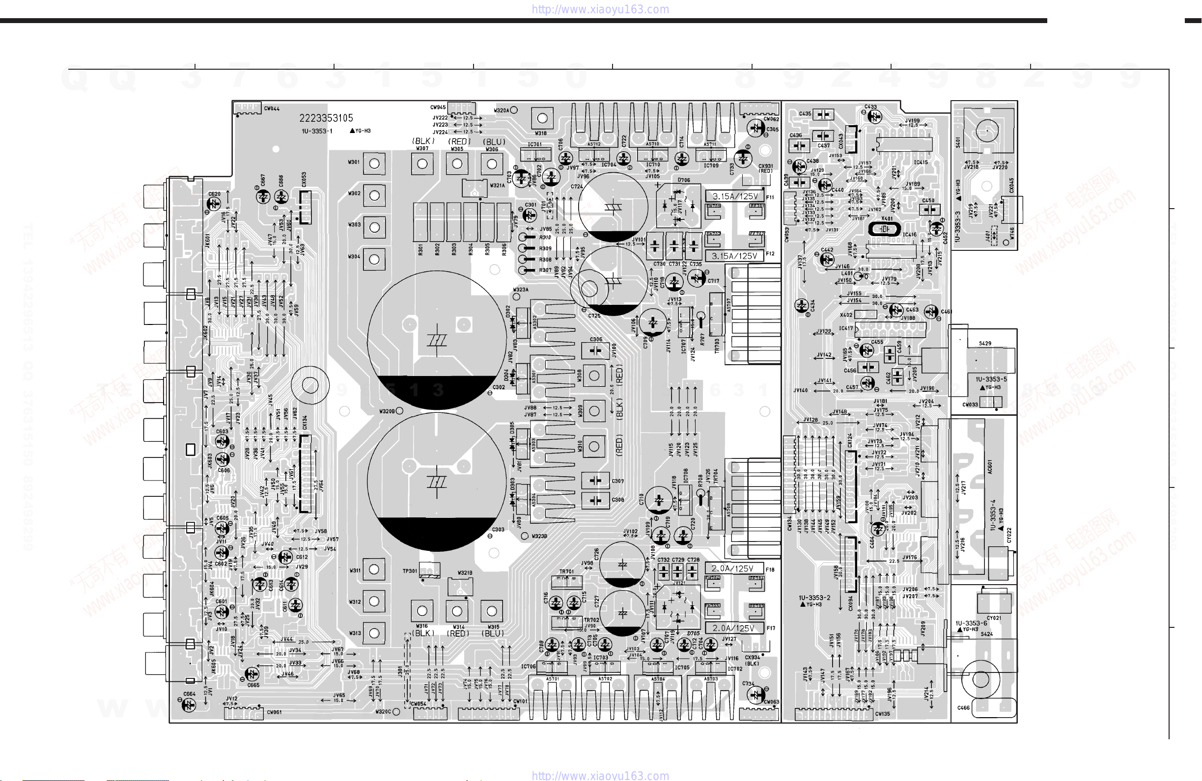
AVR-4802/AVC-A11SR
1
Q
1U-3353 PRIMARY UNIT Ass'y
TEL 13942296513 QQ 376315150 892498299
Q
3
7
2
6
4
1
3
5
1
1
5
4
0
3
5
1
5
8
1 6
9
1 5
2
4
14
1 8
20
1
1 8
9
11
10
916
76
8
916
2
14
9
8
9
A
TEL 13942296513 QQ 376315150 892498299
B
T
E
L
1
3
9
4
2
2
9
6
5
1
3
13
1
Q
Q
3
7
6
3
1
5
1
1 13
5
0
19 112
8
9
2
4
3
1 2
9
1
1 2
8
2
9
9
C
D
w
w
w
E
6
1
.
x
i
a
15
o
y
110
u
1
6
3
.
6
1
c
13
o
1
m
COMPONENT SIDE
30
Page 31

AVR-4802/AVC-A11SR
1
Q
1U-3353 PRIMARY UNIT Ass'y
TEL 13942296513 QQ 376315150 892498299
Q
3
7
2
6
BE
BE
C
C
3
BE
C
1
B
E
E
C
B
5
4
0
3
5
C
1
5
8
9
2
4
9
76
1 8
8
916
916
2
9
8
9
A
TEL 13942296513 QQ 376315150 892498299
B
T
E
L
1
3
9
4
B
C
E
B
C
E
B
C
E
B
C
E
9 16
9 16
9 16
2
1 8
2
9
6
5
1
3
B
E
B
E
B
E
B
E
B
E
18
18
18
BE
C
C
C
C
C
C
Q
B
C
E
E
C
B
B
C
E
Q
3
7
6
3
1
5
1
5
0
C
B
C
E
E
B
8 14
C
8
1 7
14
5 8
BE
17
9
2
5 8
814
5 8
5 8
9
4
14
14
14
8
2
9
9
C
D
w
w
w
.
x
i
a
o
y
u
1
6
3
.
c
o
E
m
FOIL SIDE
31
Page 32

AVR-4802/AVC-A11SR
1
Q
1U-3354 CONNECT UNIT Ass'y
TEL 13942296513 QQ 376315150 892498299
Q
3
7
2
6
3
16
17
6
1
1
3
5
1 113 1 15
8
4
1
1
1
4
5
15
1 11
17
115 10
0
5
1 1
1 11
8
1 4
911
1 4
9
16
1 4
1 4
2
4
23
22
9
76
8
1
2
2
9
8
9
A
TEL 13942296513 QQ 376315150 892498299
B
T
E
L
1
3
9
4
2
1 4
1
15
2
17
14
4
9
6
5
1
3
17
19
113
17
4
1
4
1
1
4
115
Q
Q
3
115 1
7
6
15
15
3
1
1 6
5
1
5
0
8
1 5
9
2
4
9
15
8
2
9
9
C
D
w
w
w
.
x
i
a
o
y
1919 1818
u
1
15
6
3
.
111
c
o
m
COMPONENT SIDE
E
32
Page 33
AVR-4802/AVC-A11SR
1
Q
1U-3354 CONNECT UNIT Ass'y
Q
3
7
2
6
11
110
20
3
TEL 13942296513 QQ 376315150 892498299
14
8
5
1
5
4
0
3
5
1
5
8
9
2
4
9
76
8
2
9
8
9
A
TEL 13942296513 QQ 376315150 892498299
E
C
B
C
E
B
E
C
B
B
T
E
L
1
3
45
9
4
2
2
9
6
5
1
3
B
C
E
B
C
E
9
16
8
1
14
46
60
1
15
31
30
16
B
B
C
C
E
E
B
B
C
C
E
E
Q
Q
3
7
6
B
B
C
C
E
E
3
1
5
1
BE
C
5
0
E
C
B
E
C
B
E
C
B
E
C
B
E
C
B
E
C
B
E
C
B
E
C
B
BE
C
E
C
B
E
C
B
8
B
C
E
B
C
E
B
C
E
B
C
E
B
C
E
B
C
E
B
C
E
B
C
E
BE
C
9
2
4
9
8
2
9
9
C
D
w
w
w
.
x
8
5
E
i
a
o
y
u
1
6
3
.
c
o
m
FOIL SIDE
33
Page 34

AVR-4802/AVC-A11SR
1
Q
1U-3355 REG. UNIT Ass'y
TEL 13942296513 QQ 376315150 892498299
Q
3
7
2
6
2
1
3
1
5
4
0
2
1
3
1
3
1
4
1
3
5
1
5
8
7
1
9
1 7
2
4
1 4
1 4
9
76
8
2
9
8
9
A
TEL 13942296513 QQ 376315150 892498299
B
T
E
w
L
w
1
3
w
9
4
.
2
2
x
9
6
i
5
a
1
3
3 3
o
11
y
1 15
9
1
u
1
2
1
2
1
2
1
3
1
3
1
2
1
Q
Q
6
3
7
3
6
.
3
1
5
4
c
0
5
1
1
o
m
8
C
1
3
3
1
1
5
D
E
9
9
2
8
9
4
2
9
COMPONENT SIDE
34
Page 35
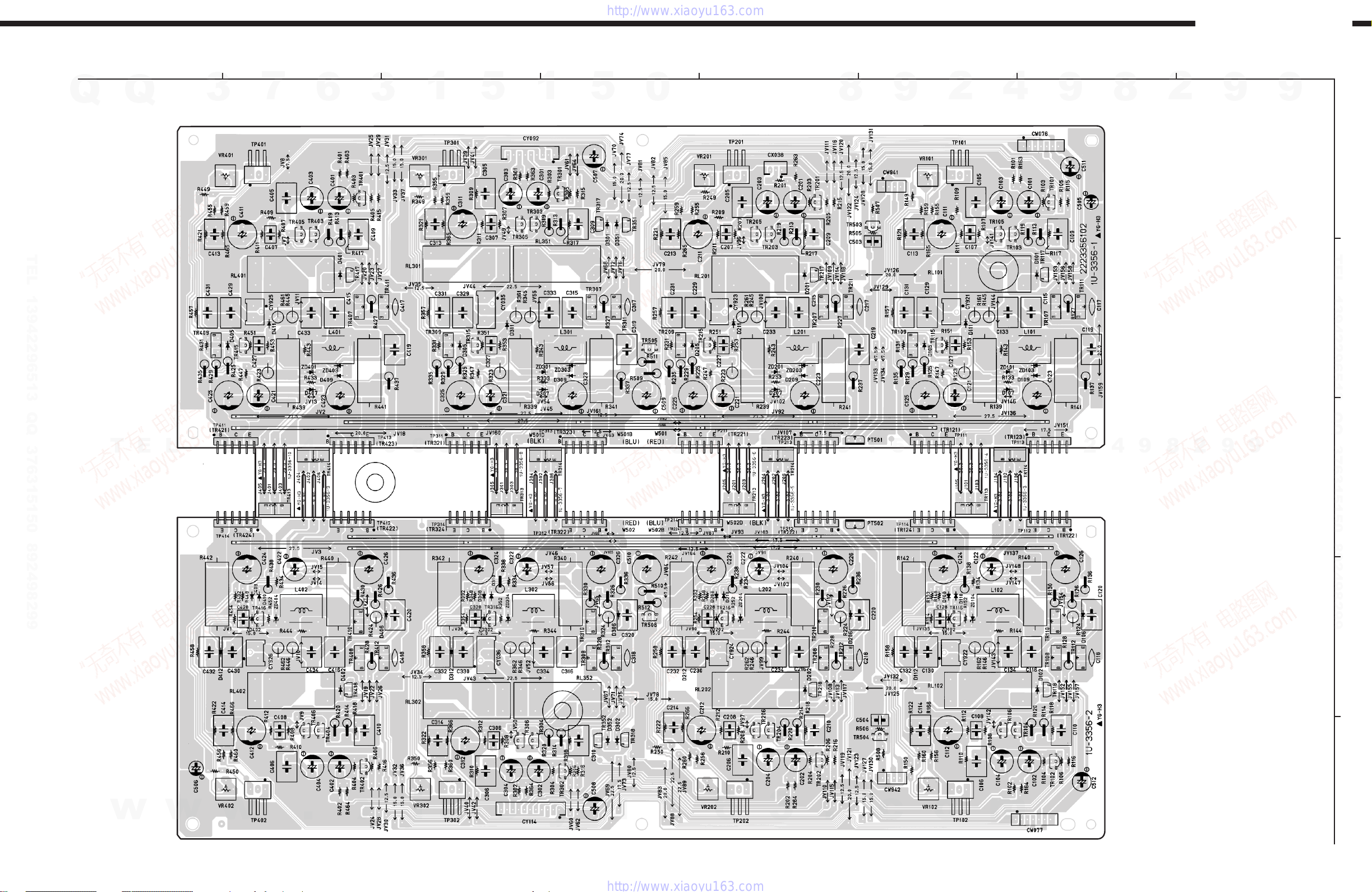
AVR-4802/AVC-A11SR
1
Q
1U-3356 AMP UNIT Ass'y
TEL 13942296513 QQ 376315150 892498299
Q
3
7
1 3
2
6
3
1
5
4
0
1 3
3
5
1
3
1
19
5
1 3
8
9
1 4
2
1 3
4
1 7
9
76
8
2
9
8
9
A
TEL 13942296513 QQ 376315150 892498299
B
T
E
w
L
w
1
3
w
9
4
2
2
9
6
5
1
3
a
13
111
o
y
u
1
13
.
x
i
Q
Q
6
3
13
3
7
6
.
3
1
1 4
c
5
1
o
5
0
13
m
8
1
7
9
2
4
9
8
2
9
9
C
D
E
COMPONENT SIDE
35
Page 36
Q
NOTE FOR PARTS LIST
l Part indicated with the mark "" are not always in stock and possibly to take a long period of time for supplying, or in
some case supplying of part may be refused.
7
Q
3
l When ordering of part, clearly indicate "1" and "I" (i) to avoid mis-supplying.
l Ordering part without stating its part number can not be supplied.
l Part indicated with the mark " " is not illustrated in the exploded view.
l Not including Carbon Film ±5%, 1/4W Type in the P.W.Board parts list. (Refer to the Schematic Diagram for those parts.)
WARNING:
Parts marked with this symbol
Use ONLY replacement parts recommended by the manufacturer.
6
3
1
5
1
5
0
have critical characteristics.
8
9
2
AVR-4802/AVC-A11SR
4
9
8
2
9
9
ll
l Resistors
ll
TEL 13942296513 QQ 376315150 892498299
Ex.: RN 14K 2E 182 G FR
Type Shape Power Resist- Allowable Others
and per- ance error
formance
t
RD : Carbon 2B : 1/8W F : ±1% P : Pulse-resistant type
RC : Composition 2E : 1/4W G :±2% NL : Low noise type
RS : Metal oxide film 2H : 1/2W J : ±5% NB : Non-burning type
RW : Winding 3A : 1W K : ±10% FR : Fuse-resistor
RN : Metal film 3D : 2W M : ±20% F : Lead wire forming
RK : Metal mixture 3F : 3W
Resistance
1 8 2 ⇒ 1800 ohm = 1.8 kohm
s
s
• Units: ohm
1 R 2 ⇒ 1.2 ohm
s
s
• Units: ohm
TEL
13942296513
t
3H : 5W
Indicates number of zeros after effective number.
2-digit effective number.
1-digit effective number.
2-digit effective number, decimal point indicated by R.
t
t
ll
l Capacitors
ll
Ex.: CE 04W 1H 2R2 M BP
Type Shape Dielectric Capacity Allowable Others
t
CE : Aluminum foil 0J : 6.3V F : ±1% HS : High stability type
electrolytic
CA : Aluminum solid 1A : 10V G : ±2% BP : Non-polar type
electrolytic
CS : Tantalum electrolytic 1C : 16V J : ±5% HR : Ripple-resistant type
CQ : Film 1E : 25V K : ±10% DL : For change and discharge
CK : Ceramic 1V : 35V M : ±20% HF : For assuring high
CC : Ceramic 1H : 50V Z : +80% U : UL part
CP : Oil 2A : 100V –20% C : CSA part
CM : Mica 2B : 125V P : +100% W : UL-CSA type
CF : Metallized 2C : 160V –0% F : Lead wire forming
CH : Metallized 2D : 200V C : ±0.25pF
Capacity (electrolyte only)
2 2 2 ⇒ 2200µF
s
s
7
3
Q
Q
• Units: µF.
2 R 2 ⇒ 2.2µF
s
s
• Units: µF.
Capacity (except electrolyte)
2 2 2 ⇒ 2200pF=0.0022µF
s
s
• Units: pF.
2 2 1 ⇒ 220pF
s
s
• Units: pF.
• When the dielectric strength is indicated in AC, "AC" is included after the dieelectric
strength value.
and per- strength error
formance
1
5
t
0
t
2E : 250V D : ±0.5pF
2H : 500V = : Others
2J : 630V
Indicates number of zeros after effective number.
2-digit effective number.
5
1
3
6
1-digit effective number.
2-digit effective number, decimal point indicated by R.
(More than 2) Indicates number of zeros after effective number.
(0 or 1) Indicates number of zeros after effective number.
2-digit effective number.
2-digit effective number.
8
requency
9
t
2
4
9
8
2
9
TEL 13942296513 QQ 376315150 892498299
9
w
w
w
.
xia
o
y
u
1
6
3
.
c
o
m
36
Page 37

PARTS LIST OF P.W.B. UNIT
1U-3350 DSP UNIT ASS'Y
Q
Q
Ref. No. Part No. Part Name Remarks
SEMICONDUCTORS GROUP
IC101 262 2572 901 IC SN74LVU04APW-EL2
IC102-104 262 2944 908 IC SN74HC151APW-EL2
IC105 262 2945 907 IC SN74HC153APW-EL2
IC106 262 2861 900 IC 74VHC123AMTCX
IC107 262 2870 904 IC 74LVX157MTC
IC108 262 2519 906 IC SN74LV00APW-EL2
IC109 262 2980 904 IC SN74AHC1G04DBV
IC110 262 2557 900 IC SN74LV14APW-EL2
TEL 13942296513 QQ 376315150 892498299
IC111 262 2675 015 IC LC89055W-RA8
IC112 262 2781 909 IC SN74LV4040APW
IC113 399 0575 008 Crystal 12.287 MHz
IC114 262 2772 905 IC AK5353
IC115 263 0934 900 IC BA4510F-E2
IC116 269 0178 007 Optical connector GP1F37R1
IC117 263 0896 909 IC NJM2068MD-T1
IC118-121 269 0178 007 Optical connector GP1F37R1
IC122,123 269 0177 008 Optical connector GP1F38T2
IC124 262 2557 900 IC SN74LV14APW-EL2
IC125 262 2517 908 IC SN74LV08APW-EL2
IC201-204 263 0896 909 IC NJM2068MD-T1
IC301 262 2768 906 IC AD1854KRSRL
TEL
IC302 263 0896 909 IC NJM2068MD-T1
IC303 262 2768 906 IC AD1854KRSRL
IC304 263 0896 909 IC NJM2068MD-T1
IC305 262 2768 906 IC AD1854KRSRL
IC306 263 0896 909 IC NJM2068MD-T1
IC307 262 2768 906 IC AD1854KRSRL
IC308 263 0896 909 IC NJM2068MD-T1
IC309,310 263 1100 005 IC KIA7805API
IC471 263 0896 909 IC NJM2068MD-T1
IC501,502 262 2853 002 IC ADSP-21065L
IC504 GEN5216 DSP1 CPU SUB ASS'Y AVR MODEL ONLY
IC505,506 262 2855 000 IC 16M SDRAM TSOP-8 H/W
IC507 GEN5217 DSP2 CPU SUB ASS'Y AVR MODEL ONLY
IC508,509 262 2855 000 IC 16M SDRAM TSOP-8 H/W
IC510 262 2854 904 IC HG-8002JA33MHZPCCX
IC511 262 2519 906 IC SN74LV00APW-EL2
w
w
IC512 262 2781 909 IC SN74LV4040APW
IC513 262 2519 906 IC SN74LV00APW-EL2
3
7
6
3
1
5
1
5
13942296513
2622779005
LH28F800BVE-BTL90
GEN5300 DSP1 CPU SUB ASS'Y 2 AVC MODEL ONLY
2622779005
LH28F800BVE-BTL90
2622779005
LH28F800BVE-BTL90
GEN5301 DSP2 CPU SUB ASS'Y 2 AVC MODEL ONLY
2622779005
LH28F800BVE-BTL90
w
.
xia
o
y
u
0
Q
Q
1
Ref. No. Part No. Part Name Remarks
IC514 262 2780 900 IC SN74AHCT541PW
IC515 262 2729 903 IC SN74LV02APW-EL2
IC516 262 2606 903 IC SN74AHCT573PW
IC517 262 2682 901 IC SN74LV573ANS-EL2
IC518 262 2641 900 IC SN74LV541APW
IC519 262 2729 903 IC SN74LV02APW-EL2
IC520 262 2606 903 IC SN74AHCT573PW
IC521 262 2682 901 IC SN74LV573ANS-EL2
IC522 262 2641 900 IC SN74LV541APW
IC523 262 2948 904 IC SN74LV86APW
IC526,527 263 1048 002 IC BA033T
IC801 GEN5215 SUB CPU ASS'Y AVR MODEL ONLY
IC802 GEN5214 MAIN CPU SUB ASS'Y AVR MODEL ONLY
IC803 262 2641 900 IC SN74LV541APW
IC805 262 2785 905 IC SN74LV125APW
7
3
IC806 262 2786 904 IC SN74LV126APW
TR102,103 269 0192 902
TR104,105 269 0184 907 Transistor KRA102S-RTK
TR107,108 273 0460 905 Transistor KTC2875B-RTK
TR301-303 269 0184 907 Transistor KRA102S-RTK
TR305-308 273 0460 905 Transistor KTC2875B-RTK
TR309-311 269 0184 907 Transistor KRA102S-RTK
TR313-316 273 0460 905 Transistor KTC2875B-RTK
TR317-319 269 0184 907 Transistor KRA102S-RTK
TR321-324 273 0460 905 Transistor KTC2875B-RTK
TR325-327 269 0184 907 Transistor KRA102S-RTK
TR329-332 273 0460 905 Transistor KTC2875B-RTK
TR471,472 273 0460 905 Transistor KTC2875B-RTK
TR501,502 269 0184 907 Transistor KRA102S-RTK
TR801 269 0192 902
TR802 271 0299 905 Transistor 2SA1505Y-RTK
TR803 269 0192 902
TR804 269 0184 907 Transistor KRA102S-RTK
TR806 269 0192 902
TR807 269 0184 907 Transistor KRA102S-RTK
TR808 269 0193 901
6
3
TR809 273 0384 900 Transistor 2SC2412KT96(S)
TR810 269 0192 902
AVR-4802/AVC-A11SR
4
2
9
8
GEN5299 SUB CPU ASS'Y 2 AVC MODEL ONLY
GEN5298 MAIN CPU SUB ASS'Y 2 AVC MODEL ONLY
0
5
1
5
1
3
6
Transistor KRC102S-RTK(10K-10K)
Transistor KRC102S-RTK(10K-10K)
Transistor KRC102S-RTK(10K-10K)
Transistor KRC102S-RTK(10K-10K)
Transistor KRC104S-RTK(47K-47K)
.
c
o
Transistor KRC102S-RTK(10K-10K)
9
9
8
m
2
8
4
2
262 2784 003
TMP95FY64F
2622784003
TMP95FY64F
262 2784 003
TMP95FY64F
262 2784 003
TMP95FY64F
2
8
9
9
9
9
TEL 13942296513 QQ 376315150 892498299
9
37
Page 38

AVR-4802/AVC-A11SR
7
Q
Q
TEL 13942296513 QQ 376315150 892498299
TEL
w
3
Ref. No. Part No. Part Name Remarks Ref. No. Part No. Part Name Remarks
TR812,813 273 0384 900 Transistor 2SC2412KT96(S)
TR814 271 0238 908 Transistor 2SA1037KT96(S/R)
TR815 273 0384 900 Transistor 2SC2412KT96(S)
TR816 274 0163 904 Transistor 2SD601A
TR817 273 0384 900 Transistor 2SC2412KT96(S)
TR818 271 0238 908 Transistor 2SA1037KT96(S/R)
TR819 273 0384 900 Transistor 2SC2412KT96(S)
TR820,821 269 0193 901
TR822 269 0184 907 Transistor KRA102S-RTK
TR823 269 0193 901
D101,102 276 0739 907 Diode KDS181-RTK(A-COM)
D301-304 276 0740 909 Diode KDS184-RTK(K-COM)
D802,803 276 0739 907 Diode KDS181-RTK(A-COM)
D804,805 276 0704 903 Diode 1SR35-400A(T93X)
ZD801 276 0693 946 Zener diode UDZ3.0B
SC101 279 0016 904 Thyristor SF0R1A42(TPE2)
RESISTORS GROUP
R101-106 247 2005 945 Carbon chip 150 ohm 1/16W RM73B--151JT
13942296513
R107-109 247 2005 903 Carbon chip 100 ohm 1/16W RM73B--101JT
R110-114 247 2009 909 Carbon chip 4.7 kohm 1/16W
R115 247 2008 926 Carbon chip 2.2 kohm 1/16W RM73B--222JT
R116,117 247 2011 942 Carbon chip 47 kohm 1/16W RM73B--473JT
R118 247 2008 926 Carbon chip 2.2 kohm 1/16W RM73B--222JT
R119 247 2011 942 Carbon chip 47 kohm 1/16W RM73B--473JT
R120 247 2008 926 Carbon chip 2.2 kohm 1/16W RM73B--222JT
R122 247 2005 903 Carbon chip 100 ohm 1/16W RM73B--101JT
R123 247 2014 965 Carbon chip 1 Mohm 1/16W RM73B--105JT
R124-126 247 2005 903 Carbon chip 100 ohm 1/16W RM73B--101JT
R127 247 2011 900 Carbon chip 33 kohm 1/16W RM73B--333JT
R128 247 2003 989 Carbon chip 33 ohm 1/16W RM73B--330JT
R129,130 247 2018 903 Carbon chip 0 ohm 1/16W RM73B--0R0KT
R131,132 247 2005 903 Carbon chip 100 ohm 1/16W RM73B--101JT
R134 247 2005 903 Carbon chip 100 ohm 1/16W RM73B--101JT
R135 247 2018 903 Carbon chip 0 ohm 1/16W RM73B--0R0KT
R138 247 2009 983 Carbon chip 10 kohm 1/16W RM73B--103JT
R142 247 2018 903 Carbon chip 0 ohm 1/16W RM73B--0R0KT
R143 247 2009 967 Carbon chip 8.2 kohm 1/16W RM73B--822JT
R144 247 2008 955 Carbon chip 3 kohm 1/16W RM73B--302JT
R145 247 2009 912 Carbon chip 5.1 kohm 1/16W RM73B--512JT
R146 247 2004 975 Carbon chip 75 ohm 1/16W RM73B--750JT
R147-149 247 2003 989 Carbon chip 33 ohm 1/16W RM73B--330JT
R150 247 2005 903 Carbon chip 100 ohm 1/16W RM73B--101JT
R151-154 247 2018 903 Carbon chip 0 ohm 1/16W RM73B--0R0KT
R155-162 247 2005 903 Carbon chip 100 ohm 1/16W RM73B--101JT
w
w
R163,164 247 2009 983 Carbon chip 10 kohm 1/16W RM73B--103JT
R167,168 247 2006 960 Carbon chip 470 ohm 1/16W RM73B--471JT
6
Transistor KRC104S-RTK(47K-47K)
Transistor KRC104S-RTK(47K-47K)
.
xia
3
1
5
o
1
5
0
Q
RM73B--472JT (1608)
y
u
1
R169,170 247 2009 938 Carbon chip 6.2 kohm 1/16W RM73B--622JT
R171,172 247 2010 901 Carbon chip 12 kohm 1/16W RM73B--123JT
R175-178 247 2009 909 Carbon chip 4.7 kohm 1/16W
R179,180 247 2011 942 Carbon chip 47 kohm 1/16W RM73B--473JT
R183 247 2007 943 Carbon chip 1 kohm 1/16W RM73B--102JT
R184 247 2011 942 Carbon chip 47 kohm 1/16W RM73B--473JT
R185,186 247 2018 903 Carbon chip 0 ohm 1/16W RM73B--0R0KT
R187,188 247 2006 902 Carbon chip 330 ohm 1/16W
R189,190 247 2007 969 Carbon chip 1.2 kohm 1/16W RM73B--122JT
R191,192 247 2005 903 Carbon chip 100 ohm 1/16W RM73B--101JT
R195,196 247 2007 943 Carbon chip 1 kohm 1/16W RM73B--102JT
R197 247 2003 989 Carbon chip 33 ohm 1/16W RM73B--330JT
R198 247 2005 903 Carbon chip 100 ohm 1/16W RM73B--101JT
R199-204 247 2012 925 Carbon chip 100 kohm 1/16W RM73B--104JT
R205,206 247 2005 903 Carbon chip 100 ohm 1/16W RM73B--101JT
R207,208 247 2004 920 Carbon chip 47 ohm 1/16W RM73B--470JT
R209,210 247 2011 942 Carbon chip 47 kohm 1/16W RM73B--473JT
R211 247 2012 925 Carbon chip 100 kohm 1/16W RM73B--104JT
R212 247 2010 985 Carbon chip 27 kohm 1/16W RM73B--273JT
R213 247 2012 925 Carbon chip 100 kohm 1/16W RM73B--104JT
R214 247 2013 982 Carbon chip 470 kohm 1/16W RM73B--474JT
R215,216 247 2005 903 Carbon chip 100 ohm 1/16W RM73B--101JT
R217,218 247 2004 920 Carbon chip 47 ohm 1/16W RM73B--470JT
7
3
Q
R219,220 247 2011 942 Carbon chip 47 kohm 1/16W RM73B--473JT
R221-224 247 2012 925 Carbon chip 100 kohm 1/16W RM73B--104JT
R225,226 247 2005 903 Carbon chip 100 ohm 1/16W RM73B--101JT
R227,228 247 2004 920 Carbon chip 47 ohm 1/16W RM73B--470JT
R229,230 247 2011 942 Carbon chip 47 kohm 1/16W RM73B--473JT
R231-234 247 2012 925 Carbon chip 100 kohm 1/16W RM73B--104JT
R235,236 247 2005 903 Carbon chip 100 ohm 1/16W RM73B--101JT
R237,238 247 2004 920 Carbon chip 47 ohm 1/16W RM73B--470JT
R239,240 247 2011 942 Carbon chip 47 kohm 1/16W RM73B--473JT
R241 247 2010 956 Carbon chip 20 kohm 1/16W RM73B--203JT
R242-247 247 2018 903 Carbon chip 0 ohm 1/16W RM73B--0R0KT
R250 247 2018 903 Carbon chip 0 ohm 1/16W RM73B--0R0KT
R308-310 247 2018 903 Carbon chip 0 ohm 1/16W RM73B--0R0KT
R311-313 247 2009 983 Carbon chip 10 kohm 1/16W RM73B--103JT
R314-316 247 2018 903 Carbon chip 0 ohm 1/16W RM73B--0R0KT
R317 247 2009 983 Carbon chip 10 kohm 1/16W RM73B--103JT
R318 247 2018 903 Carbon chip 0 ohm 1/16W RM73B--0R0KT
R319-322 247 2008 900 Carbon chip 1.8 kohm 1/16W RM73B--182JT
R323-330 247 2008 913 Carbon chip 2 kohm 1/16W RM73B--202JT
R333,334 247 2005 974 Carbon chip 200 ohm 1/16W RM73B--201JT
R337,338 247 2012 925 Carbon chip 100 kohm 1/16W RM73B--104JT
R339,340 247 2007 914 Carbon chip 750 ohm 1/16W RM73B--751JT
R341,342 247 2005 974 Carbon chip 200 ohm 1/16W RM73B--201JT
R343-346 247 2011 900 Carbon chip 33 kohm 1/16W RM73B--333JT
R347 247 2007 943 Carbon chip 1 kohm 1/16W RM73B--102JT
R348 247 2011 942 Carbon chip 47 kohm 1/16W RM73B--473JT
6
3
R351-353 247 2009 983 Carbon chip 10 kohm 1/16W RM73B--103JT
6
8
3
.
9
1
1
5
c
2
5
o
4
0
m
9
8
9
8
2
2
9
RM73B--472JT (1608)
RM73B--331JT (1608)
2
8
9
4
9
9
TEL 13942296513 QQ 376315150 892498299
9
38
Page 39

AVR-4802/AVC-A11SR
7
Q
Q
TEL 13942296513 QQ 376315150 892498299
TEL
w
3
Ref. No. Part No. Part Name Remarks Ref. No. Part No. Part Name Remarks
R354-356 247 2018 903 Carbon chip 0 ohm 1/16W RM73B--0R0KT
R357 247 2009 983 Carbon chip 10 kohm 1/16W RM73B--103JT
R359 247 2008 900 Carbon chip 1.8 kohm 1/16W RM73B--182JT
R360 247 2008 942 Carbon chip 2.7 kohm 1/16W RM73B--272JT
R361 247 2008 900 Carbon chip 1.8 kohm 1/16W RM73B--182JT
R362 247 2008 942 Carbon chip 2.7 kohm 1/16W RM73B--272JT
R363 247 2008 913 Carbon chip 2 kohm 1/16W RM73B--202JT
R364 247 2010 914 Carbon chip 13 kohm 1/16W RM73B--133JT
R365 247 2008 913 Carbon chip 2 kohm 1/16W RM73B--202JT
R366 247 2008 926 Carbon chip 2.2 kohm 1/16W RM73B--222JT
R367 247 2008 913 Carbon chip 2 kohm 1/16W RM73B--202JT
R368 247 2008 926 Carbon chip 2.2 kohm 1/16W RM73B--222JT
R369 247 2008 913 Carbon chip 2 kohm 1/16W RM73B--202JT
R370 247 2010 914 Carbon chip 13 kohm 1/16W RM73B--133JT
R373,374 247 2005 974 Carbon chip 200 ohm 1/16W RM73B--201JT
R375-377 247 2012 925 Carbon chip 100 kohm 1/16W RM73B--104JT
R378 247 2009 983 Carbon chip 10 kohm 1/16W RM73B--103JT
R379,380 247 2006 986 Carbon chip 560 ohm 1/16W RM73B--561JT
R381,382 247 2005 974 Carbon chip 200 ohm 1/16W RM73B--201JT
R383-386 247 2011 900 Carbon chip 33 kohm 1/16W RM73B--333JT
R387 247 2007 943 Carbon chip 1 kohm 1/16W RM73B--102JT
R388 247 2011 942 Carbon chip 47 kohm 1/16W RM73B--473JT
R390-392 247 2009 983 Carbon chip 10 kohm 1/16W RM73B--103JT
R393-395 247 2018 903 Carbon chip 0 ohm 1/16W RM73B--0R0KT
13942296513
R396 247 2009 983 Carbon chip 10 kohm 1/16W RM73B--103JT
R397-400 247 2008 900 Carbon chip 1.8 kohm 1/16W RM73B--182JT
R401-408 247 2008 913 Carbon chip 2 kohm 1/16W RM73B--202JT
R411,412 247 2005 974 Carbon chip 200 ohm 1/16W RM73B--201JT
R415,416 247 2012 925 Carbon chip 100 kohm 1/16W RM73B--104JT
R417,418 247 2007 914 Carbon chip 750 ohm 1/16W RM73B--751JT
R419,420 247 2005 974 Carbon chip 200 ohm 1/16W RM73B--201JT
R421-424 247 2011 900 Carbon chip 33 kohm 1/16W RM73B--333JT
R425 247 2007 943 Carbon chip 1 kohm 1/16W RM73B--102JT
R426 247 2011 942 Carbon chip 47 kohm 1/16W RM73B--473JT
R429-431 247 2009 983 Carbon chip 10 kohm 1/16W RM73B--103JT
R432-434 247 2018 903 Carbon chip 0 ohm 1/16W RM73B--0R0KT
R435 247 2009 983 Carbon chip 10 kohm 1/16W RM73B--103JT
R437-440 247 2008 900 Carbon chip 1.8 kohm 1/16W RM73B--182JT
R441-448 247 2008 913 Carbon chip 2 kohm 1/16W RM73B--202JT
R451,452 247 2005 974 Carbon chip 200 ohm 1/16W RM73B--201JT
R453-456 247 2012 925 Carbon chip 100 kohm 1/16W RM73B--104JT
R457,458 247 2006 986 Carbon chip 560 ohm 1/16W RM73B--561JT
R459,460 247 2005 974 Carbon chip 200 ohm 1/16W RM73B--201JT
R461-464 247 2011 900 Carbon chip 33 kohm 1/16W RM73B--333JT
R465 247 2007 943 Carbon chip 1 kohm 1/16W RM73B--102JT
R466 247 2011 942 Carbon chip 47 kohm 1/16W RM73B--473JT
R473,474 247 2006 957 Carbon chip 430 ohm 1/16W RM73B--431JT
R475,476 247 2007 969 Carbon chip 1.2 kohm 1/16W RM73B--122JT
R479,480 247 2007 985 Carbon chip 1.5 kohm 1/16W RM73B--152JT
R481,482 247 2006 999 Carbon chip 620 ohm 1/16W RM73B--621JT
w
w
R485,486 247 2012 925 Carbon chip 100 kohm 1/16W RM73B--104JT
6
.
xia
3
1
5
o
1
y
5
u
0
Q
Q
1
R493 247 2018 903 Carbon chip 0 ohm 1/16W
R496 247 2018 903 Carbon chip 0 ohm 1/16W
R498,499 247 2018 903 Carbon chip 0 ohm 1/16W
R501 247 2018 903 Carbon chip 0 ohm 1/16W
R502,503 247 2005 903 Carbon chip 100 ohm 1/16W RM73B--101JT
R505,506 247 2005 903 Carbon chip 100 ohm 1/16W RM73B--101JT
R507-511 247 2009 983 Carbon chip 10 kohm 1/16W RM73B--103JT
R512 247 2005 903 Carbon chip 100 ohm 1/16W RM73B--101JT
R513-515 247 2009 983 Carbon chip 10 kohm 1/16W RM73B--103JT
R516-521 247 2005 903 Carbon chip 100 ohm 1/16W RM73B--101JT
R522 247 2009 983 Carbon chip 10 kohm 1/16W RM73B--103JT
R523,524 247 2005 903 Carbon chip 100 ohm 1/16W RM73B--101JT
R525 247 2009 983 Carbon chip 10 kohm 1/16W RM73B--103JT
R526-543 247 2005 903 Carbon chip 100 ohm 1/16W RM73B--101JT
R544 247 2009 983 Carbon chip 10 kohm 1/16W RM73B--103JT
R545-582 247 2005 903 Carbon chip 100 ohm 1/16W RM73B--101JT
R583-594 247 2009 983 Carbon chip 10 kohm 1/16W RM73B--103JT
R595-598 247 2005 903 Carbon chip 100 ohm 1/16W RM73B--101JT
R599-603 247 2009 983 Carbon chip 10 kohm 1/16W RM73B--103JT
R604 247 2005 903 Carbon chip 100 ohm 1/16W RM73B--101JT
R605-607 247 2009 983 Carbon chip 10 kohm 1/16W RM73B--103JT
R608-613 247 2005 903 Carbon chip 100 ohm 1/16W RM73B--101JT
7
3
R614 247 2009 983 Carbon chip 10 kohm 1/16W RM73B--103JT
R615,616 247 2005 903 Carbon chip 100 ohm 1/16W RM73B--101JT
R617 247 2009 983 Carbon chip 10 kohm 1/16W RM73B--103JT
R618-635 247 2005 903 Carbon chip 100 ohm 1/16W RM73B--101JT
R636 247 2009 983 Carbon chip 10 kohm 1/16W RM73B--103JT
R637-661 247 2005 903 Carbon chip 100 ohm 1/16W RM73B--101JT
R662 247 2009 983 Carbon chip 10 kohm 1/16W RM73B--103JT
R665-670 247 2009 983 Carbon chip 10 kohm 1/16W RM73B--103JT
R671,672 247 2005 903 Carbon chip 100 ohm 1/16W RM73B--101JT
R673,674 247 2003 989 Carbon chip 33 ohm 1/16W RM73B--330JT
R675 247 2009 983 Carbon chip 10 kohm 1/16W RM73B--103JT
R676 247 2018 903 Carbon chip 0 ohm 1/16W
R677 247 2003 989 Carbon chip 33 ohm 1/16W RM73B--330JT
R678-683 247 2009 983 Carbon chip 10 kohm 1/16W RM73B--103JT
R684,685 247 2005 903 Carbon chip 100 ohm 1/16W RM73B--101JT
R688-691 247 2009 983 Carbon chip 10 kohm 1/16W RM73B--103JT
R692 247 2018 903 Carbon chip 0 ohm 1/16W
R693 247 2003 989 Carbon chip 33 ohm 1/16W RM73B--330JT
R694-698 247 2005 903 Carbon chip 100 ohm 1/16W RM73B--101JT
R700 247 2008 913 Carbon chip 2 kohm 1/16W RM73B--202JT
R701-704 247 2005 903 Carbon chip 100 ohm 1/16W RM73B--101JT
R705-707 247 2009 983 Carbon chip 10 kohm 1/16W RM73B--103JT
R801,802 247 2009 983 Carbon chip 10 kohm 1/16W RM73B--103JT
R804-807 247 2018 903 Carbon chip 0 ohm 1/16W RM73B--0R0KT
R808 247 2007 943 Carbon chip 1 kohm 1/16W RM73B--102JT
6
3
R809,810 247 2018 903 Carbon chip 0 ohm 1/16W RM73B--0R0KT
6
8
3
.
9
1
1
5
c
2
5
o
4
0
m
9
8
9
8
2
2
RM73B--0R0KT
RM73B--0R0KT
RM73B--0R0KT
RM73B--0R0KT
8
9
4
RM73B--0R0KT
RM73B--0R0KT
9
2
9
9
TEL 13942296513 QQ 376315150 892498299
9
39
Page 40

AVR-4802/AVC-A11SR
7
Q
Q
TEL 13942296513 QQ 376315150 892498299
TEL
w
3
Ref. No. Part No. Part Name Remarks Ref. No. Part No. Part Name Remarks
R811 247 2009 983 Carbon chip 10 kohm 1/16W RM73B--103JT
R814 247 2009 983 Carbon chip 10 kohm 1/16W RM73B--103JT
R815-817 247 2009 983 Carbon chip 10 kohm 1/16W RM73B--103JT
R818 247 2018 903 Carbon chip 0 ohm 1/16W RM73B--0R0KT
R819 247 2009 983 Carbon chip 10 kohm 1/16W RM73B--103JT
R820 247 2018 903 Carbon chip 0 ohm 1/16W RM73B--0R0KT
R822-825 247 2018 903 Carbon chip 0 ohm 1/16W RM73B--0R0KT
R827 247 2009 983 Carbon chip 10 kohm 1/16W RM73B--103JT
R828 247 2011 942 Carbon chip 47 kohm 1/16W RM73B--473JT
R829 247 2009 983 Carbon chip 10 kohm 1/16W RM73B--103JT
R831 247 2009 983 Carbon chip 10 kohm 1/16W RM73B--103JT
R832 247 2009 909 Carbon chip 4.7 kohm 1/16W
R833-835 247 2009 983 Carbon chip 10 kohm 1/16W RM73B--103JT
R837,838 247 2009 983 Carbon chip 10 kohm 1/16W RM73B--103JT
R839 241 2387 908 Carbon film 1 ohm 1/4W(NB) RD14B2E010JNBST
R840,841 247 2009 983 Carbon chip 10 kohm 1/16W RM73B--103JT
R843 247 2007 943 Carbon chip 1 kohm 1/16W RM73B--102JT
R844,845 247 2009 983 Carbon chip 10 kohm 1/16W RM73B--103JT
R846 247 2011 942 Carbon chip 47 kohm 1/16W RM73B--473JT
R847 247 2009 983 Carbon chip 10 kohm 1/16W RM73B--103JT
R849,850 247 2007 943 Carbon chip 1 kohm 1/16W RM73B--102JT
R851 247 2001 981 Carbon chip 4.7 ohm 1/16W RM73B--4R7KT
R852 247 2009 983 Carbon chip 10 kohm 1/16W RM73B--103JT
R853 247 2001 981 Carbon chip 10 kohm 1/16W RM73B--103JT
13942296513
R854 247 2012 925 Carbon chip 100 kohm 1/16W RM73B--104JT
R855 247 2009 983 Carbon chip 10 kohm 1/16W RM73B--103JT
R856 247 2005 903 Carbon chip 100 ohm 1/16W RM73B--101JT
R857 247 2007 985 Carbon chip 1.5 kohm 1/16W RM73B--152JT
R858 247 2011 942 Carbon chip 47 kohm 1/16W RM73B--473JT
R859 247 2012 925 Carbon chip 100 kohm 1/16W RM73B--104JT
R860 247 2005 903 Carbon chip 100 ohm 1/16W RM73B--101JT
R861 247 2013 908 Carbon chip 220 kohm 1/16W RM73B--224JT
R862 247 2011 942 Carbon chip 47 kohm 1/16W RM73B--473JT
R863 247 2004 920 Carbon chip 47 ohm 1/16W RM73B--470JT
R864 247 2007 943 Carbon chip 1 kohm 1/16W RM73B--102JT
R865 247 2018 903 Carbon chip 0 ohm 1/16W RM73B--0R0KT
R868 247 2009 909 Carbon chip 4.7 kohm 1/16W
R869 247 2001 981 Carbon chip 4.7 ohm 1/16W RM73B--4R7KT
R870 247 2009 909 Carbon chip 4.7 kohm 1/16W
R871 247 2009 983 Carbon chip 10 kohm 1/16W RM73B--103JT
R872 247 2009 909 Carbon chip 4.7 kohm 1/16W
R873 247 2012 925 Carbon chip 100 kohm 1/16W RM73B--104JT
R874 247 2013 908 Carbon chip 220 kohm 1/16W RM73B--224JT
R875 247 2009 983 Carbon chip 10 kohm 1/16W RM73B--103JT
R876 247 2009 909 Carbon chip 4.7 kohm 1/16W
R877 247 2011 900 Carbon chip 33 kohm 1/16W RM73B--333JT
R878 247 2001 981 Carbon chip 4.7 ohm 1/16W RM73B--4R7KT
R880,881 247 2009 983 Carbon chip 10 kohm 1/16W RM73B--103JT
R883-887 247 2009 983 Carbon chip 10 kohm 1/16W RM73B--103JT
R889,890 247 2009 983 Carbon chip 10 kohm 1/16W RM73B--103JT
w
w
R891 247 2009 983 Carbon chip 10 kohm 1/16W RM73B--103JT
6
.
xia
3
1
5
o
1
5
0
RM73B--472JT (1608)
AVC MODEL ONLY
Q
RM73B--472JT (1608)
RM73B--472JT (1608)
RM73B--472JT (1608)
RM73B--472JT (1608)
y
u
AVR MODEL ONLY
1
R894 247 2018 903 Carbon chip 0 ohm 1/16W RM73B--0R0KT
R897 247 2018 903 Carbon chip 0 ohm 1/16W RM73B--0R0KT
CAPACITORS GROUP
C101 257 0512 903 Ceramic chip 0.1µF/25V CK73F1E104ZT
C107-109 257 0511 904 Ceramic chip 0.01
C110-112 254 4573 965 Electrolytic 3.3µF/50V
C113-119 257 0512 903 Ceramic chip 0.1µF/25V CK73F1E104ZT
C120 254 4522 903 Electrolytic 4.7
C122,123 257 0504 908 Ceramic chip 22pF/50V CC73CH1H220JT
C124 257 0511 904 Ceramic chip 0.01
C125 254 4573 981 Electrolytic 10µF/50V
C126 257 0504 908 Ceramic chip 22pF/50V CC73CH1H220JT
C127-130 257 0511 904 Ceramic chip 0.01
C131 257 0509 929 Ceramic chip 1000pF/50V CK73B1H102KT
C132,133 257 0511 904 Ceramic chip 0.01
C134 257 0507 976 Ceramic chip 330pF/50V CC73CH1H331JT
C135 257 0511 904 Ceramic chip 0.01µF/50V CK73F1H103ZT
C136 257 0516 909 Ceramic chip 0.022µF/25V CK73B1E223KT
C137 257 0511 904 Ceramic chip 0.01µF/50V CK73F1H103ZT
C138-141 257 0512 903 Ceramic chip 0.1µF/25V CK73F1E104ZT
C142 257 0501 901 Ceramic chip 0.01µF/50V
C144 255 4235 934 Mylar film 0.01µF/100V CQ93P2A103JT(NH)
C145,146 257 0512 903 Ceramic chip 0.1µF/25V CK73F1E104ZT
7
3
Q
C147 254 4524 943 Electrolytic 1µF/50V
C148 257 0511 904 Ceramic chip 0.01µF/50V CK73F1H103ZT
C149 257 0509 929 Ceramic chip 1000pF/50V CK73B1H102KT
C150 257 0511 904 Ceramic chip 0.01µF/50V CK73F1H103ZT
C151 254 4533 921 Electrolytic 100µF/6.3V
C152 257 0512 903 Ceramic chip 0.1µF/25V CK73F1E104ZT
C153 257 0509 929 Ceramic chip 1000pF/50V CK73B1H102KT
C154,155 254 4538 900 Electrolytic 10µF/16V
C156 257 0512 903 Ceramic chip 0.1µF/25V CK73F1E104ZT
C157 254 4522 903 Electrolytic 4.7µF/35V
C158,159 257 0512 903 Ceramic chip 0.1µF/25V CK73F1E104ZT
C160 254 4522 903 Electrolytic 4.7µF/35V
C163,164 257 3011 948 Metalized chip 2200pF/50V CF73=1H222JT
C165,166 254 4573 981 Electrolytic 10µF/50V
C167,168 257 3010 907 Metalized chip 100pF/50V CF73=1H101JT
C169,170 254 4577 945 Electrolytic 100µF/16V
C171,172 254 4573 981 Electrolytic 10µF/50V
C173,174 257 0512 903 Ceramic chip 0.1µF/25V CK73F1E104ZT
C175,176 254 4573 981 Electrolytic 10µF/50V
C178 257 0511 904 Ceramic chip 0.01µF/50V CK73F1H103ZT
C181,182 254 4573 994 Electrolytic 22µF/50V
C183,184 254 4573 981 Electrolytic 10µF/50V
C185 257 3013 933 Ceramic chip 0.1µF/50V CF73=1H104JT
C187 257 0516 941 Ceramic chip 0.047µF/25V CK73B1E473KT
6
3
C188,189 257 0511 917 Ceramic chip 0.022µF/50V CK73F1H223ZT
6
8
3
.
9
1
1
5
c
2
5
o
4
0
m
2
8
9
µ
F/50V CK73F1H103ZT
CE04W1H3R3MT(RE3)
µ
F/35V
µ
F/50V CK73F1H103ZT
µ
F/50V CK73F1H103ZT
µ
F/50V CK73F1H103ZT
2
9
8
CE04W1V4R7MT SMG/RE3
CE04W1H100MT(RE3)
CK73B1H103KT (1608)
8
9
4
CE04W1H010MT SMG/RE3
CE04W0J101MT SMG/RE3
CE04W1C100MT SMG/RE3
CE04W1V4R7MT SMG/RE3
CE04W1V4R7MT SMG/RE3
(ECHUB5)
E04W1H100MT(RE3)
(ECHUB5)
E04W1C101MT(RE3)
CE04W1H100MT(RE3)
CE04W1H100MT(RE3)
CE04W1H220MT(RE3)
CE04W1H100MT(RE3)
(ECHUC9)
9
2
9
9
TEL 13942296513 QQ 376315150 892498299
9
40
Page 41

AVR-4802/AVC-A11SR
7
Q
Q
TEL 13942296513 QQ 376315150 892498299
TEL
w
3
Ref. No. Part No. Part Name Remarks Ref. No. Part No. Part Name Remarks
C190 257 0509 929 Ceramic chip 1000pF/50V CK73B1H102KT
C201,202 257 0506 951 Ceramic chip 100pF/50V CC73CH1H101JT
C203,204 254 4573 981 Electrolytic 10µF/50V
C207,208 254 4573 994 Electrolytic 22µF/50V
C209,210 257 0506 951 Ceramic chip 100pF/50V CC73CH1H101JT
C211,212 254 4573 981 Electrolytic 10
C215,216 254 4573 994 Electrolytic 22µF/50V
C217,218 257 0506 951 Ceramic chip 100pF/50V CC73CH1H101JT
C219,220 254 4573 981 Electrolytic 10µF/50V
C223,224 254 4573 994 Electrolytic 22µF/50V
C225,226 257 0506 951 Ceramic chip 100pF/50V CC73CH1H101JT
C227,228 254 4573 981 Electrolytic 10µF/50V
C231,232 254 4573 994 Electrolytic 22µF/50V
C233,234 254 4573 949 Electrolytic 1µF/50V
C235,236 257 0511 917 Ceramic chip 0.022µF/50V CK73F1H223ZT
C237 254 4313 963 Electrolytic 1µF/50V
C302 257 0511 917 Ceramic chip 0.022µF/50V CK73F1H223ZT
C303,304 254 4573 981 Electrolytic 10µF/50V
C305 257 0511 917 Ceramic chip 0.022µF/50V CK73F1H223ZT
C306 254 4557 936 Electrolytic 10µF/50V
13942296513
C307 254 4573 981 Electrolytic 10µF/50V
C308 257 0511 917 Ceramic chip 0.022µF/50V CK73F1H223ZT
C309-312 257 3011 919 Metalized chip 1000pF/50V CF73=1H102JT
C313-316 257 3010 949 Metalized chip 220pF/50V CF73=1H221JT
C317,318 257 3012 921 Ceramic chip 0.01µF/50V CF73=1H103JT
C319,320 254 4573 981 Electrolytic 10µF/50V
C322 257 0511 917 Ceramic chip 0.022µF/50V CK73F1H223ZT
C323,324 254 4573 981 Electrolytic 10µF/50V
C325 257 0511 917 Ceramic chip 0.022µF/50V CK73F1H223ZT
C326 254 4557 936 Electrolytic 10µF/50V
C327 254 4573 981 Electrolytic 10µF/50V
C328 257 0511 917 Ceramic chip 0.022µF/50V CK73F1H223ZT
C329 257 3011 919 Metalized chip 1000pF/50V CF73=1H102JT
C330 257 3006 953 Metalized chip 680pF/50V CF73=1H681JT
C331,332 256 1058 971 Metalized 0.1µF/50V CF93A1H104JT (JL)
C333 257 3011 919 Metalized chip 1000pF/50V CF73=1H102JT
C334 257 3006 953 Metalized chip 680pF/50V CF73=1H681JT
C335 257 3010 949 Metalized chip 220pF/50V CF73=1H221JT
C336 257 0504 982 Ceramic chip 47pF/50V CC73CH1H470JT
C337 257 3010 949 Metalized chip 220pF/50V CF73=1H221JT
w
w
6
.
xia
3
1
µ
F/50V
5
o
1
5
0
AVC MODEL ONLY
CE04W1H100MT(RE3)
CE04W1H220MT(RE3)
AVC MODEL ONLY
CE04W1H100MT(RE3)
CE04W1H220MT(RE3)
AVC MODEL ONLY
CE04W1H100MT(RE3)
CE04W1H220MT(RE3)
AVC MODEL ONLY
CE04W1H100MT(RE3)
CE04W1H220MT(RE3)
CE04W1H010MT(RE3)
CE04W1H010MT(ASF)
CE04W1H100MT(RE3)
CE04W1H100MT(RFS)
CE04W1H100MT(RE3)
(ECHUB5)
(ECHUB5)
(ECHUB5)
CE04W1H100MT(RE3)
CE04W1H100MT(RE3)
CE04W1H100MT(RFS)
CE04W1H100MT(RE3)
(ECHUB5)
(ECHUB5)
(ECHUB5)
(ECHUB5)
(ECHUB5)
y
(ECHUB5)
u
Q
1
C338 257 0504 982 Ceramic chip 47pF/50V CC73CH1H470JT
C339,340 257 3012 921 Ceramic chip 0.01µF/50V CF73=1H103JT
C341,342 254 4573 994 Electrolytic 22µF/50V
C344 257 0511 917 Ceramic chip 0.022µF/50V CK73F1H223ZT
C345,346 254 4573 981 Electrolytic 10
C347 257 0511 917 Ceramic chip 0.022µF/50V CK73F1H223ZT
C348 254 4557 936 Electrolytic 10µF/50V
C349 254 4573 981 Electrolytic 10µF/50V
C350 257 0511 917 Ceramic chip 0.022µF/50V CK73F1H223ZT
C351-354 257 3011 919 Metalized chip 1000pF/50V CF73=1H102JT
C355-358 257 3010 949 Metalized chip 220pF/50V CF73=1H221JT
C359,360 257 3012 921 Ceramic chip 0.01
C361,362 254 4573 981 Electrolytic 10µF/50V
C364 257 0511 917 Ceramic chip 0.022µF/50V CK73F1H223ZT
C365,366 254 4573 981 Electrolytic 10µF/50V
C367 257 0511 917 Ceramic chip 0.022µF/50V CK73F1H223ZT
C368 254 4557 936 Electrolytic 10µF/50V
C369 254 4573 981 Electrolytic 10µF/50V
C370 257 0511 917 Ceramic chip 0.022µF/50V CK73F1H223ZT
C371-374 257 3011 919 Metalized chip 1000pF/50V CF73=1H102JT
7
3
Q
C375-378 257 3010 949 Metalized chip 220pF/50V CF73=1H221JT
C379,380 257 3012 921 Ceramic chip 0.01µF/50V CF73=1H103JT
C381,382 254 4573 994 Electrolytic 22µF/50V
C383,384 256 1058 971 Metalized 0.1µF/50V CF93A1H104JT (JL)
C385-388 254 4573 949 Electrolytic 1µF/50V
C473,474 254 4573 994 Electrolytic 22µF/50V
C475,476 254 4573 981 Electrolytic 10µF/50V
C477 257 0511 904 Ceramic chip 0.01µF/50V CK73F1H103ZT
C479 257 0516 909 Ceramic chip 0.022µF/25V CK73B1E223KT
C481-484 257 0516 909 Ceramic chip 0.022µF/25V CK73B1E223KT
C501-513 257 0512 903 Ceramic chip 0.1µF/25V CK73F1E104ZT
C514 254 4347 748 Electrolytic 1µF/50V
C515-539 257 0512 903 Ceramic chip 0.1µF/25V CK73F1E104ZT
C540 254 4347 748 Electrolytic 1µF/50V
C557-562 257 0512 903 Ceramic chip 0.1µF/25V CK73F1E104ZT
C563 257 0511 904 Ceramic chip 0.01µF/50V CK73F1H103ZT
C564 257 0509 929 Ceramic chip 1000pF/50V CK73B1H102KT
C565 254 4533 921 Electrolytic 100µF/6.3V
C566-571 257 0512 903 Ceramic chip 0.1µF/25V CK73F1E104ZT
C572-584 257 0511 904 Ceramic chip 0.01µF/50V CK73F1H103ZT
C586-589 254 4533 921 Electrolytic 100µF/6.3V
C801 257 0512 903 Ceramic chip 0.1µF/25V CK73F1E104ZT
6
3
C802,803 254 4538 900 Electrolytic 10µF/16V
C804,805 257 0512 903 Ceramic chip 0.1µF/25V CK73F1E104ZT
6
8
3
.
9
1
1
5
c
2
5
o
4
0
m
2
8
9
(ECHUB5)
CE04W1H220MT(RE3)
µ
F/50V
µ
F/50V CF73=1H103JT
2
9
8
CE04W1H100MT(RE3)
CE04W1H100MT(RFS)
CE04W1H100MT(RE3)
(ECHUB5)
(ECHUB5)
(ECHUB5)
CE04W1H100MT(RE3)
CE04W1H100MT(RE3)
CE04W1H100MT(RFS)
CE04W1H100MT(RE3)
(ECHUB5)
8
9
4
(ECHUB5)
(ECHUB5)
CE04W1H220MT(RE3)
CE04W1H010MT(RE3)
CE04W1H220MT(RE3)
CE04W1H100MT(RE3)
CE04W1H010MC(ARSA)
CE04W1H010MC(ARSA)
CE04W0J101MT SMG/RE3
CE04W0J101MT SMG/RE3
CE04W1C100MT SMG/RE3
9
2
9
9
TEL 13942296513 QQ 376315150 892498299
9
41
Page 42

AVR-4802/AVC-A11SR
7
Q
Q
TEL 13942296513 QQ 376315150 892498299
TEL
3
Ref. No. Part No. Part Name Remarks Ref. No. Part No. Part Name Remarks Q'ty
C806 254 4538 900 Electrolytic 10µF/16V
C807 257 0512 903 Ceramic chip 0.1µF/25V CK73F1E104ZT
C808 254 4538 900 Electrolytic 10µF/16V
C809 257 0512 903 Ceramic chip 0.1µF/25V CK73F1E104ZT
C810 257 0503 967 Ceramic chip 15pF/50V CC73CH1H150JT
C811 257 0512 903 Ceramic chip 0.1
C812 257 0503 967 Ceramic chip 15pF/50V CC73CH1H150JT
C813 257 0511 904 Ceramic chip 0.01µF/50V CK73F1H103ZT
C814 254 4533 921 Electrolytic 100
C815 257 0511 904 Ceramic chip 0.01µF/50V CK73F1H103ZT
C816 254 4538 900 Electrolytic 10µF/16V
C817,818 257 0512 903 Ceramic chip 0.1µF/25V CK73F1E104ZT
C819 254 4538 939 Electrolytic 47µF/16V
C820 254 4538 900 Electrolytic 10µF/16V
C821 254 4538 939 Electrolytic 47µF/16V
C822 254 4538 900 Electrolytic 10µF/16V
C823 257 3013 933 Ceramic chip 0.1µF/50V CF73=1H104JT
C824 257 0512 903 Ceramic chip 0.1µF/25V CK73F1E104ZT
C825 254 4533 947 Electrolytic 330µF/6.3V
C826 254 4538 900 Electrolytic 10µF/16V
C827 257 0512 903 Ceramic chip 0.1µF/25V CK73F1E104ZT
C828 254 4522 903 Electrolytic 4.7µF/35V
C829 257 0511 904 Ceramic chip 0.01µF/50V CK73F1H103ZT
C830,831 257 0503 967 Ceramic chip 15pF/50V CC73CH1H150JT
13942296513
C832 257 0512 903 Ceramic chip 0.1µF/25V CK73F1E104ZT
C833 254 4533 947 Electrolytic 330µF/6.3V
C834 254 4538 900 Electrolytic 10µF/16V
C835 257 0512 903 Ceramic chip 0.1µF/25V CK73F1E104ZT
C836 257 0511 904 Ceramic chip 0.01µF/50V CK73F1H103ZT
C837 259 0007 702 Back up cap. 8200µF/5.5V SB CAP==822=C
C838 257 0512 903 Ceramic chip 0.1µF/25V CK73F1E104ZT
C839 254 4533 934 Electrolytic 220µF/6.3V
C840 257 0509 929 Ceramic chip 1000pF/50V CK73B1H102KT
C846,847 257 0509 929 Ceramic chip 1000pF/50V CK73B1H102KT
C848 257 0516 909 Ceramic chip 0.022µF/25V CK73B1E223KT
C852,853 257 0516 909 Ceramic chip 0.022µF/25V CK73B1E223KT
6
3
1
5
1
CE04W1C100MT SMG/RE3
CE04W1C100MT SMG/RE3
µ
F/25V CK73F1E104ZT
µ
F/6.3V
CE04W0J101MT SMG/RE3
CE04W1C100MT SMG/RE3
CE04W1C470MT SMG/RE3
CE04W1C100MT SMG/RE3
CE04W1C470MT SMG/RE3
CE04W1C100MT SMG/RE3
(ECHUC9)
CE04W0J331MT SMG/RE3
CE04W1C100MT SMG/RE3
CE04W1V4R7MT SMG/RE3
CE04W0J331MT SMG/RE3
CE04W1C100MT SMG/RE3
CE04W0J221MT SMG/RE3
AVR MODEL ONLY
AVR MODEL ONLY
AVR MODEL ONLY
5
0
Q
Q
CW131 205 0942 006 13P connector socket (TUC-P) 1
CW155 205 0885 040 15P connector socket (TUC-P) 1
CX49 205 0884 083 4P connector base (TUC-P) 1
CX231 205 1052 005 23P FFC base (9604F) 1
CY46 205 0343 045 4P connector base (KR-PH)
CY95 205 0343 090 9P connector base (KR-PH) 1
CY151 205 0375 055 15P connector base (KR-PH) 1
FB101 247 2018 903 Carbon chip 0 ohm 1/16W 1
FB103,104 247 2018 903 Carbon chip 0 ohm 1/16W 2
FB105-107 235 0130 903 Chip emifil (11A121) 3
FB305 247 2018 903 Carbon chip 0 ohm 1/16W 1
FB306 235 0130 903 Chip emifil (11A121) 1
FB307 247 2018 903 Carbon chip 0 ohm 1/16W 1
FB308 235 0130 903 Chip emifil (11A121) 1
FB309 247 2018 903 Carbon chip 0 ohm 1/16W 1
FB310,311 235 0130 903 Chip emifil (11A121) 2
FB312-316 247 2018 903 Carbon chip 0 ohm 1/16W 5
FB317 235 0130 903 Chip emifil (11A121) 1
FB319 247 2018 903 Carbon chip 0 ohm 1/16W 1
FB320 235 0130 903 Chip emifil (11A121) 1
FB501-503 247 2018 903 Carbon chip 0 ohm 1/16W 3
7
3
FB801 235 0049 900 Beads inductor 1
FB803 235 0049 900 Beads inductor
FB804 235 0049 900 Beads inductor
FB805 235 0130 903 Chip emifil (11A121) 1
FB806 235 0049 900 Beads inductor 1
FB807,808 235 0130 903 Chip emifil (11A121) 2
FB809 235 0049 900 Beads inductor 1
FB810,811 235 0130 903 Chip emifil (11A121) 2
FB812 235 0049 900 Beads inductor 1
FB814-817 235 0049 900 Beads inductor 4
JK101 204 8577 014 3P pin jack (F-GND NI)
JK201,202 204 8545 004 4P pin jack (GND)
4
2
9
8
8
0
5
1
5
1
3
6
204 8577 001 3P pin jack (F-GND NI)
204 8514 006 4P pin jack (GND)
9
9
8
2
2
AVR MODEL ONLY
2
8
9
4
AVR MODEL ONLY
AVR MODEL ONLY
AVR MODEL ONLY
AVC MODEL ONLY
AVR MODEL ONLY
AVC MODEL ONLY
9
9
9
1
TEL 13942296513 QQ 376315150 892498299
9
1
1
1
1
2
2
OTHER PARTS GROUP Q'ty
CW23 203 2408 005 2P SCN-SCN connector cord 1
CW71 205 0942 022 7P connector socket (TUC-P) 1
CW81 205 0885 095 8P connector socket (TUC-P)
CW8283 205 0885 095 8P connector socket (TUC-P) 2
CW91 205 0885 037 9P connector socket (TUC-P) 1
CW93 205 0885 037 9P connector socket (TUC-P) 1
w
w
w
CW96 205 0885 037 9P connector socket (TUC-P) 1
CW111,112 205 0885 066 11P connector socket (TUC-P) 2
.
xia
o
AVR MODEL ONLY
y
u
1
1
L101-103 235 0060 905 Inductor 2.2µH3
S801 212 0459 005 4P dip switch 1
S802 212 0460 007 2P dip switch 1
S803 212 5604 910 Tact switch 1
X801,802 399 0624 001 Crystal 15.0 MHz 2
6
3
.
c
o
m
42
Page 43

AVR-4802/AVC-A11SR
1U-3351 AUDIO UNIT ASS'Y
Q
Q
Ref. No. Part No. Part Name Remarks Ref. No. Part No. Part Name Remarks
SEMICONDUCTORS GROUP
IC101 263 0896 909 IC NJM2068MD-T1
IC102 263 0896 909 IC NJM2068MD-T1 AVC MODEL ONLY
IC104-112 263 0896 909 IC NJM2068MD-T1
IC113 262 2919 001 IC TC9274N-017
IC114,115 262 2545 006 IC TC9274N-011
IC116 263 0615 902 IC BA15218F-DXE2
IC117 263 0896 909 IC NJM2068MD-T1
IC118 263 0615 902 IC BA15218F-DXE2
TEL 13942296513 QQ 376315150 892498299
IC119 262 2662 002 IC TC9459N
IC120 263 0896 909 IC NJM2068MD-T1
IC301 263 0898 907 IC NJM5532MD(T1)
IC302 262 2662 002 IC TC9459N
IC303 263 0898 907 IC NJM5532MD(T1)
IC304 262 2662 002 IC TC9459N
IC305 263 0898 907 IC NJM5532MD(T1)
IC306 262 2662 002 IC TC9459N
IC307 263 0898 907 IC NJM5532MD(T1)
IC308 262 2662 002 IC TC9459N
IC309-313 263 0615 902 IC BA15218F-DXE2
IC401 262 2616 003 IC TC9184AP
IC402 263 0896 909 IC NJM2068MD-T1
TEL
IC403 262 2616 003 IC TC9184AP
IC404 263 0896 909 IC NJM2068MD-T1
IC501 263 1040 903 IC BU4094BCF
IC502 263 0995 004 IC NJM4556AD
IC506-509 263 0896 909 IC NJM2068MD-T1
IC701-706 263 1082 903 IC TK15420MTL
IC707,708 262 1875 900 IC BU4066BCF-T1
IC709-712 262 2826 903 IC BU4051BCF
IC713 263 1082 903 IC TK15420MTL
IC714 262 1875 900 IC BU4066BCF-T1
TR209-212 273 0460 905 Transistor KTC2875B-RTK
TR301-305 269 0193 901
TR401,402 269 0048 904 Transistor DTC143EK-T96
TR501-508 269 0184 907 Transistor KRA102S-RTK
TR509 269 0048 904 Transistor DTC143EK-T96
TR513 271 0301 903 Transistor 2SA/KTA1268BL-AT
TR514 273 0458 904 Transistor 2SC/KTC3200BL-AT
TR515,516 271 0301 903 Transistor 2SA/KTA1268BL-AT
TR517 273 0458 904 Transistor 2SC/KTC3200BL-AT
TR518 273 0445 001 Transistor 2SC4495
TR519 271 0301 903 Transistor 2SA/KTA1268BL-AT
w
w
3
7
6
3
1
13942296513
Transistor KRC104S-RTK(10K-10K)
w
.
xia
5
o
1
y
5
u
0
Q
Q
1
D301-305 276 0738 908 Diode KDS226-RTK(A-K)
D401,402 276 0738 908 Diode KDS226-RTK(A-K)
D501,502 276 0704 903 Diode 1SR35-400A(T93X)
D503 276 0738 908 Diode KDS226-RTK(A-K)
D511-513 276 0738 908 Diode KDS226-RTK(A-K)
D515-518 276 0738 908 Diode KDS226-RTK(A-K)
D520 276 0738 908 Diode KDS226-RTK(A-K)
D701 276 0738 908 Diode KDS226-RTK(A-K)
RESISTORS GROUP
R101 247 2012 925 Carbon chip 100 kohm 1/16W RM73B—104JT
R102 247 2008 926 Carbon chip 2.2 kohm 1/16W RM73B—222JT
R103,104 247 2011 913 Carbon chip 36 kohm 1/16W RM73B—363JT
R105 247 2010 998 Carbon chip 27 kohm 1/16W RM73B—303JT
R106,107 247 2011 939 Carbon chip 43 kohm 1/16W RM73B—433JT
R108 247 2011 913 Carbon chip 36 kohm 1/16W RM73B—363JT
R109,110 247 2012 925 Carbon chip 100 kohm 1/16W RM73B—104JT
R111,112 247 2004 920 Carbon chip 47 ohm 1/16W RM73B—470JT
R113-118 247 2011 926 Carbon chip 39 kohm 1/16W RM73B—393JT
R119,120 247 2005 903 Carbon chip 100 ohm 1/16W RM73B—101JT
R121,122 247 2004 920 Carbon chip 47 ohm 1/16W RM73B—470JT
7
3
R123,124 247 2012 925 Carbon chip 100 kohm 1/16W RM73B—104JT
R125-142 247 2012 925 Carbon chip 100 kohm 1/16W RM73B—104JT
R143-148 247 2012 925 Carbon chip 100 kohm 1/16W RM73B—104KT
R149,150 247 2012 925 Carbon chip 100 kohm 1/16W RM73B—104JT
R151,152 247 2012 925 Carbon chip 100 kohm 1/16W RM73B—104KT
R153-160 247 2006 960 Carbon chip 470 ohm 1/16W RM73B—471JT
R161,162 247 2012 925 Carbon chip 100 kohm 1/16W RM73B—104JT
R163-182 247 2012 925 Carbon chip 100 kohm 1/16W RM73B—104JT
R183,184 247 2005 903 Carbon chip 100 ohm 1/16W RM73B—101JT
R185-202 247 2005 903 Carbon chip 100 ohm 1/16W RM73B—101JT
R203,204 247 2006 960 Carbon chip 470 ohm 1/16W RM73B—471JT
R205,206 247 2004 920 Carbon chip 47 ohm 1/16W RM73B—470JT
R207-224 247 2004 920 Carbon chip 47 ohm 1/16W RM73B—470JT
R225,226 247 2012 925 Carbon chip 100 kohm 1/16W RM73B—104JT
R227,228 247 2011 942 Carbon chip 47 kohm 1/16W RM73B—473JT
R229-248 247 2011 942 Carbon chip 47 kohm 1/16W RM73B—473JT
R249,250 247 2012 925 Carbon chip 100 kohm 1/16W RM73B—104JT
R251,252 247 2005 903 Carbon chip 100 ohm 1/16W RM73B—101JT
R253,254 247 2005 987 Carbon chip 220 ohm 1/16W RM73B—221JT
R273,274 247 2005 987 Carbon chip 220 ohm 1/16W RM73B—221JT
R275,276 247 2010 969 Carbon chip 22 kohm 1/16W RM73B—223JT
6
3
R277,278 247 2011 942 Carbon chip 47 kohm 1/16W RM73B—473JT
R279,280 247 2005 987 Carbon chip 220 ohm 1/16W RM73B—221JT
6
8
3
.
9
1
1
5
c
2
5
o
4
0
m
9
8
9
8
2
2
2
8
9
4
AVC MODEL ONLY
AVC MODEL ONLY
AVC MODEL ONLY
AVC MODEL ONLY
AVC MODEL ONLY
9
9
9
TEL 13942296513 QQ 376315150 892498299
9
43
Page 44

AVR-4802/AVC-A11SR
7
Q
Q
TEL 13942296513 QQ 376315150 892498299
TEL
w
3
Ref. No. Part No. Part Name Remarks Ref. No. Part No. Part Name Remarks
R281-284 247 2009 909 Carbon chip 4.7 kohm 1/16W
R285,286 247 2007 930 Carbon chip 910 ohm 1/16W RM73B—911JT
R287-290 247 2012 925 Carbon chip 100 kohm 1/16W RM73B—104JT
R301,302 247 2011 942 Carbon chip 47 kohm 1/16W RM73B—473JT
R303,304 247 2005 903 Carbon chip 100 ohm 1/16W RM73B—101JT
R305,306 247 2007 914 Carbon chip 750 ohm 1/16W RM73B—751JT
R307,308 247 2009 909 Carbon chip 4.7 kohm 1/16W
R309,310 247 2012 925 Carbon chip 100 kohm 1/16W RM73B—104JT
R311-316 247 2011 942 Carbon chip 47 kohm 1/16W RM73B—473JT
R317,318 247 2005 903 Carbon chip 100 ohm 1/16W RM73B—101JT
R319 247 2007 914 Carbon chip 750 ohm 1/16W RM73B—751JT
R320 247 2007 927 Carbon chip 820 ohm 1/16W RM73B—821JT
R321 247 2009 909 Carbon chip 4.7 kohm 1/16W
R322 247 2009 996 Carbon chip 11 kohm 1/16W RM73B—113JT
R323,324 247 2012 925 Carbon chip 100 kohm 1/16W RM73B—104JT
R325-330 247 2011 942 Carbon chip 47 kohm 1/16W RM73B—473JT
R331,332 247 2005 903 Carbon chip 100 ohm 1/16W RM73B—101JT
R333,334 247 2007 914 Carbon chip 750 ohm 1/16W RM73B—751JT
R335,336 247 2009 909 Carbon chip 4.7 kohm 1/16W
R337,338 247 2012 925 Carbon chip 100 kohm 1/16W RM73B—104JT
R339-344 247 2011 942 Carbon chip 47 kohm 1/16W RM73B—473JT
R345,346 247 2005 903 Carbon chip 100 ohm 1/16W RM73B—101JT
R347,348 247 2007 914 Carbon chip 750 ohm 1/16W RM73B—751JT
13942296513
R349,350 247 2009 909 Carbon chip 4.7 kohm 1/16W
R351,352 247 2012 925 Carbon chip 100 kohm 1/16W RM73B—104JT
R353-356 247 2011 942 Carbon chip 47 kohm 1/16W RM73B—473JT
R357-360 247 2005 903 Carbon chip 100 ohm 1/16W RM73B—101JT
R361,362 247 2012 925 Carbon chip 100 kohm 1/16W RM73B—104JT
R363,364 247 2018 903 Carbon chip 0 ohm 1/16W RM73B—0R0KT
R365,366 247 2011 997 Carbon chip 75 kohm 1/16W RM73B—753JT
R367,368 247 2013 924 Carbon chip 270 kohm 1/16W RM73B—274JT
R369,370 247 2009 909 Carbon chip 4.7 kohm 1/16W RM73B—472JT
R371,372 247 2011 926 Carbon chip 39 kohm 1/16W RM73B—393JT
R373,374 247 2012 925 Carbon chip 100 kohm 1/16W RM73B—104JT
R375,376 247 2018 903 Carbon chip 0 ohm 1/16W RM73B—0R0KT
R377,378 247 2011 997 Carbon chip 75 kohm 1/16W RM73B—753JT
R379,380 247 2013 924 Carbon chip 270 kohm 1/16W RM73B—274JT
R381,382 247 2009 909 Carbon chip 4.7 kohm 1/16W RM73B—472JT
R383,384 247 2011 926 Carbon chip 39 kohm 1/16W RM73B—393JT
R389 247 2012 925 Carbon chip 100 kohm 1/16W RM73B—104JT
R391 247 2018 903 Carbon chip 0 ohm 1/16W RM73B—0R0KT
R392 247 2011 997 Carbon chip 75 kohm 1/16W RM73B—753JT
R393 247 2013 924 Carbon chip 270 kohm 1/16W RM73B—274JT
R394 247 2009 909 Carbon chip 4.7 kohm 1/16W RM73B—472JT
R395 247 2011 926 Carbon chip 39 kohm 1/16W RM73B—393JT
R401,402 247 2008 968 Carbon chip 3.3 kohm 1/16W RM73B—332JT
R403,404 247 2006 986 Carbon chip 560 ohm 1/16W RM73B—561JT
R405-408 247 2013 982 Carbon chip 470 kohm 1/16W RM73B—474JT
R409,410 247 2012 909 Carbon chip 82 kohm 1/16W RM73B—823JT
w
w
R411,412 247 2009 909 Carbon chip 4.7 kohm 1/16W
6
.
xia
3
1
5
o
1
5
0
RM73B—472JT (1608)
RM73B—472JT (1608)
RM73B—472JT (1608)
RM73B—472JT (1608)
u
Q
1
RM73B—472JT (1608)
y
RM73B—472JT (1608)
R413,414 247 2011 926 Carbon chip 39 kohm 1/16W RM73B—393JT
R415,416 247 2014 907 Carbon chip 560 kohm 1/16W RM73B—564JT
R417,418 247 2009 925 Carbon chip 5.6 kohm 1/16W RM73B—562JT
R419,420 247 2010 985 Carbon chip 27 kohm 1/16W RM73B—273JT
R421,422 247 2007 943 Carbon chip 1 kohm 1/16W RM73B—102JT
R423,424 247 2009 983 Carbon chip 10 kohm 1/16W RM73B—103JT
R425,426 247 2008 968 Carbon chip 3.3 kohm 1/16W RM73B—332JT
R427,428 247 2006 986 Carbon chip 560 ohm 1/16W RM73B—561JT
R429-432 247 2013 982 Carbon chip 470 kohm 1/16W RM73B—474JT
R433,434 247 2012 909 Carbon chip 82 kohm 1/16W RM73B—823JT
R435,436 247 2009 909 Carbon chip 4.7 kohm 1/16W
R437,438 247 2011 926 Carbon chip 39 kohm 1/16W RM73B—393JT
R439,440 247 2014 907 Carbon chip 560 kohm 1/16W RM73B—564JT
R441,442 247 2009 925 Carbon chip 5.6 kohm 1/16W RM73B—562JT
R443,444 247 2010 985 Carbon chip 27 kohm 1/16W RM73B—273JT
R445,446 247 2007 943 Carbon chip 1 kohm 1/16W RM73B—102JT
R447,448 247 2009 983 Carbon chip 10 kohm 1/16W RM73B—103JT
R449,450 247 2005 903 Carbon chip 100 ohm 1/16W RM73B—101JT
R452,453 247 2005 903 Carbon chip 100 ohm 1/16W RM73B—101JT
R501-508 247 2009 983 Carbon chip 10 kohm 1/16W RM73B—103JT
R509-516 247 2007 943 Carbon chip 1 kohm 1/16W RM73B—102JT
R517-524 247 2013 982 Carbon chip 470 kohm 1/16W RM73B—474JT
R525-528 247 2012 996 Carbon chip 200 kohm 1/16W RM73B—204JT
7
3
Q
R529,530 247 2007 943 Carbon chip 1 kohm 1/16W RM73B—102JT
R531,532 247 2009 925 Carbon chip 5.6 kohm 1/16W RM73B—562JT
R533,534 244 2051 961 Metal oxide 100 ohm 1W(NB)
R535,536 247 2009 909 Carbon chip 4.7 kohm 1/16W
R537-540 247 2012 996 Carbon chip 200 kohm 1/16W RM73B—204JT
R541,542 247 2004 920 Carbon chip 47 ohm 1/16W RM73B—470JT
R543-546 247 2012 996 Carbon chip 200 kohm 1/16W RM73B—204JT
R547,548 247 2004 920 Carbon chip 47 ohm 1/16W RM73B—470JT
R549-552 247 2012 996 Carbon chip 200 kohm 1/16W RM73B—204JT
R553,554 247 2004 920 Carbon chip 47 ohm 1/16W RM73B—470JT
R555-558 247 2012 996 Carbon chip 200 kohm 1/16W RM73B—204JT
R559,560 247 2004 920 Carbon chip 47 ohm 1/16W RM73B—470JT
R561,562 247 2008 926 Carbon chip 2.2 kohm 1/16W RM73B—222JT
R563-565 247 2018 903 Carbon chip 0 ohm 1/16W RM73B—0R0KT
R568 247 2018 903 Carbon chip 0 ohm 1/16W RM73B—0R0KT
R585 247 2006 944 Carbon chip 390 ohm 1/16W RM73B—391JT
R586 247 2018 903 Carbon chip 0 ohm 1/16W RM73B—0R0KT
R587 247 2007 901 Carbon chip 680 ohm 1/16W RM73B—681JT
R588-591 247 2009 983 Carbon chip 10 kohm 1/16W RM73B—103JT
R592 247 2010 969 Carbon chip 22 kohm 1/16W RM73B—223JT
R593 247 2014 907 Carbon chip 560 kohm 1/16W RM73B—564JT
R594,595 247 2009 983 Carbon chip 10 kohm 1/16W RM73B—103JT
R596 247 2008 971 Carbon chip 3.6 kohm 1/16W RM73B—362JT
R597 247 2014 907 Carbon chip 560 kohm 1/16W RM73B—564JT
R598,599 247 2008 926 Carbon chip 2.2 kohm 1/16W RM73B—222JT
R701 247 2004 975 Carbon chip 75 ohm 1/16W RM73B—750JT
6
3
R702 247 2005 945 Carbon chip 150 ohm 1/16W RM73B—151JT
6
8
3
.
9
1
1
5
c
2
5
o
4
0
m
9
8
9
8
2
2
9
RM73B—472JT (1608)
9
2
8
9
4
RS14B3A101JNBST(S)
RM73B—472JT (1608)
9
TEL 13942296513 QQ 376315150 892498299
9
44
Page 45

AVR-4802/AVC-A11SR
7
Q
Q
TEL 13942296513 QQ 376315150 892498299
TEL
w
3
Ref. No. Part No. Part Name Remarks Ref. No. Part No. Part Name Remarks
R703 247 2004 975 Carbon chip 75 ohm 1/16W RM73B—750JT
R704 247 2005 945 Carbon chip 150 ohm 1/16W RM73B—151JT
R705 247 2004 975 Carbon chip 75 ohm 1/16W RM73B—750JT
R706 247 2005 945 Carbon chip 150 ohm 1/16W RM73B—151JT
R707 247 2004 975 Carbon chip 75 ohm 1/16W RM73B—750JT
R708 247 2005 945 Carbon chip 150 ohm 1/16W RM73B—151JT
R709 247 2004 975 Carbon chip 75 ohm 1/16W RM73B—750JT
R710 247 2005 945 Carbon chip 150 ohm 1/16W RM73B—151JT
R711 247 2004 975 Carbon chip 75 ohm 1/16W RM73B—750JT
R712 247 2005 945 Carbon chip 150 ohm 1/16W RM73B—151JT
R713 247 2004 975 Carbon chip 75 ohm 1/16W RM73B—750JT
R714 247 2005 945 Carbon chip 150 ohm 1/16W RM73B—151JT
R715 247 2004 975 Carbon chip 75 ohm 1/16W RM73B—750JT
R716 247 2005 945 Carbon chip 150 ohm 1/16W RM73B—151JT
R717-726 247 2010 969 Carbon chip 22 kohm 1/16W RM73B—223JT
R727-736 247 2004 975 Carbon chip 75 ohm 1/16W RM73B—750JT
R737-744 247 2005 945 Carbon chip 150 ohm 1/16W RM73B—151JT
R745,746 247 2008 913 Carbon chip 2 kohm 1/16W RM73B—202JT
R749,750 247 2009 983 Carbon chip 10 kohm 1/16W RM73B—103JT
R751,752 247 2005 903 Carbon chip 100 ohm 1/16W RM73B—101JT
R753,754 247 2008 913 Carbon chip 2 kohm 1/16W RM73B—202JT
R757,758 247 2009 983 Carbon chip 10 kohm 1/16W RM73B—103JT
R759,760 247 2005 903 Carbon chip 100 ohm 1/16W RM73B—101JT
R761,762 247 2008 913 Carbon chip 2 kohm 1/16W RM73B—202JT
13942296513
R765,766 247 2009 983 Carbon chip 10 kohm 1/16W RM73B—103JT
R767,768 247 2005 903 Carbon chip 100 ohm 1/16W RM73B—101JT
R769,770 247 2008 913 Carbon chip 2 kohm 1/16W RM73B—202JT
R773,774 247 2009 983 Carbon chip 10 kohm 1/16W RM73B—103JT
R775,776 247 2005 903 Carbon chip 100 ohm 1/16W RM73B—101JT
R777,778 247 2008 913 Carbon chip 2 kohm 1/16W RM73B—202JT
R781,782 247 2009 983 Carbon chip 10 kohm 1/16W RM73B—103JT
R783,784 247 2005 903 Carbon chip 100 ohm 1/16W RM73B—101JT
R785,786 247 2004 920 Carbon chip 47 ohm 1/16W RM73B—470JT
R787,788 247 2006 986 Carbon chip 560 ohm 1/16W RM73B—561JT
R789 247 2010 927 Carbon chip 15 kohm 1/16W RM73B—153JT
R791,792 247 2006 960 Carbon chip 470 ohm 1/16W RM73B—471JT
R793,794 247 2009 983 Carbon chip 10 kohm 1/16W RM73B—103JT
R795-798 247 2005 903 Carbon chip 100 ohm 1/16W RM73B—101JT
R799,800 247 2009 983 Carbon chip 10 kohm 1/16W RM73B—103JT
R801 247 2006 973 Carbon chip 510 ohm 1/16W RM73B—511JT
R802 247 2006 960 Carbon chip 470 ohm 1/16W RM73B—471JT
R803 247 2006 999 Carbon chip 620 ohm 1/16W RM73B—621JT
R804 247 2006 986 Carbon chip 560 ohm 1/16W RM73B—561JT
R805 247 2010 901 Carbon chip 12 kohm 1/16W RM73B—123JT
R807 247 2002 964 Carbon chip 10 ohm 1/16W RM73B—100JT
CAPACITORS GROUP
C101 254 4538 900 Electrolytic 10µF/16V
C102 255 1265 965 Mylar film 0.018µF/50V CQ93M1H183JT (B)
w
w
C103 256 1058 997 Metalized 0.15µF/50V CF93A1H154JT (JL)
C104 256 1058 955 Metalized 0.068µF/50V CF93A1H683JT (JL)
6
.
xia
3
1
5
o
1
5
0
Q
Q
CE04W1C100MT SMG/RE3
y
u
1
6
C107,108 254 4573 981 Electrolytic 10µF/50V
C111-114 256 1058 955 Metalized 0.068µF/50V CF93A1H683JT (JL)
C115,116 254 4573 949 Electrolytic 1
C117-148 257 0506 951 Ceramic chip 100pF/50V CC73CH1H101JT
C149,150 254 4573 981 Electrolytic 10
C151-154 254 4313 918 Electrolytic 10
C155-170 254 4573 981 Electrolytic 10µF/50V
C193,194 254 4569 911 Electrolytic 47µF/25V
C195-198 254 4313 934 Electrolytic 47
C199-214 254 4569 911 Electrolytic 47µF/25V
C215 257 0511 917 Ceramic chip 0.022µF/50V CK73F1H223ZT
C216 254 4313 963 Electrolytic 1µF/50V
C217,218 257 0511 917 Ceramic chip 0.022µF/50V CK73F1H223ZT
C219 254 4313 963 Electrolytic 1µF/50V
7
3
C220 257 0511 917 Ceramic chip 0.022µF/50V CK73F1H223ZT
C221 254 4313 963 Electrolytic 1µF/50V
C222,223 257 0511 917 Ceramic chip 0.022µF/50V CK73F1H223ZT
C224 256 1059 996 Metalized 1µF/50V CF93A1H104JT
C231-236 254 4538 913 Electrolytic 22µF/16V
C237,238 254 4524 985 Electrolytic 10µF/50V
C239,240 254 4573 981 Electrolytic 10uF/50V
C301,302 254 4313 918 Electrolytic 10µF/50V
C307,308 254 4573 949 Electrolytic 1µF/50V
C309,310 254 4313 989 Electrolytic 33µF/50V
C311,312 254 4313 921 Electrolytic 22µF/50V
C313,314 254 4313 918 Electrolytic 10µF/50V
C319,320 254 4573 949 Electrolytic 1µF/50V
C321,322 254 4313 989 Electrolytic 33µF/50V
C323,324 254 4313 921 Electrolytic 22µF/50V
C325,326 254 4313 918 Electrolytic 10µF/50V
C331,332 254 4573 949 Electrolytic 1µF/50V
C333,334 254 4313 989 Electrolytic 33µF/50V
C335,336 254 4313 921 Electrolytic 22µF/50V
C337,338 254 4313 918 Electrolytic 10µF/50V
3
C343,344 254 4573 949 Electrolytic 1µF/50V
4
2
9
8
247 2018 903 Carbon chip 0 ohm 1/16W RM73B—0R0KT
247 2018 903 Carbon chip 0 ohm 1/16W RM73B—0R0KT
0
5
1
5
1
3
6
247 2018 903 Carbon chip 0 ohm 1/16W RM73B—0R0KT
247 2018 903 Carbon chip 0 ohm 1/16W RM73B—0R0KT
.
c
o
9
µ
F/50V
µ
F/50V
µ
F/50V
µ
F/25V
9
8
m
2
2
8
CE04W1H100MT(RE3)
CE04W1H010MT(RE3)
AVC MODEL ONLY
CE04W1H100MT(RE3)
AVC MODEL ONLY
CE04W1H100MT(ASF)
CE04W1H100MT(RE3)
CE04W1E470MT(RE3)
AVC MODEL ONLY
CE04W1E470MT(ASF)
CE04W1E470MT(RE3)
AVR MODEL ONLY
AVC MODEL ONLY
CE04W1H010MT(ASF)
AVR MODEL ONLY
AVR MODEL ONLY
AVC MODEL ONLY
CE04W1H010MT(ASF)
AVR MODEL ONLY
2
8
9
4
AVR MODEL ONLY
AVC MODEL ONLY
CE04W1H010MT(ASF)
AVR MODEL ONLY
AVR MODEL ONLY
AVC MODEL ONLY
CE04W1C220MT SMG/RE3
CE04W1H100MT SMG/RE3
CE04W1H100MT(RE3)
CE04W1H100MT(ASF)
CE04W1H010MT(RE3)
CE04W1H330MT(ASF)
CE04W1H220MT(ASF)
CE04W1H100MT(ASF)
CE04W1H010MT(RE3)
CE04W1H330MT(ASF)
CE04W1H220MT(ASF)
CE04W1H100MT(ASF)
CE04W1H010MT(RE3)
CE04W1H330MT(ASF)
CE04W1H220MT(ASF)
CE04W1H100MT(ASF)
CE04W1H010MT(RE3)
9
9
9
TEL 13942296513 QQ 376315150 892498299
9
45
Page 46

AVR-4802/AVC-A11SR
7
Q
Q
TEL 13942296513 QQ 376315150 892498299
TEL
w
3
Ref. No. Part No. Part Name Remarks Ref. No. Part No. Part Name Remarks
C345,346 254 4313 989 Electrolytic 33µF/50V
C347,348 254 4313 921 Electrolytic 22µF/50V
C353,354 254 4524 972 Electrolytic 4.7µF/50V
C355,356 254 4524 943 Electrolytic 1µF/50V
C357,358 254 4524 943 Electrolytic 1µF/50V
C359,360 254 4524 972 Electrolytic 4.7µF/50V
C361,362 254 4524 943 Electrolytic 1µF/50V
C363,364 254 4524 943 Electrolytic 1µF/50V
C365 254 4524 972 Electrolytic 4.7µF/50V
C366 254 4524 943 Electrolytic 1µF/50V
C367 254 4524 943 Electrolytic 1µF/50V
C401,402 254 4573 952 Electrolytic 2.2µF/50V
C405,406 257 3010 907 Metalized chip 100pF/50V CF73=1H101JT
C407,408 254 4573 965 Electrolytic 3.3µF/50V
C409,410 257 3013 904 Ceramic chip 0.056µF/50V CF73=1H563JT
C411-414 257 3012 905 Metalized chip 6800pF/50V CF73=1H682JT
C415,416 257 3012 934 Ceramic chip 0.012µF/50V CF73=1H123JT
C417,418 257 3011 951 Metalized chip 2700pF/50V CF73=1H272JT
C419,420 257 3012 963 Ceramic chip 0.022µF/50V CF73=1H223JT
13942296513
C421,422 254 4573 978 Electrolytic 4.7µF/50V
C423,424 254 4573 952 Electrolytic 2.2µF/50V
C427,428 257 3010 907 Metalized chip 100pF/50V CF73=1H101JT
C429,430 254 4573 965 Electrolytic 3.3µF/50V
C431,432 257 3013 904 Ceramic chip 0.056µF/50V CF73=1H563JT
C437,438 257 3012 934 Ceramic chip 0.012µF/50V CF73=1H123JT
C439,440 257 3011 951 Metalized chip 2700pF/50V CF73=1H272JT
C441,442 257 3012 963 Ceramic chip 0.022µF/50V CF73=1H223JT
C443,444 254 4573 978 Electrolytic 4.7µF/50V
C501 254 4313 950 Electrolytic 100µF/50V
C502-507 254 4573 907 Electrolytic 0.1µF/50V
C508,509 254 4573 930 Electrolytic 0.47µF/50V
C510,511 254 4524 972 Electrolytic 4.7µF/50V
C512,513 254 4538 942 Electrolytic 100µF/16V
C517,518 254 4524 972 Electrolytic 4.7µF/50V
C519,520 254 4538 913 Electrolytic 22µF/16V
C521,522 254 4524 972 Electrolytic 4.7µF/50V
C523,524 254 4538 913 Electrolytic 22µF/16V
C525,526 254 4524 972 Electrolytic 4.7µF/50V
C527,528 254 4538 913 Electrolytic 22µF/16V
C529,530 254 4524 972 Electrolytic 4.7µF/50V
w
w
C531,532 254 4538 913 Electrolytic 22µF/16V
C542 254 4524 956 Electrolytic 2.2µF/50V
6
.
xia
3
1
5
o
1
5
0
CE04W1H330MT(ASF)
CE04W1H220MT(ASF)
CE04W1H4R7MT SMG/RE3
CE04W1H010MT SMG/RE3
CE04W1H010MT SMG/RE3
CE04W1H4R7MT SMG/RE3
CE04W1H010MT SMG/RE3
CE04W1H010MT SMG/RE3
CE04W1H4R7MT SMG/RE3
CE04W1H010MT SMG/RE3
CE04W1H010MT SMG/RE3
CE04W1H2R2MT(RE3)
(ECHUB5)
CE04W1H3R3MT(RE3)
(ECHUC9)
(ECHUB5)
(ECHUB5)
(ECHUB5)
(ECHUB5)
CE04W1H4R7MT(RE3)
CE04W1H2R2MT(RE3)
(ECHUB5)
CE04W1H3R3MT(RE3)
(ECHUC9)
(ECHUB5)
(ECHUB5)
(ECHUB5)
CE04W1H4R7MT(RE3)
CE04W1H101MT(ASF)
CE04W1H0R1MT(RE3)
CE04W1HR47MT(RE3)
CE04W1H4R7MT SMG/RE3
CE04W1C101MT SMG/RE3
CE04W1H4R7MT SMG/RE3
CE04W1C220MT SMG/RE3
CE04W1H4R7MT SMG/RE3
CE04W1C220MT SMG/RE3
CE04W1H4R7MT SMG/RE3
CE04W1C220MT SMG/RE3
CE04W1H4R7MT SMG/RE3
y
u
CE04W1C220MT SMG/RE3
CE04W1H2R2MT SMG/RE3
Q
Q
1
6
C543 257 0511 904 Ceramic chip 0.01µF/50V CK73F1H103ZT
C544 257 0501 901 Ceramic chip 0.01µF/50V
C701-704 254 4538 939 Electrolytic 47µF/16V
C709,710 254 4536 928 Electrolytic 100µF/10V
C711-718 257 0511 904 Ceramic chip 0.01µF/50V CK73F1H103ZT
C719,720 254 4536 928 Electrolytic 100µF/10V
C723,724 254 4538 939 Electrolytic 47µF/16V
C725,726 257 0511 904 Ceramic chip 0.01µF/50V CK73F1H103ZT
C727 254 4305 968 Electrolytic 1µF/50V
C728-734 257 0512 903 Ceramic chip 0.1µF/25V CK73F1E104ZT
OTHER PARTS GROUP Q’ty
CW40 205 0885 082 4P connector socket (TUC-P) 1
CW43 205 0885 082 4P connector socket (TUC-P) 1
CW51 205 0885 008 5P connector socket (TUC-P) 1
CW73 205 0942 022 7P connector socket (TUC-P) 1
CW94 205 0885 037 9P connector socket (TUC-P) 1
CW113 205 0885 066 11P connector socket (TUC-P) 1
CW116 205 0885 066 11P connector socket (TUC-P) 1
CW124 205 0885 079 12P connector socket (TUC-P) 1
CW132 205 0942 006 13P connector socket (TUC-P) 1
CW156-159 205 0885 040 15P connector socket (TUC-P) 4
7
3
CX92 205 0343 090 9P connector base (KR-PH) 1
CX114 205 0375 013 11P connector base (KR-PH) 1
FB101 235 0049 900 Beads inductor 1
JK102 204 8514 006 4P pin jack (S-GND)
JK103 204 8513 010 6P pin jack (S-GND)
JK104-107 204 8513 010 6P pin jack (S-GND)
JK701,702 204 8414 012 2P S-terminal
JK703 204 8415 011 3P S-terminal
JK704,705 204 8414 012 2P S-terminal
JK718 205 0902 004 1P S-terminal (SW)
JK721 205 0902 004 1P S-terminal (SW)
RL401,402 214 0208 003 Relay (NA24W-K) 2
RL501 214 0208 003 Relay (NA24W-K) 1
ST1,2 205 0452 004 Style pin 2
3
W701 203 0539 031 1P SIN cord Ass’y 1
W703 203 0539 031 1P SIN cord Ass’y 1
4
2
9
8
0
5
1
5
1
3
6
204 8514 006 4P pin jack (S-GND)
204 8513 007 6P pin jack (S-GND)
204 8414 009 2P S-terminal(AU)
204 8415 008 3P S-terminal(AU)
204 8414 009 2P S-terminal(AU)
205 0906 000 1P S-terminal (AU.SW)
205 0906 000 1P S-terminal (AU.SW)
.
c
o
m
9
8
9
8
2
2
CK73B1H103KT (1608)
CE04W1C470MT SMG/RE3
CE04W1A101MT SMG/RE3
CE04W1A101MT SMG/RE3
CE04W1C470MT SMG/RE3
CE04W1H010MT(SRE)
2
8
9
4
AVC MODEL ONLY
AVR MODEL ONLY
AVC MODEL ONLY
AVR MODEL ONLY
AVC MODEL ONLY
AVR MODEL ONLY
AVC MODEL ONLY
AVR MODEL ONLY
AVC MODEL ONLY
AVR MODEL ONLY
AVC MODEL ONLY
AVR MODEL ONLY
AVC MODEL ONLY
AVR MODEL ONLY
AVC MODEL ONLY
9
9
9
9
TEL 13942296513 QQ 376315150 892498299
1
1
1
4
4
2
1
2
1
1
46
Page 47

AVR-4802/AVC-A11SR
1U-3353 PRIMARY UNIT ASS'Y
Q
Q
Ref. No. Part No. Part Name Remarks Ref. No. Part No. Part Name Remarks
SEMICONDUCTORS GROUP
IC415 262 2067 005 IC MC74HC4053N
IC416 262 2808 002 IC M35015-210SP
IC417 263 0682 003 IC NJM2229S
IC418-420 263 1040 903 IC BU4094BCF
IC601-603 263 1082 903 IC TK15420MTL
IC604,605 262 2826 903 IC BU4051BCF
IC606 263 1082 903 IC TK15420MTL
TEL 13942296513 QQ 376315150 892498299
IC607,608 262 1875 900 IC BU4066BCF-T1
IC701 263 1100 021 IC KIA7812API AVR MODEL ONLY
IC702 263 1100 005 IC KIA7805API
IC703 263 1099 006 IC KIA7905PI
IC704 263 1100 047 IC KIA7820API
IC705 263 1100 005 IC KIA7805API
IC706 263 1099 006 IC KIA7905PI
IC707 263 1100 034 IC KIA7815API
IC708 263 1099 035 IC KIA7915PI
IC709,710 263 1100 047 IC KIA7820API
TR401,402 273 0384 900 Transistor 2SC2412KT96(S)
TR403 271 0238 908 Transistor 2SA1037KT96(S/R)
TR404,405 269 0192 902
TEL
TR551 269 0184 907 Transistor KRA102S-RTK
TR552 269 0192 902
TR553 269 0184 907 Transistor KRA102S-RTK
TR554 269 0192 902
TR555 269 0184 907 Transistor KRA102S-RTK
TR556 269 0192 902
TR558 269 0192 902
TR559 269 0184 907 Transistor KRA102S-RTK
TR560 269 0192 902
TR562 269 0192 902
TR601,602 269 0192 902
TR603 269 0184 907 Transistor KRA102S-RTK
TR701 271 0302 009 Transistor 2SA/KTA1659A(O/Y)
TR702 273 0461 001 Transistor 2SC/KTC4370A(O/Y)
TR703 272 0158 007 Transistor 2SB/KTB778(R/O)
TR704 274 0198 005 Transistor 2SD/KTD998(R/O)
TR705 273 0384 900 Transistor 2SC2412KT96(S)
TR706 271 0238 908 Transistor 2SA1037KT96(S/R)
TR707 269 0192 902
D302-305 276 0706 008 Diode FCH20A15
3
7
6
Transistor KRC102S-RTK(10K-10K)
3
1
13942296513
Transistor KRC102S-RTK(10K-10K)
Transistor KRC102S-RTK(10K-10K)
Transistor KRC102S-RTK(10K-10K)
Transistor KRC102S-RTK(10K-10K)
Transistor KRC102S-RTK(10K-10K)
Transistor KRC102S-RTK(10K-10K)
Transistor KRC102S-RTK(10K-10K)
Transistor KRC102S-RTK(10K-10K)
5
1
5
0
Q
Q
D601,602 276 0739 907 Diode KDS181-RTK(A-COM)
D701 276 0738 908 Diode KDS226-RTK(A-K) AVR MODEL ONLY
D702-704 276 0738 908 Diode KDS226-RTK(A-K)
D705,706 276 0338 007 Diode S4VB20F
ZD301 276 0683 901 Zener diode UDZS5.6B-TE17
ZD401,402 276 0694 932 Zener diode UDZ6.8B-TE17
RESISTORS GROUP
R301-306 243 2039 032 Winding 0.1 ohm 5W RW99=3H0R1K
R307-310 244 2051 974 Metal oxide 1 kohm 1W(NB)
R419,420 247 2005 903 Carbon chip 100 ohm 1/16W RM73B—101JT
R421,422 247 2009 909 Carbon chip 4.7 kohm 1/16W
R499,500 247 2002 964 Carbon chip 10 ohm 1/16W RM73B—100JT
R501,502 247 2009 983 Carbon chip 10 kohm 1/16W RM73B—103JT
R503 247 2009 967 Carbon chip 8.2 kohm 1/16W RM73B—822JT
R504 247 2005 903 Carbon chip 100 ohm 1/16W RM73B—101JT
R505 247 2009 967 Carbon chip 8.2 kohm 1/16W RM73B—822JT
R506 247 2007 969 Carbon chip 1.2 kohm 1/16W RM73B—122JT
7
3
R507 247 2011 942 Carbon chip 47 kohm 1/16W RM73B—473JT
R508 247 2005 987 Carbon chip 220 ohm 1/16W RM73B—221JT
R509 247 2009 967 Carbon chip 8.2 kohm 1/16W RM73B—822JT
R511,512 247 2009 909 Carbon chip 4.7 kohm 1/16W
R513 247 2007 943 Carbon chip 1 kohm 1/16W RM73B—102JT
R517 247 2008 926 Carbon chip 2.2 kohm 1/16W RM73B—222JT
R520,521 247 2002 964 Carbon chip 10 ohm 1/16W RM73B—100JT
R522 247 2007 943 Carbon chip 1 kohm 1/16W RM73B—102JT
R523 247 2008 900 Carbon chip 1.8 kohm 1/16W RM73B—182JT
R524 247 2007 943 Carbon chip 1 kohm 1/16W RM73B—102JT
R525 247 2013 982 Carbon chip 470 kohm 1/16W RM73B—474JT
R526 247 2018 903 Carbon chip 0 ohm 1/16W RM73B—0R0KT
R528 247 2006 944 Carbon chip 390 ohm 1/16W RM73B—391JT
R529 247 2007 985 Carbon chip 1.5 kohm 1/16W RM73B—152JT
R530 247 2009 983 Carbon chip 10 kohm 1/16W RM73B—103JT
R531 247 2011 955 Carbon chip 51 kohm 1/16W RM73B—513JT
R532 247 2009 954 Carbon chip 7.5 kohm 1/16W RM73B—752JT
R533 247 2011 900 Carbon chip 33 kohm 1/16W RM73B—333JT
R534-537 247 2009 983 Carbon chip 10 kohm 1/16W RM73B—103JT
R539-552 247 2009 983 Carbon chip 10 kohm 1/16W RM73B—103JT
R553 247 2018 903 Carbon chip 0 ohm 1/16W RM73B—0R0KT
R554-557 247 2009 983 Carbon chip 10 kohm 1/16W RM73B—103JT
R559,560 247 2009 983 Carbon chip 10 kohm 1/16W RM73B—103JT
R576 247 2005 903 Carbon chip 100 ohm 1/16W RM73B—101JT
6
8
3
9
1
5
1
2
5
4
0
9
8
9
8
2
2
9
RS14B3A102JNBST(S)
RM73B—472JT (1608)
9
2
8
9
4
RM73B—472JT (1608)
9
TEL 13942296513 QQ 376315150 892498299
9
D401 276 0739 907 Diode KDS181-RTK(A-COM)
D403,404 276 0739 907 Diode KDS181-RTK(A-COM)
w
w
w
D407 276 0740 909 Diode KDS184-RTK(K-COM)
.
xia
R601-608 247 2004 975 Carbon chip 75 ohm 1/16W RM73B—750JT
o
y
u
1
6
R609-613 247 2010 969 Carbon chip 22 kohm 1/16W RM73B—223JT
R614-618 247 2004 975 Carbon chip 75 ohm 1/16W RM73B—750JT
3
.
c
o
m
47
Page 48

AVR-4802/AVC-A11SR
7
Q
Q
TEL 13942296513 QQ 376315150 892498299
TEL
w
3
Ref. No. Part No. Part Name Remarks Ref. No. Part No. Part Name Remarks
R619,620 247 2008 913 Carbon chip 2 kohm 1/16W RM73B—202JT
R623,624 247 2009 983 Carbon chip 10 kohm 1/16W RM73B—103JT
R625,626 247 2005 903 Carbon chip 100 ohm 1/16W RM73B—101JT
R627,628 247 2008 913 Carbon chip 2 kohm 1/16W RM73B—202JT
R631,632 247 2009 983 Carbon chip 10 kohm 1/16W RM73B—103JT
R633,634 247 2005 903 Carbon chip 100 ohm 1/16W RM73B—101JT
R635 247 2006 973 Carbon chip 510 ohm 1/16W RM73B—511JT
R637,638 247 2009 983 Carbon chip 10 kohm 1/16W RM73B—103JT
R639 247 2006 986 Carbon chip 560 ohm 1/16W RM73B—561JT
R640 247 2008 913 Carbon chip 2 kohm 1/16W RM73B—202JT
R642 247 2002 964 Carbon chip 10 ohm 1/16W RM73B—100JT
R643 247 2005 903 Carbon chip 100 ohm 1/16W RM73B—101JT
R644 247 2007 943 Carbon chip 1 kohm 1/16W RM73B—102JT
R645 247 2002 964 Carbon chip 10 ohm 1/16W RM73B—100JT
R646 247 2005 903 Carbon chip 100 ohm 1/16W RM73B—101JT
R647 247 2006 999 Carbon chip 620 ohm 1/16W RM73B—621JT
R648 247 2008 913 Carbon chip 2 kohm 1/16W RM73B—202JT
R651 247 2006 973 Carbon chip 510 ohm 1/16W RM73B—511JT
R653,654 247 2009 983 Carbon chip 10 kohm 1/16W RM73B—103JT
R655 247 2005 903 Carbon chip 100 ohm 1/16W RM73B—101JT
R656 247 2018 903 Carbon chip 0 ohm 1/16W RM73B—0R0KT
R657 247 2002 964 Carbon chip 10 ohm 1/16W RM73B—100JT
R671 247 2005 903 Carbon chip 100 ohm 1/16W RM73B—101JT
13942296513
R701,702 247 2007 943 Carbon chip 1 kohm 1/16W RM73B—102JT
R703-706 247 2009 954 Carbon chip 7.5 kohm 1/16W RM73B—752JT
R707,708 241 2376 919 Carbon film 30 ohm 1/4W(NB) RD14B2E300JNBST
R709 247 2010 969 Carbon chip 22 kohm 1/16W RM73B—223JT
R710 247 2009 983 Carbon chip 10 kohm 1/16W RM73B—103JT
R711-714 247 2009 954 Carbon chip 7.5 kohm 1/16W RM73B—752JT
CAPACITORS GROUP
C301 254 4313 918 Electrolytic 10µF/50V
C302,303 254 6223 705 Electrolytic 18000µF CE68W==183M(DL)
C305 254 4313 963 Electrolytic 1µF/50V
C306-308 256 1042 903 Metalized 0.1µF/250V CF93A2E104KT
C419 257 0501 901 Ceramic chip 0.01µF/50V
C420,421 257 0501 901 Ceramic chip 0.01µF/50V
C433 254 4538 900 Electrolytic 10µF/16V
C434 254 4536 928 Electrolytic 100µF/10V
C435 256 1058 939 Metalized 0.047µF/50V CF93A1H473JT (JL)
C436 256 1058 971 Metalized 0.1µF/50V CF93A1H104JT (JL)
C437 256 1058 939 Metalized 0.047µF/50V CF93A1H473JT (JL)
C438 254 4524 943 Electrolytic 1µF/50V
C439 256 1058 939 Metalized 0.047µF/50V CF93A1H473JT (JL)
C440 254 4538 939 Electrolytic 47µF/16V
C441 257 0511 904 Ceramic chip 0.01µF/50V CK73F1H103ZT
C442 254 4538 939 Electrolytic 47µF/16V
C443 257 0511 904 Ceramic chip 0.01µF/50V CK73F1H103ZT
w
w
C444-446 257 0504 940 Ceramic chip 33pF/50V CC73CH1H330JT
6
.
xia
3
1
5
o
1
5
0
Q
Q
CE04W1H100MT(ASF)
CE04W1H010MT(ASF)
CK73B1H103KT (1608)
AVR MODEL ONLY
CK73B1H103KT (1608)
CE04W1C100MT SMG/RE3
CE04W1A101MT SMG/RE3
CE04W1H010MT SMG/RE3
CE04W1C470MT SMG/RE3
CE04W1C470MT SMG/RE3
y
u
1
6
C447 257 0510 918 Ceramic chip 3300pF/50V CK73B1H332KT
C448 257 0503 912 Ceramic chip 9pF/50V CC73CH1H9R0DT
C449 257 0503 909 Ceramic chip 8pF/50V CC73CH1H8R0DT
C450 255 1265 978 Mylar film 0.022µF/50V CQ93M1H223JT(B)
C451 257 0506 951 Ceramic chip 100pF/50V CC73CH1H101JT
C452 254 4524 972 Electrolytic 4.7µF/50V
C453 257 0510 918 Ceramic chip 3300pF/50V CK73B1H332KT
C454 257 0508 917 Ceramic chip 470pF/50V CC73CH1H471JT
C455 254 4524 943 Electrolytic 1µF/50V
C456 256 1058 955 Metalized 0.068µF/50V CF93A1H683JT (JL)
C457 254 4524 943 Electrolytic 1µF/50V
C458 257 0506 993 Ceramic chip 150pF/50V CC73CH1H151JT
C459 255 1264 911 Mylar film 1200pF/50V CQ93M1H122JT(B)
C460 257 0511 904 Ceramic chip 0.01µF/50V CK73F1H103ZT
C461 254 4536 928 Electrolytic 100µF/10V
C462 255 1264 908 Mylar film 1000pF/50V CQ93M1H102JT(B)
C463 254 4538 900 Electrolytic 10µF/16V
C465 257 0511 904 Ceramic chip 0.01µF/50V CK73F1H103ZT
C466 253 8022 707 Ceramic 0.01µF/250V(AC) CK45F2EAC103MC
C601,602 254 4538 939 Electrolytic 47µF/16V
C603 254 4536 928 Electrolytic 100µF/10V
C605,606 254 4538 939 Electrolytic 47µF/16V
C607-610 257 0511 904 Ceramic chip 0.01µF/50V CK73F1H103ZT
7
3
C611,612 254 4536 928 Electrolytic 100µF/10V
C613,614 254 4538 939 Electrolytic 47µF/16V
C615-618 257 0511 904 Ceramic chip 0.01µF/50V CK73F1H103ZT
C619 257 0512 903 Ceramic chip 0.1µF/25V CK73F1E104ZT
C620 254 4524 943 Electrolytic 1µF/50V
C661-663 257 0512 903 Ceramic chip 0.1µF/25V CK73F1E104ZT
C664-667 254 4538 900 Electrolytic 10µF/16V
C701 257 0511 904 Ceramic chip 0.01µF/50V CK73F1H103ZT
C702,703 254 4524 985 Electrolytic 10µF/50V
C704-708 254 4569 911 Electrolytic 47µF/25V
C709,710 254 4579 707 Electrolytic 220µF/50V
C712,713 254 4524 943 Electrolytic 1µF/50V
C714 254 4569 911 Electrolytic 47µF/25V
C722 254 4569 911 Electrolytic 47µF/25V
C724,725 254 4566 707 Electrolytic 6800µF/35V
C726,727 254 4472 707 Electrolytic 4700µF/16V
C728,729 256 1058 971 Metalized 0.1µF/50V CF93A1H104JT (JL)
C730,731 256 1042 903 Metalized 0.1µF/250V CF93A2E104KT
C732 256 1058 971 Metalized 0.1µF/50V CF93A1H104JT (JL)
C735 256 1042 903 Metalized 0.1µF/250V CF93A2E104KT
3
6
8
3
.
9
1
1
5
c
2
5
o
4
0
m
9
8
9
8
2
2
CE04W1H4R7MT SMG/RE3
CE04W1H010MT SMG/RE3
CE04W1H010MT SMG/RE3
CE04W1A101MT SMG/RE3
CE04W1C100MT SMG/RE3
AVC MODEL ONLY
CE04W1C470MT SMG/RE3
CE04W1A101MT SMG/RE3
CE04W1C470MT SMG/RE3
2
8
9
4
CE04W1A101MT SMG/RE3
CE04W1C470MT SMG/RE3
CE04W1H010MT SMG/RE3
CE04W1C100MT SMG/RE3
AVR MODEL ONLY
CE04W1H100MT SMG/RE3
AVR MODEL ONLY
CE04W1E470MT(RE3)
CE04W1H221MC(RE3)
CE04W1H010MT SMG/RE3
CE04W1E470MT(RE3)
CE04W1E470MT(RE3)
CE04W1V682MC(ASF)
CE04W1C472MC (SMG)
9
9
9
9
TEL 13942296513 QQ 376315150 892498299
48
Page 49

AVR-4802/AVC-A11SR
7
Q
Q
TEL 13942296513 QQ 376315150 892498299
TEL
3
Ref. No. Part No. Part Name Remarks Q'ty Ref. No. Part No. Part Name Remarks Q'ty
OTHER PARTS GROUP
AC601 203 3946 003 AC outlet (POLARIZED)
AS301-304 417 0476 049 Radiator 4
AS305-308 470 0051 009 3×8 CPS(SW,W) ZNP 4
AS701-704 417 0476 052 Radiator 4
AS705,706 470 0051 009 3×8 CPS(SW,W) ZNP 2
AS707,708 417 0616 003 Heat sink (PUG36) 2
AS710-712 417 0476 052 Radiator 3
AS713-719 470 0051 009 3×8 CPS(SW,W) ZNP 7
CW33 203 5029 009 3P KR-DA connector cord
CW53,54 205 0885 008 5P connector socket (TUC-P) 2
CW61-63 205 0942 019 6P connector socket (TUC-P) 3
CW101 205 0885 053 10P connector socket (TUC-P) 1
CW134,135 205 0942 006 13P connector socket (TUC-P) 2
CW945 205 0885 082 4P connector socket (TUC-P) 1
CX43 205 0884 083 4P connector base (TUC-P) 1
CX45 205 0355 046 4P KR connector base (L) 1
CX53 205 0884 009 5P connector base (TUC-P) 1
CX94 205 0884 038 9P connector base (TUC-P) 1
CX124 205 0884 070 12P connector base (TUC-P) 1
13942296513
CX134 205 0943 005 13P connector base (TUC-P) 1
CX931 205 0277 030 3P EH connector base (RD) 1
CX934 205 0278 039 3P EH connector base (BK) 1
CY021 205 1093 006 2P VH connector base
CY22 205 0581 001 2P VH connector base
6
3
1
5
1
5
0
AVR&TAIWAN R.O.C.
MODEL ONLY
AVR MODEL ONLY
Q
AVC MODEL ONLY
AVR&TAIWAN R.O.C.
MODEL ONLY
FF701-704 202 0040 909 Fuse clip 4
1
FH701-704 202 0040 909 Fuse clip 4
JK601 204 8516 017 3P pin jack
JK602 204 8583 008 2P pin jack (video)
JK603 204 8359 009 4P pin jack
JK604 204 8516 017 3P pin jack
1
JK605 204 8512 008 1P pin jack
L401 235 0060 963 Inductor 15µH1
S401 212 0415 007 Rotary encoder EC16B36 1
S424 212 1030 009 Power sw(TV-5)
S429 212 0420 005 1P push switch (non lock)
TP301 205 0190 036 3P NH connector base 1
W301-316 205 0864 029 M3 screw terminal 16
7
3
Q
W320 203 0615 081 1P SIN connector cord 1
W321 203 2407 035 2P SDN-SDN connector cord 1
W323 203 0615 010 1P SIN connector cord 1
W746 203 0629 006 1P contact Ass’y 1
1
X401 399 0739 006 Crystal 14.32 M-RIBER 1
1
X402 399 0105 009 Ceramic resonator CSB503F2 1
4
2
9
8
204 8516 004 3P pin jack(s-gnd)
204 8595 009 2P pin jack (video)
204 8515 005 4P pin jack(s-gnd)
204 8516 004 3P pin jack(s-gnd)
204 8512 011 1P pin jack(gold)
0
5
1
5
1
3
6
9
8
9
8
2
2
AVR MODEL ONLY
AVC MODEL ONLY
AVR MODEL ONLY
AVC MODEL ONLY
AVR MODEL ONLY
AVC MODEL ONLY
AVR MODEL ONLY
AVC MODEL ONLY
AVR MODEL ONLY
AVC MODEL ONLY
AVC MODEL ONLY
AVR MODEL ONLY
2
8
9
4
9
9
9
9
1
1
1
1
1
1
TEL 13942296513 QQ 376315150 892498299
1
1
1
1
1
1
F11,12 206 1039 089 Fuse 3.15A
206 1015 074 Fuse 3.15A
F17,18 206 1039 063 Fuse 2.0A
206 1015 061 Fuse 2.0A
513 2585 045 FUSE LABEL T3.15A
513 2585 032 FUSE LABEL T2.0A
w
w
w
.
xia
o
AVR&TAIWAN R.O.C.
MODEL ONLY
EUROPE, ASIA,
CHINA, KOREA,
HONG KONG
MODEL ONLY
AVR&TAIWAN R.O.C.
MODEL ONLY
EUROPE, ASIA,
CHINA, KOREA,
HONG KONG
MODEL ONLY
EUROPE, ASIA,
CHINA, KOREA,
HONG KONG
MODEL ONLY
EUROPE, ASIA,
CHINA, KOREA,
HONG KONG
MODEL ONLY
y
u
2
2
2
2
2
2
1
6
001 0223 000 Vinyl wire 1
001 0223 013 Vinyl wire 1
3
.
c
o
m
49
Page 50

AVR-4802/AVC-A11SR
1U-3354 CONNECT UNIT ASS'Y
Q
Q
Ref. No. Part No. Part Name Remarks Ref. No. Part No. Part Name Remarks
SEMICONDUCTORS GROUP
IC101 499 0290 007 Remocon sensor GP1U271X
IC102 262 2549 002 IC LC75721E
IC103 262 2745 903 IC BU2090F(E2)
IC301 263 0896 909 IC NJM2068MD-T1
IC501 262 2114 903 IC UPD4721GS-GJG
IC502 262 2580 906 IC CXA1511M AVR MODEL ONLY
TEL 13942296513 QQ 376315150 892498299
TR101 269 0191 903
TR102 269 0193 901
TR103 269 0191 903
TR104 269 0193 901
TR105 269 0191 903
TR106 269 0193 901
TR107 269 0192 902
TR108 269 0191 903
TR501 269 0191 903
TR502 269 0192 902
TR503 269 0184 907 Transistor KRA102S-RTK AVR MODEL ONLY
TR903-918 273 0460 905 Transistor KTC2875B-RTK
TEL
TR919 269 0192 902
TR920,921 269 0066 902 Transistor DTC323TKT96 AVR MODEL ONLY
TR922 269 0086 908 Transistor DTA114TKT96 AVR MODEL ONLY
TR923 269 0082 902 Transistor DTC114EKT96 AVR MODEL ONLY
D101-103 276 0739 907 Diode KDS181-RTK(A-COM)
ZD101 276 0683 914 Zener diode UDZS9.1B-TE17
ZD505,506 276 0694 932 Zener diode UDZ6.8B-TE17 AVR MODEL ONLY
LD101-105 393 9434 906 LED SEL1210S
LD106-109 393 9452 904 LED SEL1410E
LD110-113 393 9434 906 LED SEL1210S
RESISTORS GROUP
R101-105 247 2007 927 Carbon chip 820 ohm 1/16W RM73B—821JT
R106-109 247 2006 960 Carbon chip 470 ohm 1/16W RM73B—471JT
R110 247 2007 927 Carbon chip 820 ohm 1/16W RM73B—821JT
R112,113 247 2007 927 Carbon chip 820 ohm 1/16W RM73B—821JT
R114 247 2010 956 Carbon chip 20 kohm 1/16W RM73B—203JT
R115-130 247 2011 984 Carbon chip 68 kohm 1/16W RM73B—683JT
R131,132 247 2011 942 Carbon chip 47 kohm 1/16W RM73B—473JT
R133-146 247 2011 984 Carbon chip 68 kohm 1/16W RM73B—683JT
R147 247 2009 983 Carbon chip 10 kohm 1/16W RM73B—103JT
R148 247 2007 927 Carbon chip 820 ohm 1/16W RM73B—821JT
w
w
R149 247 2005 903 Carbon chip 100 ohm 1/16W RM73B—101JT
R150-162 247 2011 984 Carbon chip 68 kohm 1/16W RM73B—683JT
7
3
13942296513
w
6
Transistor KRA104S-RTK(47K-47K)
Transistor KRC104S-RTK(47K-47K)
Transistor KRA104S-RTK(47K-47K)
Transistor KRC104S-RTK(47K-47K)
Transistor KRA104S-RTK(47K-47K)
Transistor KRC104S-RTK(47K-47K)
Transistor KRC102S-RTK(10K-10K)
Transistor KRA104S-RTK(47K-47K)
Transistor KRA104S-RTK(47K-47K)
Transistor KRC102S-RTK(10K-10K)
Transistor KRC102S-RTK(10K-10K)
.
xia
3
1
5
o
1
5
0
AVR MODEL ONLY
AVR MODEL ONLY
AVR MODEL ONLY
y
u
Q
Q
1
R163-165 247 2007 943 Carbon chip 1 kohm 1/16W RM73B—102JT
R170-177 247 2011 984 Carbon chip 68 kohm 1/16W RM73B—683JT
R178 247 2011 942 Carbon chip 47 kohm 1/16W RM73B—473JT
R182 247 2010 956 Carbon chip 20 kohm 1/16W RM73B—203JT
R301,302 247 2011 984 Carbon chip 68 kohm 1/16W RM73B—683JT
R303,304 247 2006 944 Carbon chip 390 ohm 1/16W RM73B—391JT
R305,306 247 2012 967 Carbon chip 150 kohm 1/16W RM73B—154JT
R307,308 247 2005 990 Carbon chip 240 ohm 1/16W RM73B—241JT
R309,310 247 2012 954 Carbon chip 130 kohm 1/16W RM73B—134JT
R311,312 247 2009 996 Carbon chip 11 kohm 1/16W RM73B—113JT
R313,314 247 2005 903 Carbon chip 100 ohm 1/16W RM73B—101JT
R315,316 247 2011 942 Carbon chip 47 kohm 1/16W RM73B—473JT
R502 247 2006 960 Carbon chip 470 ohm 1/16W RM73B—471JT
R503 241 2375 981 Carbon film 22 ohm 1/4W(NB) RD14B2E220JNBST
R505 247 2012 996 Carbon chip 200 kohm 1/16W RM73B—204JT
R509 247 2007 943 Carbon chip 1 kohm 1/16W RM73B—102JT
R510 247 2011 926 Carbon chip 39 kohm 1/16W RM73B—393JT
R511 247 2011 942 Carbon chip 47 kohm 1/16W RM73B—473JT
7
3
R512 247 2007 943 Carbon chip 1 kohm 1/16W RM73B—102JT
R513 247 2005 987 Carbon chip 220 ohm 1/16W RM73B—221JT
R514 241 2375 981 Carbon film 22 ohm 1/4W(NB) RD14B2E220JNBST
R515,516 247 2007 943 Carbon chip 1 kohm 1/16W RM73B—102JT
R801-808 247 2018 903 Carbon chip 0 ohm 1/16W RM73B—0R0KT
R915,916 247 2009 909 Carbon chip 4.7 kohm 1/16W
R917,918 247 2005 945 Carbon chip 150 ohm 1/16W RM73B—151JT
R919,920 247 2011 942 Carbon chip 47 kohm 1/16W RM73B—473JT
R921,922 247 2005 987 Carbon chip 220 ohm 1/16W RM73B—221JT
R923,924 247 2010 969 Carbon chip 22 kohm 1/16W RM73B—223JT
R925,926 247 2012 925 Carbon chip 100 kohm 1/16W RM73B—104JT
R927,928 247 2002 964 Carbon chip 10 ohm 1/16W RM73B—100JT
R931,932 247 2009 909 Carbon chip 4.7 kohm 1/16W
R933,934 247 2005 945 Carbon chip 150 ohm 1/16W RM73B—151JT
R935,936 247 2011 942 Carbon chip 47 kohm 1/16W RM73B—473JT
R937,938 247 2005 987 Carbon chip 220 ohm 1/16W RM73B—221JT
R939,940 247 2010 969 Carbon chip 22 kohm 1/16W RM73B—223JT
R941,942 247 2012 925 Carbon chip 100 kohm 1/16W RM73B—104JT
R943,944 247 2002 964 Carbon chip 10 ohm 1/16W RM73B—100JT
R947,948 247 2009 909 Carbon chip 4.7 kohm 1/16W
R949,950 247 2005 945 Carbon chip 150 ohm 1/16W RM73B—151JT
R951,952 247 2011 942 Carbon chip 47 kohm 1/16W RM73B—473JT
6
3
R953,954 247 2005 987 Carbon chip 220 ohm 1/16W RM73B—221JT
6
8
3
.
9
1
1
5
c
2
5
o
4
0
m
9
8
9
8
2
2
9
AVR MODEL ONLY
AVR MODEL ONLY
AVR MODEL ONLY
AVR MODEL ONLY
AVR MODEL ONLY
9
2
8
9
4
AVR MODEL ONLY
AVR MODEL ONLY
AVR MODEL ONLY
AVR MODEL ONLY
RM73B—472JT (1608)
RM73B—472JT (1608)
RM73B—472JT (1608)
9
TEL 13942296513 QQ 376315150 892498299
9
50
Page 51

AVR-4802/AVC-A11SR
7
Q
Q
TEL 13942296513 QQ 376315150 892498299
TEL
3
Ref. No. Part No. Part Name Remarks Ref. No. Part No. Part Name Remarks
R955,956 247 2010 969 Carbon chip 22 kohm 1/16W RM73B—223JT
R957,958 247 2012 925 Carbon chip 100 kohm 1/16W RM73B—104JT
R959,960 247 2002 964 Carbon chip 10 ohm 1/16W RM73B—100JT
R963,964 247 2009 909 Carbon chip 4.7 kohm 1/16W
R965,966 247 2005 945 Carbon chip 150 ohm 1/16W RM73B—151JT
R967,968 247 2011 942 Carbon chip 47 kohm 1/16W RM73B—473JT
R969,970 247 2005 987 Carbon chip 220 ohm 1/16W RM73B—221JT
R971,972 247 2010 969 Carbon chip 22 kohm 1/16W RM73B—223JT
R973,974 247 2012 925 Carbon chip 100 kohm 1/16W RM73B—104JT
R975,976 247 2002 964 Carbon chip 10 ohm 1/16W RM73B—100JT
R977 247 2008 913 Carbon chip 2 kohm 1/16W RM73B—202JT
R978,979 247 2007 943 Carbon chip 1 kohm 1/16W RM73B—102JT
R992 247 2018 903 Carbon chip 0 ohm 1/16W RM73B—0R0KT
CAPACITORS GROUP
C101 257 0512 903 Ceramic chip 0.1µF/25V CK73F1E104ZT
C102 254 4299 906 Electrolytic 10µF/16V
C103 254 4533 950 Electrolytic 470µF/6.3V
C108 254 4305 968 Electrolytic 1µF/50V
C109 254 4525 926 Electrolytic 100µF/50V
C110 257 0511 904 Ceramic chip 0.01µF/50V CK73F1H103ZT
C112 257 0504 937 Ceramic chip 30pF/50V CC73CH1H300JT
C116 257 0511 904 Ceramic chip 0.01µF/50V CK73F1H103ZT
13942296513
C119 256 1058 971 Metalized 0.1µF/50V CF93A1H104JT (JL)
C121 254 4299 906 Electrolytic 10µF/16V
C122 257 0511 917 Ceramic chip 0.022µF/50V CK73F1H223ZT
C302 254 4305 968 Electrolytic 1µF/50V
C303,304 257 0507 934 Ceramic chip 220pF/50V CC73CH1H221JT
C305,306 254 4299 906 Electrolytic 10µF/16V
C307,308 257 0506 951 Ceramic chip 100pF/50V CC73CH1H101JT
C309,310 254 4213 940 Electrolytic 220µF/6.3V
C311,312 255 4199 999 Mylar film 0.024µF/50V
C313,314 255 1265 907 Mylar film 6800pF/50V CQ93M1H682JT(B)
C315,316 254 4299 906 Electrolytic 10µF/16V
C317,318 254 4305 968 Electrolytic 1µF/50V
6
3
1
5
1
5
0
RM73B—472JT (1608)
AVR MODEL ONLY
AVR MODEL ONLY
CE04W1C100MT(SRE)
CE04W0J471MT SMG/RE3
CE04W1H010MT(SRE)
CE04W1H101MT SMG/RE3
Q
Q
CE04W1C100MT(SRE)
CE04W1H010MT(SRE)
CE04W1C100MT(SRE)
CE04W0J221MT(SRA)
CQ92M1H243JT(MRZ)
CE04W1C100MT(SRE)
CE04W1H010MT(SRE)
C515 257 0511 904 Ceramic chip 0.01µF/50V CK73F1H103ZT
C516-518 257 0506 951 Ceramic chip 100pF/50V CC73CH1H101JT
C523 257 0512 903 Ceramic chip 0.1µF/25V CK73F1E104ZT
C526,527 257 0511 917 Ceramic chip 0.022µF/50V CK73F1H223ZT
C528 257 0511 904 Ceramic chip 0.01µF/50V CK73F1H103ZT
C902 257 0511 904 Ceramic chip 0.01µF/50V CK73F1H103ZT
C905 257 0509 929 Ceramic chip 1000pF/50V CK73B1H102KT
C911,912 254 4538 913 Electrolytic 22µF/16V
C913,914 257 0506 951 Ceramic chip 100pF/50V CC73CH1H101JT
C919,920 254 4538 913 Electrolytic 22µF/16V
C921,922 257 0506 951 Ceramic chip 100pF/50V CC73CH1H101JT
C927,928 254 4538 913 Electrolytic 22µF/16V
C929,930 257 0506 951 Ceramic chip 100pF/50V CC73CH1H101JT
C931 257 0511 917 Ceramic chip 0.022µF/50V CK73F1H223ZT
C935,936 254 4538 913 Electrolytic 22µF/16V
C937,938 257 0506 951 Ceramic chip 100pF/50V CC73CH1H101JT
7
3
C939 254 4313 963 Electrolytic 1µF/50V
C940 257 0511 917 Ceramic chip 0.022µF/50V CK73F1H223ZT
C941 254 4538 900 Electrolytic 10µF/16V
6
8
3
9
1
5
1
2
5
4
0
9
8
9
8
2
2
AVR MODEL ONLY
AVR MODEL ONLY
AVR MODEL ONLY
AVR MODEL ONLY
AVR MODEL ONLY
CE04W1C220MT SMG/RE3
AVC MODEL ONLY
CE04W1C220MT SMG/RE3
AVC MODEL ONLY
CE04W1C220MT SMG/RE3
AVC MODEL ONLY
CE04W1C220MT SMG/RE3
AVC MODEL ONLY
2
8
9
4
CE04W1H010MT(ASF)
CE04W1C100MT SMG/RE3
AVR MODEL ONLY
9
9
9
9
TEL 13942296513 QQ 376315150 892498299
C501-503 254 4305 900 Electrolytic 0.1µF/50V
C504 257 0506 951 Ceramic chip 100pF/50V CC73CH1H101JT
C505 257 0511 904 Ceramic chip 0.01µF/50V CK73F1H103ZT
C506 254 4306 925 Electrolytic 10µF/50V
C507 257 0512 903 Ceramic chip 0.1µF/25V CK73F1E104ZT
C508 254 4299 964 Electrolytic 47µF/16V
C509 254 4305 900 Electrolytic 0.1µF/50V
C510 257 0511 904 Ceramic chip 0.01µF/50V CK73F1H103ZT
C511 254 4305 900 Electrolytic 0.1µF/50V
w
w
w
C513 254 4305 968 Electrolytic 1µF/50V
.
xia
o
CE04W1H0R1MT(SRE)
AVR MODEL ONLY
AVR MODEL ONLY
CE04W1H100MT(SRE)
CE04W1C470MT(SRE)
AVR MODEL ONLY
CE04W1H0R1MT(SRE)
AVR MODEL ONLY
CE04W1H0R1MT(SRE)
y
CE04W1H010MT(SRE)
AVR MODEL ONLY
u
1
6
3
.
c
o
m
51
Page 52

AVR-4802/AVC-A11SR
7
Q
Q
TEL 13942296513 QQ 376315150 892498299
TEL
3
Ref. No. Part No. Part Name Remarks Q'ty Ref. No. Part No. Part Name Remarks
OTHER PARTS GROUP
CW45 203 6374 025 4P KR-DA connector cord 1
CW49 205 0885 082 4P connector socket (TUC-P) 1
CW55 205 0885 008 5P connector socket (TUC-P) 1
CW57 203 8211 034 5P KR-DA connector cord 1
CW79 204 2513 087 7P KR-DA connector cord 1
CX40 205 0884 083 4P connector base (TUC-P) 1
CX41 205 0355 046 4P KR connector base (L) 1
CX46 205 0343 045 4P connector base (KR-PH)
CX51 205 0884 009 5P connector base (TUC-P) 1
CX54,55 205 0884 009 5P connector base (TUC-P) 2
CX61-63 205 0943 018 6P connector base (TUC-P) 3
CX71 205 0943 021 7P connector base (TUC-P) 1
CX73 205 0943 021 7P connector base (TUC-P) 1
CX75 205 0943 021 7P connector base (TUC-P) 1
CX76,77 205 0355 075 7P KR connector base (L) 2
CX81 205 0884 096 8P connector base (TUC-P)
CX82,83 205 0884 096 8P connector base (TUC-P) 2
CX91 205 0884 038 9P connector base (TUC-P) 1
CX93 205 0884 038 9P connector base (TUC-P) 1
CX96 205 0884 038 9P connector base (TUC-P) 1
CX101 205 0884 054 10P connector base (TUC-P) 1
CX111-113 205 0884 067 11P connector base (TUC-P) 3
13942296513
CX116 205 0884 067 11P connector base (TUC-P) 1
CX131,132 205 0943 005 13P connector base (TUC-P) 2
CX135 205 0943 005 13P connector base (TUC-P) 1
CX155-159 205 0884 041 15P connector base (TUC-P) 5
CX502 205 1153 001 9P S SUB connector 1
CX941,942 205 0343 045 4P connector base (KR-PH) 2
CX945 205 0884 083 4P connector base (TUC-P) 1
CX952 205 0770 045 15P FFC base (SIDE)
CY231 205 1052 005 23P FFC base (9604F) 1
FB504,505 235 0130 903 Chip emifil (11A121) 2
FB901,902 235 0049 900 Beads inductor
6
3
1
5
1
5
0
AVR MODEL ONLY
AVR MODEL ONLY
AVR MODEL ONLY
AVR MODEL ONLY
1U-3355 REG UNIT ASS'Y
SEMICONDUCTORS GROUP
IC202 263 1065 001 IC PQ15RW11
IC203 263 1100 018 IC KIA7806API
IC204 268 0073 905 IC ICP-N15T
IC205 263 1094 001 IC BA08ST
TR201 273 0303 910 Transistor 2SC1740S(S)-T
TR202 271 0302 009 Transistor 2SA/KTA1659A(O/Y)
TR203 269 0040 902
1
TR204 269 0020 906
TR205,206 273 0303 910 Transistor 2SC1740S(S)-T
TR207 271 0192 905 Transistor 2SA933S(S)TP
TR208 271 0117 906 Transistor 2SA1020(Y)TPE6
TR210 269 0020 906
TR211 272 0158 007 Transistor 2SB/KTB778(R/O)
TR212 273 0303 910 Transistor 2SC1740S(S)-T
TR214 269 0020 906
1
TR701-703 269 0018 905
D202 276 0432 903 Diode 1SS270A TE (TAPE)
D204-206 276 0704 903 Diode 1SR35-400A(T93X)
D208-210 276 0704 903 Diode 1SR35-400A(T93X)
D211 276 0432 903 Diode 1SS270A TE (TAPE)
7
3
Q
Q
D212,213 276 0704 903 Diode 1SR35-400A(T93X)
D214 276 0432 903 Diode 1SS270A TE (TAPE)
D215,216 276 0704 903 Diode 1SR35-400A(T93X)
D217 276 0432 903 Diode 1SS270A TE (TAPE)
D304 276 0338 007 Diode S4VB20F
D306 276 0338 007 Diode S4VB20F
1
D703-705 276 0432 903 Diode 1SS270A TE (TAPE)
ZD201 276 0485 905 Zener diode HZS36-1TD
ZD202 276 0467 907 Zener diode HZS9A-1TD
2
ZD203 276 0479 908 Zener diode HZS20-1TD
6
8
3
9
1
4
2
Transistor DTC144ES (47K-47K)T
Transistor DTC114ES(10K-10K)T
Transistor DTC114ES(10K-10K)T
Transistor DTC114ES(10K-10K)T
Transistor DTC143ES(4.7K-4.7K)T
0
5
1
5
9
8
9
2
8
4
2
9
8
9
2
9
9
TEL 13942296513 QQ 376315150 892498299
9
FL101 393 8033 007 FLD (CM1690C) 1
JK301 204 8617 013 2P pin jack 1
JK401,402 204 8540 009 4P pin jack
204 8540 012 4P pin jack
JK501 204 8289 001 DC Power jack
JK502,503 204 8260 004 Mini jack
L101 235 0060 989 Inductor 120µH1
W513,514 205 1034 007 M3 Screw terminal
W515 205 1034 007 M3 Screw terminal 1
w
w
w
.
xia
o
AVR MODEL ONLY
AVC MODEL ONLY
AVR MODEL ONLY
AVR MODEL ONLY
AVR MODEL ONLY
y
u
1
RESISTORS GROUP
R204 244 2051 974 Metal oxide 1 kohm 1W(NB)
R205 241 2387 940 Carbon film 4.7 ohm 1/4W(NB) RD14B2E4R7JNBST
2
R214 241 2379 987 Carbon film 1 kohm 1/4W(NB) RD14B2E102JNBST
2
R223 241 2376 919 Carbon film 30 ohm 1/4W(NB) RD14B2E300JNBST
1
R225,226 243 2091 009 Winding 33 ohm 10W RW78A4A330J=(UL)
2
R227 242 2009 001 Composition 1/2W RC05GF2H225K(UL)
CAPACITORS GROUP
2
C201 254 4313 918 Electrolytic 10µF/50V
C202 254 4569 911 Electrolytic 47µF/25V
C204,205 254 4524 943 Electrolytic 1µF/50V
6
3
.
c
C206 254 4313 918 Electrolytic 10µF/50V
o
m
RS14B3A102JNBST(S)
CE04W1H100MT(ASF)
CE04W1E470MT(RE3)
CE04W1H010MT SMG/RE3
CE04W1H100MT(ASF)
52
Page 53
AVR-4802/AVC-A11SR
7
Q
Q
TEL 13942296513 QQ 376315150 892498299
TEL
3
Ref. No. Part No. Part Name Remarks Ref. No. Part No. Part Name Remarks Q'ty
C207 254 4540 707 Electrolytic 330µF/63V
C208 254 4569 911 Electrolytic 47µF/25V
C209 254 4524 943 Electrolytic 1µF/50V
C212 254 4403 734 Electrolytic 4700µF/25V
C213 255 1265 936 Mylar film 0.01µF/50V CQ93M1H103JT(B)
C214 254 4525 900 Electrolytic 33µF/50V
C216 256 1042 903 Metalized 0.1µF/250V CF93A2E104KT
C217 256 1058 971 Metalized 0.1µF/50V CF93A1H104JT (JL)
C223 256 1058 971 Metalized 0.1
C224 253 8022 707 Ceramic 0.01µF/125V(AC) CK45F2EAC103MC
253 8022 707 Ceramic 0.01µF/250V(AC) CK45F2EAC103MC
C225 254 4319 789 Electrolytic 33µF/50V
C226 254 4472 707 Electrolytic 4700µF/16V
C228,229 254 4472 707 Electrolytic 4700µF/16V
C230,231 256 1058 971 Metalized 0.1µF/50V CF93A1H104JT (JL)
C234,235 256 1058 971 Metalized 0.1µF/50V CF93A1H104JT (JL)
C415,416 253 1181 904 Ceramic 0.01µF/50V
C703 253 1181 917 Ceramic 0.022µF/50V
C707 254 4524 943 Electrolytic 1µF/50V
C708-710 253 1181 917 Ceramic 0.022µF/50V
13942296513
C901,902 253 1181 904 Ceramic 0.01µF/50V
C953 253 1181 904 Ceramic 0.01µF/50V
C957 256 1058 971 Metalized 0.1µF/50V CF93A1H104JT (JL)
6
3
1
5
1
5
0
CE04W1J331MC SMG/RE3
CE04W1E470MT(RE3)
CE04W1H010MT SMG/RE3
CE04W1E472MC(SMG)
CE04W1H330MT SMG/RE3
µ
F/50V CF93A1H104JT (JL)
AVR&TAIWAN R.O.C.
MODEL ONLY
EUROPE, ASIA, CHINA,
KOREA, HONG KONG
MODEL ONLY
CE04W1E332MC(ASF)
CE04W1C472MC (SMG)
CE04W1C472MC (SMG)
CK45F1H103ZT(DD-3)
CK45F1H223ZT(DD-3)
CE04W1H010MT SMG/RE3
CK45F1H223ZT(DD-3)
CK45F1H103ZT(DD-3)
CK45F1H103ZT(DD-3)
Q
CX202 205 0581 001 2P VH connector base 1
CX932 205 0296 037 3P EH connector base (YW) 1
CX933 205 0276 031 3P EH connector base (BU) 1
CY41 205 0343 045 4P connector base (KR-PH) 1
F1 206 1051 009 Fuse 12A
F8 206 1046 014 Fuse 8A
F14-16 206 1039 089 Fuse 3.15A
7
3
Q
4
2
9
8
206 1036 011 Fuse 6.3A
206 1015 032 Fuse 2.5A
206 1015 074 Fuse 3.15A
513 2654 057 Fuse label T6.3A
513 2585 074 Fuse label T2.5
0
5
1
5
1
3
6
513 2585 045 Fuse label T3.15A
9
8
9
8
2
2
9
AVR&TAIWAN R.O.C.
MODEL ONLY
EUROPE,ASIA,CHINA,
KOREA,HONG KONG
MODEL ONLY
AVR&TAIWAN R.O.C.
MODEL ONLY
EUROPE,ASIA,CHINA,
KOREA,HONG KONG
MODEL ONLY
AVR&TAIWAN R.O.C.
MODEL ONLY
EUROPE,ASIA,CHINA,
KOREA,HONG KONG
MODEL ONLY
EUROPE,ASIA,CHINA,
KOREA,HONG KONG
MODEL ONLY
EUROPE,ASIA,CHINA,
KOREA,HONG KONG
MODEL ONLY
9
2
8
9
4
EUROPE,ASIA,CHINA,
KOREA,HONG KONG
MODEL ONLY
9
9
1
1
TEL 13942296513 QQ 376315150 892498299
1
1
3
3
1
1
3
OTHER PARTS GROUP Q’ty
AS201 417 0476 007 Radiator 1
AS202 470 0051 009 3×8 CPS(SW,W) ZNP 1
AS203 415 0299 000 Condensor cover
AS204 417 0476 007 Radiator 1
AS205 417 0617 002 Heat sink (PUG36) 1
W201 205 1034 010 M3 Screw terminal 1
AS206 470 0051 009 3×8 CPS(SW,W) ZNP 1
AS208 470 0051 009 3×8 CPS(SW,W) ZNP 1
CN31 203 5265 012 3P SDN-SDN connector cord 1
CN48 203 6565 009 4P SDN-SDN connector cord 1
CW75 205 0942 022 7P connector socket (TUC-P) 1
CX33 205 0355 033 3P KR connector base (L)
CX57 205 0355 059 5P KR connector base (L) 1
CX79 205 0355 075 7P KR connector base (L) 1
CX95 205 0343 090 9P connector base (KR-PH) 1
CX151 205 0375 055 15P connector base (KR-PH) 1
w
w
w
CX201 205 0581 001 2P VH connector base
.
xia
o
AVC MODEL ONLY
AVR MODEL ONLY
y
AVC MODEL ONLY
u
1
1
1
1
FF201 202 0040 909 Fuse clip
FF202 EP-5870 Fuse holder
FF205 202 0040 909 Fuse clip 1
FF207-209 202 0040 909 Fuse clip 3
FH201 202 0040 909 Fuse clip
FH202 EP-5870 Fuse holder
FH205 202 0040 909 Fuse clip 1
FH207-209 202 0040 909 Fuse clip 3
J202 Jumper
J203 Jumper
J204 Jumper
J205 Jumper
6
3
.
c
o
m
JK401 205 1194 002 8P SP terminal 1
EUROPE,ASIA,CHINA,
KOREA,HONG KONG
MODEL ONLY
AVR&TAIWAN R.O.C.
MODEL ONLY 1
EUROPE,ASIA,CHINA,
KOREA,HONG KONG
MODEL ONLY
AVR&TAIWAN R.O.C.
MODEL ONLY
AVR MODEL ONLY
AVR&TAIWAN R.O.C.
MODEL ONLY
EUROPE,ASIA,CHINA,
KOREA,HONG KONG
MODEL ONLY
AVR&TAIWAN R.O.C.
MODEL ONLY
1
1
1
1
1
1
1
53
Page 54

AVR-4802/AVC-A11SR
7
Q
Q
TEL 13942296513 QQ 376315150 892498299
TEL
3
Ref. No. Part No. Part Name Remarks Q'ty Ref. No. Part No. Part Name Remarks
JK403 205 1202 004 6P SP terminal 1
JK404 205 1201 005 4P SP terminal 1
JK701-704 204 8607 010 3P pin jack (COMP-NI)
204 8607 007 3P pin jack (COMP-AU)
JK951 204 8217 031 Headphone jack (BK(AU)) 1
L201,202 235 0060 934 Inductor 47µH2
RL201,202 214 0212 002 Relay TV-8 (DLS1U) 2
RL701-706 214 0208 003 Relay (NA24W-K) 6
S421 212 0373 000 Rotary encoder EC16B 1
S422,423 212 5604 910 Tact switch 2
S901-918 212 5604 910 Tact switch 18
S920 212 0373 000 Rotary encoder EC16B 1
S922,923 212 5604 910 Tact switch 2
T201 233 6373 001 Power trans (SUB/E3)
233 6374 000 Power trans (SUB/E2)
233 6375 009 Power trans (SUB/CH)
T202 233 6385 002 Power trans (MINI/E3)
13942296513
233 6386 001 Power trans (MINI/E2)
233 6387 000 Power trans (MINI/CH)
6
3
1
5
1
5
0
AVR MODEL ONLY
AVC MODEL ONLY
AVR&TAIWAN R.O.C.
MODEL ONLY
EUROPE, ASIA,
HONG KONG
MODEL ONLY
CHINA, KOREA
MODEL ONLY
AVR&TAIWAN R.O.C.
MODEL ONLY
EUROPE, ASIA,
HONG KONG
MODEL ONLY
CHINA, KOREA
MODEL ONLY
1U-3356 AMP UNIT ASS'Y
SEMICONDUCTORS GROUP
TR101,102 273 0459 903 Transistor KTC2874B-AT
4
TR103-106 271 0094 919 Transistor 2SA970(BL)TPE2
TR107,108 273 0453 006 Transistor 2SC4001(M/L)
TR109,110 271 0304 007 Transistor 2SA1546(M/L)
TR111,112 273 0453 006 Transistor 2SC4001(M/L)
TR113,114 273 0445 001 Transistor 2SC4495
TR115,116 273 0458 904 Transistor 2SC/KTC3200BL-AT
TR117,118 269 0018 905
TR202 273 0459 903 Transistor KTC2874B-AT
TR204 271 0094 919 Transistor 2SA970(BL)TPE2
TR206 271 0094 919 Transistor 2SA970(BL)TPE2
TR208 273 0453 006 Transistor 2SC4001(M/L)
TR210 271 0304 007 Transistor 2SA1546(M/L)
TR212 273 0453 006 Transistor 2SC4001(M/L)
TR214 273 0445 001 Transistor 2SC4495
TR216 273 0458 904 Transistor 2SC/KTC3200BL-AT
1
TR218 269 0018 905
TR301,302 273 0459 903 Transistor KTC2874B-AT
1
TR303-306 271 0094 919 Transistor 2SA970(BL)TPE2
TR307,308 273 0453 006 Transistor 2SC4001(M/L)
1
TR309,310 271 0304 007 Transistor 2SA1546(M/L)
7
3
Q
Q
1
TR311,312 273 0453 006 Transistor 2SC4001(M/L)
TR313,314 273 0445 001 Transistor 2SC4495
TR315,316 273 0458 904 Transistor 2SC/KTC3200BL-AT
1
TR317,318 269 0018 905
TR351,352 269 0018 905
1
6
8
3
9
1
4
2
Transistor DTC143ES(4.7K-4.7K)T
Transistor DTC143ES(4.7K-4.7K)T
0
5
1
5
Transistor DTC143ES(4.7K-4.7K)T
Transistor DTC143ES(4.7K-4.7K)T
9
8
9
2
8
4
2
9
8
9
2
9
9
TEL 13942296513 QQ 376315150 892498299
9
W202,203 205 0864 029 M3 screw terminal 2
W205,206 205 0864 029 M3 screw terminal 2
W744 203 0629 006 1P contact Ass’y 1
W781-787 205 1034 010 M3 Screw terminal 7
w
w
w
.
xia
o
y
u
1
TR401,402 273 0459 903 Transistor KTC2874B-AT
TR403-406 271 0094 919 Transistor 2SA970(BL)TPE2
TR407,408 273 0453 006 Transistor 2SC4001(M/L)
TR409,410 271 0304 007 Transistor 2SA1546(M/L)
TR411,412 273 0453 006 Transistor 2SC4001(M/L)
TR413,414 273 0445 001 Transistor 2SC4495
TR415,416 273 0458 904 Transistor 2SC/KTC3200BL-AT
TR417,418 269 0018 905
TR503-506 271 0301 903 Transistor 2SA/KTA1268BL-AT
D101,102 276 0432 903 Diode 1SS270A TE (TAPE)
D105-112 276 0432 903 Diode 1SS270A TE (TAPE)
D202 276 0432 903 Diode 1SS270A TE (TAPE)
D206 276 0432 903 Diode 1SS270A TE (TAPE)
D208 276 0432 903 Diode 1SS270A TE (TAPE)
D210 276 0432 903 Diode 1SS270A TE (TAPE)
D212 276 0432 903 Diode 1SS270A TE (TAPE)
D301,302 276 0432 903 Diode 1SS270A TE (TAPE)
6
3
D305-312 276 0432 903 Diode 1SS270A TE (TAPE)
.
Transistor DTC143ES(4.7K-4.7K)T
c
o
m
54
Page 55

AVR-4802/AVC-A11SR
7
Q
Q
TEL 13942296513 QQ 376315150 892498299
TEL
w
3
Ref. No. Part No. Part Name Remarks Ref. No. Part No. Part Name Remarks
D351,352 276 0432 903 Diode 1SS270A TE (TAPE)
D401,402 276 0432 903 Diode 1SS270A TE (TAPE)
D405-412 276 0432 903 Diode 1SS270A TE (TAPE)
ZD101-104 276 0452 909 Zener diode HZS3A-1TD
ZD202 276 0452 909 Zener diode HZS3A-1TD
ZD204 276 0452 909 Zener diode HZS3A-1TD
ZD301-304 276 0452 909 Zener diode HZS3A-1TD
ZD401-404 276 0452 909 Zener diode HZS3A-1TD
PT501,502 279 0034 067
RESISTORS GROUP
R113,114 241 2380 963 Carbon film 2.2 kohm 1/4W(NB) RD14B2E222JNBST
R119,120 241 2380 963 Carbon film 2.2 kohm 1/4W(NB) RD14B2E222JNBST
R123,124 244 2671 969 Metal oxide 12 kohm 2W(NB)
R125,126 241 2435 928 Fusible resistor 130 ohm 1/4W RD14B2E131GFRST
R127,128 241 2376 980 Carbon film 56 ohm 1/4W(NB) RD14B2E560JNBST
R129,130 241 2435 928 Fusible resistor 130 ohm 1/4W RD14B2E131GFRST
R135-138 241 2387 940 Carbon film 4.7 ohm 1/4W(NB) RD14B2E4R7JNBST
13942296513
R139-142 243 2093 010 Winding 0.05 ohm 3W RW98A3FR05K
R145,146 244 2671 930 Metal oxide 20 ohm 2W(NB)
R161,162 244 2671 930 Metal oxide 20 ohm 2W(NB)
R214 241 2380 963 Carbon film 2.2 kohm 1/4W(NB) RD14B2E222JNBST
R220 241 2380 963 Carbon film 2.2 kohm 1/4W(NB) RD14B2E222JNBST
R224 244 2671 969 Metal oxide 12 kohm 2W(NB)
R226 241 2435 928 Fusible resistor 130 ohm 1/4W RD14B2E131GFRST
R228 241 2376 980 Carbon film 56 ohm 1/4W(NB) RD14B2E560JNBST
R230 241 2435 928 Fusible resistor 130 ohm 1/4W RD14B2E131GFRST
R236 241 2387 940 Carbon film 4.7 ohm 1/4W(NB) RD14B2E4R7JNBST
R238 241 2387 940 Carbon film 4.7 ohm 1/4W(NB) RD14B2E4R7JNBST
R240 243 2093 010 Winding 0.05 ohm 3W RW98A3FR05K
R242 243 2093 010 Winding 0.05 ohm 3W RW98A3FR05K
R246 244 2671 930 Metal oxide 20 ohm 2W(NB)
R262 244 2671 930 Metal oxide 20 ohm 2W(NB)
R313,314 241 2380 963 Carbon film 2.2 kohm 1/4W(NB) RD14B2E222JNBST
R319,320 241 2380 963 Carbon film 2.2 kohm 1/4W(NB) RD14B2E222JNBST
R323,324 244 2671 969 Metal oxide 12 kohm 2W(NB)
R325,326 241 2435 928 Fusible resistor 130 ohm 1/4W RD14B2E131GFRST
R327,328 241 2376 980 Carbon film 56 ohm 1/4W(NB) RD14B2E560JNBST
R329,330 241 2435 928 Fusible resistor 130 ohm 1/4W RD14B2E131GFRST
R335-338 241 2387 940 Carbon film 4.7 ohm 1/4W(NB) RD14B2E4R7JNBST
R339-342 243 2093 010 Winding 0.05 ohm 3W RW98A3FR05K
R345,346 244 2671 930 Metal oxide 20 ohm 2W(NB)
w
w
R361,362 244 2671 930 Metal oxide 20 ohm 2W(NB)
6
Thermistor PTH9M04BB222TS2F333
.
xia
3
1
5
o
1
5
0
RS14B3D123JNBST(S)
Q
Q
RS14B3D200JNBST(S)
RS14B3D200JNBST(S)
RS14B3D123JNBST(S)
RS14B3D200JNBST(S)
RS14B3D200JNBST(S)
RS14B3D123JNBST(S)
RS14B3D200JNBST(S)
y
u
RS14B3D200JNBST(S)
1
R413,414 241 2380 963 Carbon film 2.2 kohm 1/4W(NB) RD14B2E222JNBST
R419,420 241 2380 963 Carbon film 2.2 kohm 1/4W(NB) RD14B2E222JNBST
R423,424 244 2671 969 Metal oxide 12 kohm 2W(NB)
R425,426 241 2435 928 Fusible resistor 130 ohm 1/4W RD14B2E131GFRST
R427,428 241 2376 980 Carbon film 56 ohm 1/4W(NB) RD14B2E560JNBST
R429,430 241 2435 928 Fusible resistor 130 ohm 1/4W RD14B2E131GFRST
R435-438 241 2387 940 Carbon film 4.7 ohm 1/4W(NB) RD14B2E4R7JNBST
R439-442 243 2093 010 Winding 0.05 ohm 3W RW98A3FR05K
R445,446 244 2671 930 Metal oxide 20 ohm 2W(NB)
R461,462 244 2671 930 Metal oxide 20 ohm 2W(NB)
R509,510 241 2387 940 Carbon film 4.7 ohm 1/4W(NB) RD14B2E4R7JNBST
R511,512 244 2051 961 Metal oxide 100 ohm 1W(NB)
VR101,102 211 6146 908 Semi fixed resistor 4.7 kohm V06PB472T(RH063)
VR202 211 6146 908 Semi fixed resistor 4.7 kohm V06PB472T(RH063)
VR301,302 211 6146 908 Semi fixed resistor 4.7 kohm V06PB472T(RH063)
VR401,402 211 6146 908 Semi fixed resistor 4.7 kohm V06PB472T(RH063)
CAPACITORS GROUP
C101,102 254 4557 936 Electrolytic 22µF/50V
7
3
C103,104 254 5573 949 Electrolytic 10µF/50V
C105,106 255 1273 944 Mylar film 220pF/50V CQ93M1H221KT(B)
C107,108 255 1273 902 Mylar film 100pF/50V CQ93M1H101KT(B)
C109,110 255 1264 940 Mylar film 2200pF/50V CQ93M1H222JT(B)
C111,112 254 4382 910 Electrolytic 220µF/16V
C113,114 255 4242 943 Mylar film 33pF/100V CQ93P2A330JT(NH)
C115,116 255 4235 918 Mylar film 100pF/100V CQ93P2A101JT(NH)
C117,118 253 4465 902 Ceramic chip 5pF/500V CC45SL2H050CT
C119,120 255 4235 918 Mylar film 100pF/100V CQ93P2A101JT(NH)
C121,122 254 4557 910 Electrolytic 2.2µF/50V
C123-126 254 4481 918 Electrolytic 10µF/100V
C127,128 255 1264 908 Mylar film 1000pF/50V CQ93M1H102JT(B)
C129-132 255 4235 976 Mylar film 0.015µF/100V CQ93P2A153JT(NH)
C133,134 255 4232 937 Mylar film 1000pF/100V CQ93P2A102JT(NH)
C202 254 4557 936 Electrolytic 22µF/50V
C204 254 5573 949 Electrolytic 10µF/50V
C206 255 1273 944 Mylar film 220pF/50V CQ93M1H221KT(B)
C208 255 1273 902 Mylar film 100pF/50V CQ93M1H101KT(B)
C210 255 1264 940 Mylar film 2200pF/50V CQ93M1H222JT(B)
C212 254 4382 910 Electrolytic 220µF/16V
C214 255 4242 943 Mylar film 33pF/100V CQ93P2A330JT(NH)
C216 255 4235 918 Mylar film 100pF/100V CQ93P2A101JT(NH)
C218 253 4465 902 Ceramic chip 5pF/500V CC45SL2H050CT
C220 255 4235 918 Mylar film 100pF/100V CQ93P2A101JT(NH)
C222 254 4557 910 Electrolytic 2.2µF/50V
6
3
C224 254 4481 918 Electrolytic 10µF/100V
C226 254 4481 918 Electrolytic 10µF/100V
6
8
3
.
9
1
1
5
c
2
5
o
4
0
m
9
8
9
8
2
2
9
RS14B3D123JNBST(S)
RS14B3D200JNBST(S)
RS14B3D200JNBST(S)
RS14B3A101JNBST(S)
CE04W1H220MT(RFS)
9
2
8
9
4
CE04W1H100MT(RFS)
CE04W1C221MT(ASF)
CE04W1H2R2MT(RFS)
CE04W2A100MT(ASF)
CE04W1H220MT(RFS)
CE04W1H100MT(RFS)
CE04W1C221MT(ASF)
CE04W1H2R2MT(RFS)
CE04W2A100MT(ASF)
CE04W2A100MT(ASF)
9
TEL 13942296513 QQ 376315150 892498299
9
55
Page 56

AVR-4802/AVC-A11SR
7
Q
Q
TEL 13942296513 QQ 376315150 892498299
TEL
3
Ref. No. Part No. Part Name Remarks Ref. No. Part No. Part Name Remarks Q'ty
C228 255 1264 908 Mylar film 1000pF/50V CQ93M1H102JT(B)
C230 255 4235 976 Mylar film 0.015µF/100V CQ93P2A153JT(NH)
C232 255 4235 976 Mylar film 0.015
C234 255 4232 937 Mylar film 1000pF/100V CQ93P2A102JT(NH)
C301,302 254 4557 936 Electrolytic 22
C303,304 254 5573 949 Electrolytic 10µF/50V
C305,306 255 1273 944 Mylar film 220pF/50V CQ93M1H221KT(B)
C307,308 255 1273 902 Mylar film 100pF/50V CQ93M1H101KT(B)
C309,310 255 1264 940 Mylar film 2200pF/50V CQ93M1H222JT(B)
C311,312 254 4382 910 Electrolytic 220
C313,314 255 4242 943 Mylar film 33pF/100V CQ93P2A330JT(NH)
C315,316 255 4235 918 Mylar film 100pF/100V CQ93P2A101JT(NH)
C317,318 253 4465 902 Ceramic chip 5pF/500V CC45SL2H050CT
C319,320 255 4235 918 Mylar film 100pF/100V CQ93P2A101JT(NH)
C321,322 254 4557 910 Electrolytic 2.2µF/50V
C323-326 254 4481 918 Electrolytic 10µF/100V
C327,328 255 1264 908 Mylar film 1000pF/50V CQ93M1H102JT(B)
C329-332 255 4235 976 Mylar film 0.015µF/100V CQ93P2A153JT(NH)
C333,334 255 4232 937 Mylar film 1000pF/100V CQ93P2A102JT(NH)
C401,402 254 4557 936 Electrolytic 22µF/50V
C403,404 254 5573 949 Electrolytic 10µF/50V
C405,406 255 1273 944 Mylar film 220pF/50V CQ93M1H221KT(B)
13942296513
C407,408 255 1273 902 Mylar film 100pF/50V CQ93M1H101KT(B)
C409,410 255 1264 940 Mylar film 2200pF/50V CQ93M1H222JT(B)
C411,412 254 4382 910 Electrolytic 220µF/16V
C413,414 255 4242 943 Mylar film 33pF/100V CQ93P2A330JT(NH)
C415,416 255 4235 918 Mylar film 100pF/100V CQ93P2A101JT(NH)
C417,418 253 4465 902 Ceramic chip 5pF/500V CC45SL2H050CT
C419,420 255 4235 918 Mylar film 100pF/100V CQ93P2A101JT(NH)
C421,422 254 4557 910 Electrolytic 2.2µF/50V
C423-426 254 4481 918 Electrolytic 10µF/100V
C427,428 255 1264 908 Mylar film 1000pF/50V CQ93M1H102JT(B)
C429-432 255 4235 976 Mylar film 0.015µF/100V CQ93P2A153JT(NH)
C433,434 255 4232 937 Mylar film 1000pF/100V CQ93P2A102JT(NH)
6
3
1
5
1
5
µ
F/100V CQ93P2A153JT(NH)
µ
F/50V
µ
F/16V
CE04W1H220MT(RFS)
CE04W1H100MT(RFS)
CE04W1C221MT(ASF)
CE04W1H2R2MT(RFS)
CE04W2A100MT(ASF)
CE04W1H220MT(RFS)
CE04W1H100MT(RFS)
CE04W1C221MT(ASF)
CE04W1H2R2MT(RFS)
CE04W2A100MT(ASF)
0
Q
Q
OTHER PARTS GROUP
AS101-104 415 0309 026 P.V.C. tube (L=20) 4
AS105-110 009 0185 113 Bus bar(4P) 6
CW76,77 204 2513 087 7P KR-DA connector cord 2
CW941,942 203 6365 018 4P KR-DA connector cord 2
CY35,36 203 5265 009 3P SDN-SDN connector cord 2
CY92 205 0343 090 9P connector base (KR-PH) 1
CY114 205 0375 013 11P connector base (KR-PH) 1
CY921,922 203 2407 006 2P SDN-SDN connector cord 2
CY924 203 2407 019 2P SDN-SDN connector cord 1
CY925,926 203 2407 022 2P SDN-SDN connector cord 2
L101,102 235 0068 004 Inductor 1µH2
L202 235 0068 004 Inductor 1µH1
L301,302 235 0068 004 Inductor 1µH2
L401,402 235 0068 004 Inductor 1µH2
RL101,102 214 0209 002 Relay FTR-F1AD024V 2
RL202 214 0209 002 Relay FTR-F1AD024V 1
RL301,302 214 0209 002 Relay FTR-F1AD024V 2
RL351,352 214 0209 002 Relay FTR-F1AD024V 2
RL401,402 214 0209 002 Relay FTR-F1AD024V 2
7
3
TP101,102 205 0154 030 3P NH connector base 2
TP111-114 205 1192 062 6P pin header (TIX-H1) 4
TP202 205 0154 030 3P NH connector base 1
TP212 205 1192 062 6P pin header (TIX-H1) 1
TP214 205 1192 062 6P pin header (TIX-H1) 1
TP301,302 205 0154 030 3P NH connector base 2
TP311-314 205 1192 062 6P pin header (TIX-H1) 4
TP401,402 205 0154 030 3P NH connector base 2
TP411-414 205 1192 062 6P pin header (TIX-H1) 4
W501,502 203 5264 000 3C wire Ass’y 2
6
8
3
9
1
5
1
2
5
4
0
9
8
9
8
2
4
2
9
8
9
2
9
9
TEL 13942296513 QQ 376315150 892498299
9
C503,504 255 1265 936 Mylar film 0.01µF/50V CQ93M1H103JT(B)
C505-508 254 4313 963 Electrolytic 1µF/50V
C509,510 254 4528 716 Electrolytic 47µF/100V
w
w
w
.
xia
o
CE04W1H010MT(ASF)
CE04W2A470MC SMG/RE3
y
u
1
6
449 0080 089 Edging 2
3
.
c
o
m
56
Page 57

EXPLODED VIEW
1
2
3
4
5
76
AVR-4802/AVC-A11SR
8
115
7
6
64
3
105
Q
Q
115
115
3
115
TEL 13942296513 QQ 376315150 892498299
T
108
116
66
10
105
E
L
11
59
102
45
60
47
1
108
3-5
65
102
49
3
102
58
106
67
66
115
9
4
2
2
9
5-6
107
108
5-4
108
54
102
61
46
53
50
114
114
4-1
39
112
102
37
38
37
44
102
15
7
3
2-1
107
26
5-3
109
6-1
1
6
24
102
37
38
102
5-8
114
102
102
102
114
8
3-2
101
3-1
3
1
9
5-5
2-2
102
5
102
31
1
32
31
2
5
102
32
1
105
7
6
5
108
4-3
108
102
108
115
105
1
5
40
102
12
3
108
110
55
107
1
104
108
3-3
108
102
43
5
36
12
112
29
13
107
5-9
27
102
108
109
0
41
112
114
38
102
42
104
Q
Q
107
25
23
13
109
24
102
Europe & Asia model
5-1
101
0
6-2
32
31
32
31
33
4
3-4
4-6
5-7
8
90
4-9
4-7
9
107
9
30
112
4-4
2
WARNING:
8
Parts marked with this symbol have critical
characteristics.
Use ONLY r eplacement parts recommended by the
manufacturer.
16
63
62
22
4-5
4
4-2
9
113
2
107
4-8
8
18
2
9
103
113
9
113
9
5-2
105
9
113
107
105
A
TEL 13942296513 QQ 376315150 892498299
106
17
B
C
34
112
102
D
35
102
14
12
w
w
48
w
116
.
52
51
108
102
x
111
i
a
o
y
u
1
6
105
3
.
c
112
o
102
m
29
102
E
57
Page 58

AVR-4802/AVC-A11SR
PARTS LIST OF EXPLODED VIEW
Q
Ref. No. Part No. Part Name Remarks
Q
1 1U-3350 DSP unit Ass’y AVR MODEL ONLY 1
1U-3350 A DSP unit Ass’y AVC MODEL ONLY
2 1U-3351 Audio unit Ass’y AVR MODEL ONLY 1
1U-3351 A Audio unit Ass’y AVC MODEL ONLY
2-1 Audio IN unit
2-2 S-Video unit
3 1U-3353 Cvideo&Reg unit Ass’y AVR MODEL ONLY 1
1U-3353 A Cvideo&Reg unit Ass’y TAIWAN R.O.C
1U-3353 B Cvideo&Reg unit Ass’y
TEL 13942296513 QQ 376315150 892498299
3-1 C Video & REG. unit
3-2 OSD unit
3-3 Master VR unit
3-4 AC Outlet unit
3-5 P.SW unlock unit AVR MODEL ONLY
3-6 P.SW lock unit AVC MODEL ONLY
4 1U-3354 Connect unit Ass’y AVR MODEL ONLY 1
1U-3354 A Connect unit Ass’y AVC MODEL ONLY
4-1 Connect L unit
4-2 Connect R unit
4-3 FLD unit
4-4 Phono unit
4-5 PH Connect unit
T
E
4-6 232C unit
4-7 232C CON. unit
4-8 Remote unit AVR MODEL ONLY
4-9 Joint unit
5 1U-3355 REG. unit Ass’y AVR MODEL ONLY 1
1U-3355 A REG. unit Ass’y TAIWAN R.O.C.
1U-3355 B REG. unit Ass’y
5-1 SP L unit
5-2 SP R unit
5-3 Primaly unit
5-4 Input SEL unit
5-5 COMP.Video unit
5-6 H/P unit
5-7 SP R GND unit
5-8 SP L GND unit
5-9 Tact unit
6 1U-3356 AMP unit Ass’y 1
6-1 AMP L unit
6-2 AMP R unit
6-3 TR114 unit
6-4 TR113 unit
6-5 TR214 unit
6-6 TR213 unit
6-7 TR314 unit
6-8 TR313 unit
w
6-9 TR414 unit
6-10 TR413 unit
L
w
3
1
w
7
MODEL ONLY
EUROPE,ASIA,CHINA
KOREA MODEL ONLY
AVR&TAIWAN R.O.C.
MODEL ONLY
3
9
4
MODEL ONLY
EUROPE,ASIA,CHINA
KOREA MODEL ONLY
.
6
2
Q'ty
3
Ref. No. Part No. Part Name Remarks
2
9
x
1
7 411 1985 007 Front chassis 1
8 513 3675 006 Fuse caution AVR MODEL ONLY 1
9 513 3676 005 Fuse & Ic caution AVR MODEL ONLY 1
10 412 4797 004 Head phone bracket 1
11 441 1793 009 Snap plate 1
12 411 1987 102 Side chassis 2
13 445 0048 016 Cord holder (L50) 3
14 414 0937 107 Shield sheet 1
15 414 0926 008 Shield plate 1
16 105 1376 203 Back panel AVR MODEL ONLY 1
16 105 1376 229 Back panel (E2/E1) EUROPE,ASIA 1
16 105 1376 232 Back panel (E1C)
16 105 1376 245 Back panel (EUT) TAIWAN R.O.C 1
16 105 1376 258 Back panel (E1K)
17 205 1116 006 Terminal ass 1
18 203 3970 008 AC inlet 1
19 203 2406 007 2C wire ass’y 1
20 342 0030 000 Ferrite core 1
21 445 8004 007 Wire clamper 1
22 216 0113 000 Am fm tuner(E3) AVR MODEL ONLY 1
23 412 4798 003 Trans plate 1
24 412 2762 002 P.W.B.holder 4
25 415 0469 047 Flexible bush 1
6
i
5
a
26 412 2814 028 Card spacer(L=10) 1
27 105 1377 008 Bottom cover 1
28 513 8266 009 Dangerous mark AVR MODEL ONLY 1
29 104 0194 289 Foot ass’y 4
30 417 0612 104 Power radiator 1
31 272 0159 006 MP1715(O/P/Y)LF(202) 4
32 274 0199 004 MN1715(O/P/Y)LF(202) 4
33 412 4799 109 Radiator bracket(A) 1
34 412 4799 112 Radiator bracket(A) 1
35 412 4800 001 Radiator bracket(B) 2
36 417 0612 104 Power radiator 1
37 272 0159 006 MP1715(O/P/Y)LF(202) 3
38 274 0199 004 MN1715(O/P/Y)LF(202) 3
39 412 4799 109 Radiator bracket(A) 1
40 412 4799 112 Radiator bracket(A) 1
41 412 4800 001 Radiator bracket(B) 2
42 233 6370 004 Power trans(main/E3)
42 233 6371 003 Power trans(main/E2) EUROPE,ASIA
42 233 6372 002 Power trans(main/CH) CHINA,KOREA
43 513 3333 005 Label (trans) 1
44 445 0048 016 Cord holder (L50) 2
45 144 2765 106 Front panel ass’y AVR MODEL ONLY 1
45 144 2765 122 Front panel ass’y AVC GOLD MODEL 1
45 144 2765 135 Front panel ass’y
46 341 0049 001 Catcher 1
47 421 0750 007 Mini damper 1
1
5
3
o
1
5
MODEL ONLY
CHINA MODEL ONLY
MODEL ONLY
KOREA MODEL ONLY
AVR&TAIWAN R.O.C.
MODEL ONLY
MODEL ONLY 1
MODEL ONLY 1
AVC BLACK MODEL
y
Q'ty
u
0
1
1
1
1
Q
1
Q
6
1
9
5
c
Ref. No. Part No. Part Name Remarks
8
48 144 2766 008 Door AVR MODEL ONLY 1
48 144 2766 024 Door
48 144 2766 037 Door AVC GOLD MODEL 1
49 401 0184 200 Hinge (L) GOLD MODEL 1
49 401 0184 213 Hinge (L) BLACK MODEL 1
50 401 0185 209 Hinge (R) GOLD MODEL 1
50 401 0185 212 Hinge (R) BLACK MODEL 1
51 441 1900 009 Plate 1
52 441 1906 003 Spacer 1
53 441 1905 004 Spacer 1
54 146 2248 205 Inner panel ass’y AVR MODEL ONLY 1
54 146 2248 221 Inner panel ass’y
54 146 2248 234 Inner panel ass’y AVC GOLD MODEL 1
55 412 4177 006 VR bracket 1
56 009 0191 026 23P FFC cable 1
57 445 8004 007 Wire clamper 10
58 112 0877 002 Knob ass’y(M) BLACK MODEL 1
58 112 0877 015 Knob ass’y(M) GOLD MODEL 1
59 113 1792 105 Power knob ass’y BLACK MODEL 1
59 113 1792 118 Power knob ass’y GOLD MODEL 1
60 112 0879 000 Knob ass’y(F) BLACK MODEL 1
60 112 0879 013 Knob ass’y(F) GOLD MODEL 1
61 112 0881 001 Knob maru ass’y BLACK MODEL 1
61 112 0881 014 Knob maru ass’y GOLD MODEL 1
3
62 009 0191 013 15P FFC cable AVR MODEL ONLY 1
7
63 461 0639 003 Rubber sheet AVR MODEL ONLY 1
64 102 0649 000 Top cover BLACK MODEL 1
64 102 0649 013 Top cover GOLD MODEL 1
65 461 0501 005 Rubber sheet 2
66 461 0573 046 Rubber sheet 4
67 461 0573 059 Rubber sheet 2
68 513 1581 011 Serial no. sheet 1
68 513 2481 000 Serial no. sheet (T) TAIWAN R.O.C. 1
69 GEN5251 License sub Ass’y 1
70 GEN4990-6 Rating sub Ass’y AVR MODEL ONLY 1
70 GEN4990-7 Rating sub Ass’y EUROPE,ASIA 1
70 GEN4990-8 Rating sub Ass’y TAIWAN R.O.C. 1
71 513 3286 000 Caution label 1
72 204 6694 009 11P PH-PH con.cord CN114 1
73 204 6362 001 15P KR-KR ribbon 70 CN151 1
74 203 5263 001 3P VH-VH con cord CN22 1
74 203 5252 012 3P VH con ass’y CN22 1
75 203 6385 072 4P KR-KR ribbon 200 CN41 1
76 203 6564 000 4P PH-PH con.cord CN46 1
3
77 204 2895 006 9P PH-PH con.cord CN92 1
6
3
.
1
2
AVC BLACK MODEL
AVC BLACK MODEL
0
5
MODEL ONLY
MODEL ONLY
MODEL ONLY
AVR&TAIWAN R.O.C.
MODEL ONLY
EUROPE,ASIA
MODEL ONLY
o
AVR MODEL ONLY
4
m
9
2
8
Q'ty
9
Ref. No. Part No. Part Name Remarks
1
1
SCREWS
9
8
8
78 204 2549 006 9P KR-KR ribbon 70 CN95 1
79 203 5234 027 3P VH-VH con cord CN21 1
80 513 2482 009 Caution label (T) TAIWAN R.O.C. 1
81 513 3497 019 Kolin rating TAIWAN R.O.C. 1
82 415 0845 001 SP rivet
90 203 3942 007 AC OUTLET (E2) EUROPE,ASIA
101 470 0051 009 3X8 CPS(SW,W) ZNP 20
102 473 7002 018 3X8 CBTS (S)-Z 44
103 473 7003 017 3X8 CFTS (S)-B 2
104 473 7007 000 4X8 CBTS (S)-B 4
105 473 7015 005 3X6 CBTS(S)-B AVR MODEL ONLY 24
105 473 7015 005 3X6 CBTS(S)-B AVC MODEL ONLY 19
106 473 7015 018 3X8 CBTS (S)-B 2
107 473 7026 007 4X6 CBTS (S)-B 18
108 473 7500 015 3X8 CBTS (P)-Z 29
109 473 7501 030 3X20 CBTS (P)-Z 4
110 473 7505 007 2.6X8 CBTS (P)-Z 4
4
2
111 473 7514 001 Special screw 1
112 473 8034 030 3X10 CBTS(B)-Z 12
113 477 0064 107 Fixing screw
113 477 0064 107 Fixing screw
114 477 0153 021 3X16 CPTS(B) SW W 37
115 477 0263 005 3P. Swelling screw BLACK MODEL 9
115 477 0263 018 3P. Swelling screw GOLD MODEL 9
116 473 7500 028 3X8 CFTS (P)-Z 2
2
9
9
9
Q'ty
AVC MODEL ONLY
MODEL ONLY
MODEL ONLY
EUROPE,ASIA,CHINA
MODEL ONLY
MODEL ONLY 1
9
AVR&TAIWAN R.O.C.
MODEL ONLY
EUROPE,ASIA,CHINA,
KOREA MODEL ONLY
18
55
53
TEL 13942296513 QQ 376315150 892498299
58
Page 59

PACKING VIEW
AVR-4802/AVC-A11SR
222
219
1
218
5
0
203
7
Q
Q
TEL 13942296513 QQ 376315150 892498299
3
219
203
AVC MODEL
6
3
AVR MODEL
204
1
206
5
206
8
9
204
2
4
9
8
2
9
201
9
TEL 13942296513 QQ 376315150 892498299
TEL
PARTS LIST OF PACKING & ACCESSORIES
w
13942296513
Ref. No. Part No. Part Name Remarks
201 504 0192 106 Cabinet sheet 1
202 501 2139 016 Carton case AVR MODEL ONLY 1
202 501 2139 032 Carton case AVC MODEL ONLY 1
203 501 1950 186 Spacer 2
204 503 1361 108 Cushion Ass’y 1
206 505 8006 019 Envelope 1
207 511 3770 002 Inst. Manual (EU) AVR MODEL ONLY 1
207 511 3827 007 Inst. Manual (EC)
207 511 3858 005 Inst. Manual (E2)
207 511 3859 004 Inst. Manual (E1) ASIA, CHINA
208 511 3672 003 Inst. manual(E3) AVR MODEL ONLY 1
209 511 3808 000 Inst.sheet(RC8000) AVR MODEL ONLY 1
211 515 0867 101 S.S.list(EX) 1
212 515 0817 009 DEL warranty home USA MODEL ONLY 1
213 206 2157 009 AC cord set (E3)
w
w
.
xia
CANADA MODEL ONLY
EUROPE MODEL ONLY
MODEL ONLY 1
AVR&TAIWAN R.O.C.
o
y
MODEL ONLY
u
222
Q
Q
221
Q'ty
1
1
1
1
6
202
6
7
3
Ref. No. Part No. Part Name Remarks
213 206 2154 002 AC CORD WITH CONN EUROPE, ASIA
213 206 2148 005 AC CORD(BS3P) ASIA MODEL ONLY 1
213 206 2189 006 AC CORD(E1C)
213 206 2180 005 KOREA AC CORD SET
215 231 0922 009 Loop antenna AVR MODEL ONLY 1
216 395 0027 004 FM ant ass’y(F/ETRO) AVR MODEL ONLY 1
218
218
219 399 0623 109 RC-8000 AVR MODEL ONLY 1
219 399 0737 008 RC-899 AVC MODEL ONLY 1
221
222
223 515 0627 105 DCI warranty home
224 513 9111 001 Color label (gold) GOLD MODEL 2
225 513 3518 053 Carton label (C)
3
226 513 3549 051 Carton label (T) TAIWAN R.O.C.
3
.
1
5
c
0
5
1
Battery AVR MODEL ONLY 4
Battery AVC MODEL ONLY 3
Bar code label 1
Cont.card 1
o
9
8
m
9
4
2
MODEL ONLY 1
CHINA MODEL ONLY
KOREA MODEL ONLY
CANADA MODEL ONLY
CHINA MODEL ONLY
MODEL ONLY
8
2
9
9
Q'ty
1
1
1
59
Page 60

BLOCK DIAGRAM
1
2
3
4
5
76
AVR-4802/AVC-A11SR
8
Q
TEL 13942296513 QQ 376315150 892498299
Q
3
7
6
3
1
5
1
5
0
8
9
2
4
9
8
2
9
9
A
TEL 13942296513 QQ 376315150 892498299
B
T
E
L
1
3
9
4
2
2
9
6
5
1
3
Q
Q
3
7
6
3
1
5
1
5
0
8
9
2
4
9
8
2
9
9
C
D
w
w
w
.
x
i
a
o
y
u
1
6
3
.
c
o
E
m
60
Page 61

WIRING DIAGRAM
1 2 3 4 5 6 7 8 9 10 11
AVR-4802/AVC-A11SR
Q
Q
3
7
6
3
1
5
1
5
0
8
9
2
4
9
8
2
9
9
A
B
TEL 13942296513 QQ 376315150 892498299
T
E
L
1
3
9
4
2
2
9
6
5
1
3
Q
Q
3
7
6
3
1
5
1
5
0
8
9
2
4
9
8
2
9
9
TEL 13942296513 QQ 376315150 892498299
C
D
E
w
w
w
.
x
i
a
o
y
u
1
6
3
.
c
o
m
F
G
H
61
Page 62

SCHEMATIC DIAGRAMS (1/9)
1 2 3 4 5 6 7 8 9 10 11
AVR-4802/AVC-A11SR
Q
Q
3
7
6
15V
0V
0V
0V
0V
-15V
3
1
5
1
2.55V
2.55V
5
5V
2.55V
2.55V
0
2.8V
2.8V
8
8V
5V
5V
9
2.8V
2
4
9
8
0V
0V
2
9
9
A
B
TEL 13942296513 QQ 376315150 892498299
T
E
L
1
3
9
0V 2.5V
4
2
2
5V
9
6
5
1
3
3.3V
Q
Q
3
7
6
3
1
5
1
5
0
8
9
2
-15V
4
-14V
TEL 13942296513 QQ 376315150 892498299
C
0V
D
9
8
2
9
9
E
w
w
w
.
x
i
a
o
y
5V
u
NOTICE
ALL RESISTANCE VALUES IN OHM. k=1,000 OHM M=1,000,000 OHM
ALL CAPACITANCE VALUES I N MICRO FARAD. P=MICRO-MICRO FARAD
EACH VOLTAGE AND CURRE NT ARE MEASUERD AT NO SIGNAL INPUT
CONDITION.
CIRCUIT AND PARTS ARE SUBJECT TO CHANGE WITHOUT PRIOR
NOTICE.
1
6
3
.
WARNING:
Parts marked with this symbol have critical characteristics.
Use ONLY replacement parts recommended by the manufacture.
CAUTION:
Before returning the unit to the customer, make sure you make either (1) a
c
leakage current check or (2) a line to chassis resistance check. If the leakage
current exceeds 0.5 milliamps, or if the resistance from chassis to either side
of the power card is less than 460 kohms, the unit is defective.
WARNING:
DO NOT return the unit to the customer until the problem is located and
corrected.
o
m
+ B LINE
- B LINE
SIGNAL LINE
SCHEMATIC DIAGRAMS (1/9)
1U-3350 DSP UNIT (1/3)
F
G
H
62
Page 63
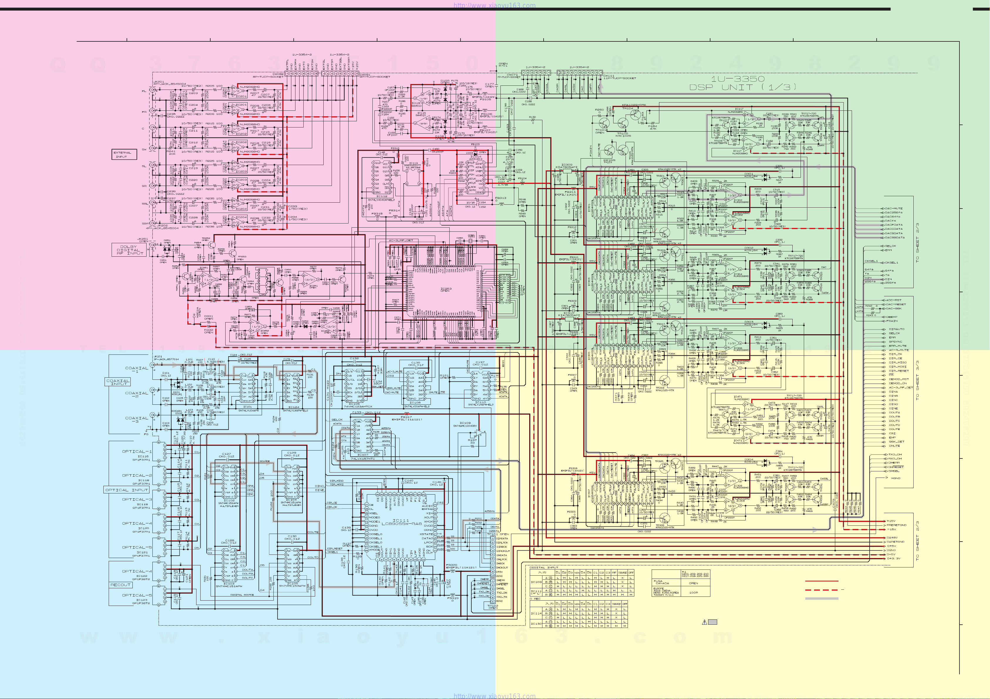
SCHEMATIC DIAGRAMS (1/9)
1 2 3 4 5 6 7 8 9 10 11
AVR-4802/AVC-A11SR
Q
Q
3
7
6
15V
0V
0V
0V
0V
-15V
3
1
5
1
2.55V
2.55V
5
5V
2.55V
2.55V
0
2.8V
2.8V
8
8V
5V
5V
9
2
4
9
A B
A B
2.8V
8
0V
0V
2
9
9
A
B
TEL 13942296513 QQ 376315150 892498299
T
E
L
1
3
9
0V 2.5V
4
2
2
5V
9
6
5
1
3
3.3V
Q
Q
3
7
6
3
1
5
1
5
0
8
9
2
-15V
4
-14V
TEL 13942296513 QQ 376315150 892498299
C
0V
D
9
8
2
9
9
E
w
w
w
C D
C D
.
x
i
a
o
y
5V
u
NOTICE
ALL RESISTANCE VALUES IN OHM. k=1,000 OHM M=1,000,000 OHM
ALL CAPACITANCE VALUES I N MICRO FARAD. P=MICRO-MICRO FARAD
EACH VOLTAGE AND CURRE NT ARE MEASUERD AT NO SIGNAL INPUT
CONDITION.
CIRCUIT AND PARTS ARE SUBJECT TO CHANGE WITHOUT PRIOR
NOTICE.
1
6
3
.
WARNING:
Parts marked with this symbol have critical characteristics.
Use ONLY replacement parts recommended by the manufacture.
CAUTION:
c
Before returning the unit to the customer, make sure you make either (1) a
leakage current check or (2) a line to chassis resistance check. If the leakage
current exceeds 0.5 milliamps, or if the resistance from chassis to either side
of the power card is less than 460 kohms, the unit is defective.
WARNING:
DO NOT return the unit to the customer until the problem is located and
corrected.
o
m
+ B LINE
- B LINE
SIGNAL LINE
SCHEMATIC DIAGRAMS (1/9)
1U-3350 DSP UNIT (1/3)
F
G
H
62
Page 64

Q
Q
SCHEMATIC DIAGRAMS (1/9)
1 2 3 4 5 6 7 8 9 10 11
3
7
6
3
1
5
1
5
0
8
9
2
4
9
8
2
9
9
TEL 13942296513 QQ 376315150 892498299
0V
0V
T
E
L
1
3
9
4
2
2
9
6
5
1
3
15V
Q
TEL 13942296513 QQ 376315150 892498299
0V
2.55V
0V
-15V
Q
3
7
6
3
1
5
1
5
0
8
9
2
2.55V
4
9
5V
8
2
9
2.55V
2.55V
9
2.8V
2.8V
w
w
w
.
x
i
a
o
y
u
1
6
3
.
c
o
m
Page 65
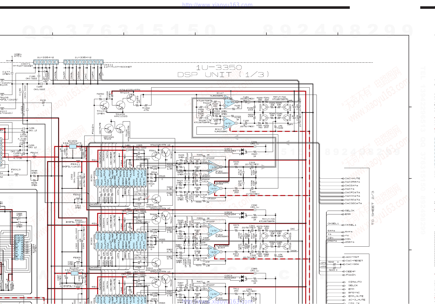
AVR-4802/AVC-A11SR
1
5V
3
7
9
5V
4
6
2
3
2
Q
TEL 13942296513 QQ 376315150 892498299
2.8V
2.8V
Q
T
E
3
8V
L
9
6
1
5
1
5
3
1
5
0
Q
Q
3
7
6
8
3
0V
1
9
5
1
2
5
0
4
8
9
9
2
8
4
9
2
8
2
9
9
9
TEL 13942296513 QQ 376315150 892498299
A
B
9
w
w
w
.
x
i
a
2.8V
o
y
u
1
6
3
0V
.
-14V
-15V
c
0V
o
C
m
D
Page 66

0V 2.5V
5V
1
3
7
9
4
6
2
3
2
Q
TEL 13942296513 QQ 376315150 892498299
Q
T
E
3
L
9
6
1
5
1
5
3
1
5
0
Q
Q
3
7
6
8
3
1
9
5
1
2
5
0
4
8
9
3.3V
9
2
8
4
9
2
8
2
9
9
9
TEL 13942296513 QQ 376315150 892498299
9
w
w
w
.
x
i
a
o
y
u
1
6
3
.
c
o
m
5V
NOTICE
ALL RESISTANCE VALUES IN OHM. k=1,000 OHM M=1,000,000 OHM
ALL CAPACITANCE VALUES I N MICRO FARAD. P=MICRO-MICRO FARAD
EACH VOLTAGE AND CURRE NT ARE MEASUERD AT NO SIGNAL INPUT
CONDITION.
CIRCUIT AND PARTS ARE SUBJECT TO CHANGE WITHOUT PRIOR
NOTICE.
Page 67

1
3
7
9
4
6
2
3
2
Q
TEL 13942296513 QQ 376315150 892498299
Q
T
E
3
L
9
6
1
5
1
5
3
1
5
0
Q
Q
3
7
6
8
3
1
9
5
1
2
5
0
4
8
9
9
2
8
4
9
2
8
2
9
9
9
9
E
TEL 13942296513 QQ 376315150 892498299
F
w
w
w
.
x
WARNING:
Parts marked with this symbol have critical characteristics.
Use ONLY replacement parts recommended by the manufacture.
CAUTION:
Before returning the unit to the customer, make sure you make either (1) a
leakage current check or (2) a line to chassis resistance check. If the leakage
current exceeds 0.5 milliamps, or if the resistance from chassis to either side
of the power card is less than 460 kohms, the unit is defective.
WARNING:
i
a
DO NOT return the unit to the customer until the problem is located and
corrected.
o
y
u
1
6
3
.
+ B LINE
- B LINE
SIGNAL LINE
SCHEMATIC DIAGRAMS (1/9)
1U-3350 DSP UNIT (1/3)
c
o
m
G
H
62
Page 68

SCHEMATIC DIAGRAMS (2/9)
1 2 3 4 5 6 7 8 9 10 11
AVR-4802/AVC-A11SR
Q
Q
3
7
6
3
1
5
1
5
0
8
9
2
4
9
8
2
9
9
A
B
TEL 13942296513 QQ 376315150 892498299
T
E
L
1
3
9
4
2
2
9
6
5
1
3
3.3V
Q
Q
3
7
6
3
1
5
1
5
3.3V
0
8
9
2
4
9
8
2
9
9
TEL 13942296513 QQ 376315150 892498299
C
D
E
w
w
w
.
3.3V
x
i
a
o
y
u
NOTICE
ALL RESISTANCE VALUES IN OHM. k=1,000 OHM M=1,000,000 OHM
ALL CAPACITANCE VALUES I N MICRO FARAD. P=MICRO-MICRO FARAD
EACH VOLTAGE AND CURRE NT ARE MEASUERD AT NO SIGNAL INPUT
CONDITION.
CIRCUIT AND PARTS ARE SUBJECT TO CHANGE WITHOUT PRIOR
NOTICE.
1
6
3
.
WARNING:
Parts marked with this symbol have critical characteristics.
Use ONLY replacement parts recommended by the manufacture.
CAUTION:
Before returning the unit to the customer, make sure you make either (1) a
c
leakage current check or (2) a line to chassis resistance check. If the leakage
current exceeds 0.5 milliamps, or if the resistance from chassis to either side
of the power card is less than 460 kohms, the unit is defective.
WARNING:
DO NOT return the unit to the customer until the problem is located and
corrected.
o
m
F
G
+ B LINE
- B LINE
SIGNAL LINE
H
SCHEMATIC DIAGRAMS (2/9)
1U-3350 DSP UNIT (2/3)
63
Page 69

SCHEMATIC DIAGRAMS (2/9)
1 2 3 4 5 6 7 8 9 10 11
AVR-4802/AVC-A11SR
Q
Q
3
7
6
3
A
A
1
5
1
5
0
8
9
2
4
B
B
9
8
2
9
9
A
B
TEL 13942296513 QQ 376315150 892498299
T
E
L
1
3
9
4
2
2
9
6
5
1
3
3.3V
Q
Q
3
7
6
3
1
5
1
5
3.3V
0
8
9
2
4
9
8
2
9
9
TEL 13942296513 QQ 376315150 892498299
C
D
E
w
w
w
3.3V
C
C
.
x
i
a
o
y
u
NOTICE
ALL RESISTANCE VALUES IN OHM. k=1,000 OHM M=1,000,000 OHM
ALL CAPACITANCE VALUES I N MICRO FARAD. P=MICRO-MICRO FARAD
EACH VOLTAGE AND CURRE NT ARE MEASUERD AT NO SIGNAL INPUT
CONDITION.
CIRCUIT AND PARTS ARE SUBJECT TO CHANGE WITHOUT PRIOR
NOTICE.
1
6
3
.
D
D
WARNING:
Parts marked with this symbol have critical characteristics.
Use ONLY replacement parts recommended by the manufacture.
CAUTION:
Before returning the unit to the customer, make sure you make either (1) a
c
leakage current check or (2) a line to chassis resistance check. If the leakage
current exceeds 0.5 milliamps, or if the resistance from chassis to either side
of the power card is less than 460 kohms, the unit is defective.
WARNING:
DO NOT return the unit to the customer until the problem is located and
corrected.
o
m
F
G
+ B LINE
- B LINE
SIGNAL LINE
H
SCHEMATIC DIAGRAMS (2/9)
1U-3350 DSP UNIT (2/3)
63
Page 70

Q
Q
SCHEMATIC DIAGRAMS (2/9)
1 2 3 4 5 6 7 8 9 10 11
3
7
6
3
1
5
1
5
0
8
9
2
4
9
8
2
9
9
TEL 13942296513 QQ 376315150 892498299
T
E
L
1
3
9
4
2
2
9
6
5
1
3
Q
Q
3
7
6
3
1
5
1
5
0
8
9
2
4
9
8
2
9
TEL 13942296513 QQ 376315150 892498299
9
w
w
w
.
x
i
a
o
y
u
1
6
3
.
c
o
m
Page 71

AVR-4802/AVC-A11SR
1
3
7
9
4
6
2
3
2
Q
TEL 13942296513 QQ 376315150 892498299
Q
T
E
3
L
9
6
1
5
1
5
3
1
5
0
Q
Q
3
7
6
8
3
1
9
5
1
2
5
0
4
8
9
9
2
8
4
9
2
8
2
9
9
9
TEL 13942296513 QQ 376315150 892498299
A
B
9
w
w
w
.
x
i
a
o
y
u
1
6
3
.
c
o
C
m
D
Page 72
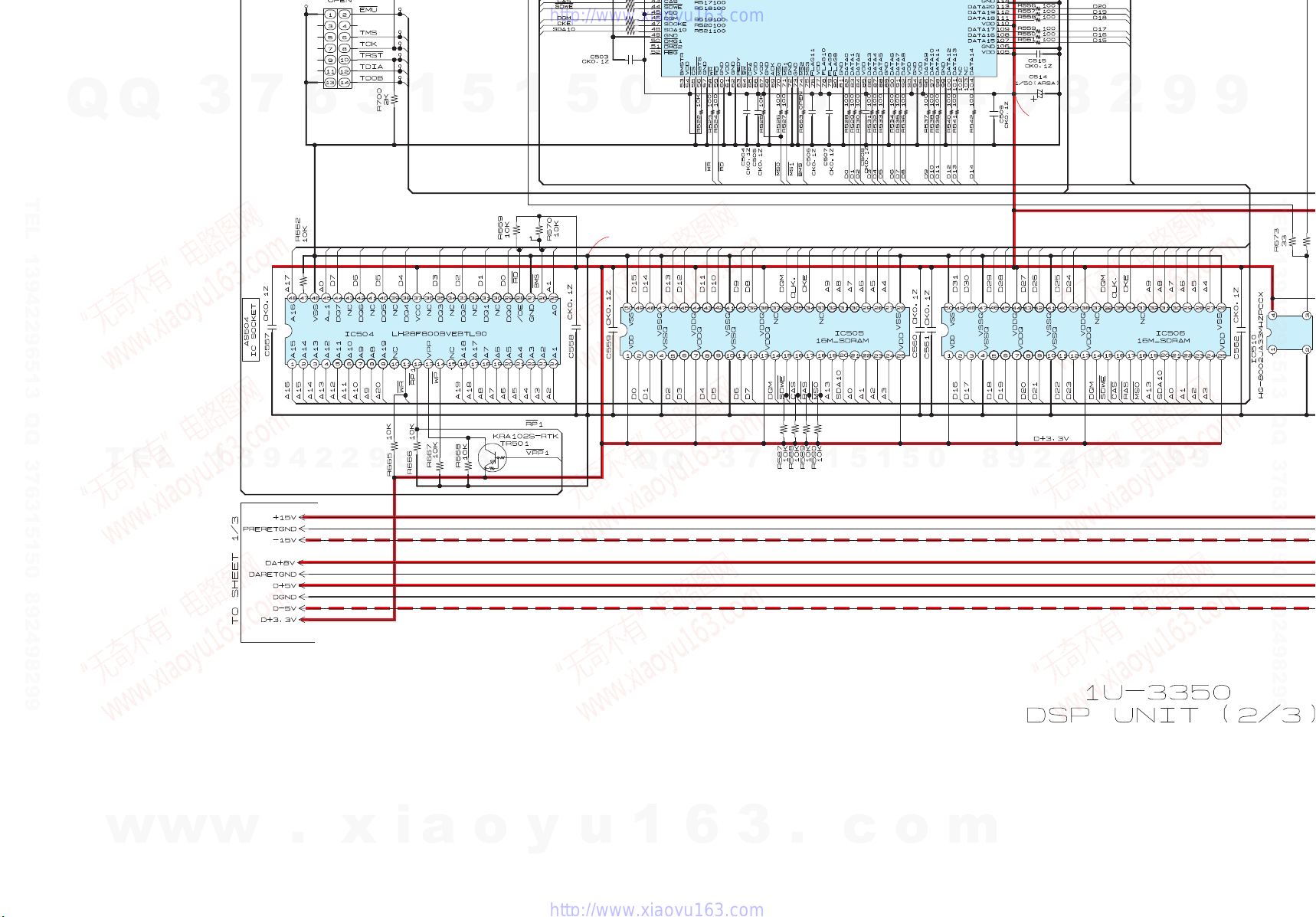
1
3
7
9
4
6
2
3
2
Q
TEL 13942296513 QQ 376315150 892498299
Q
T
E
3
L
9
6
1
5
1
5
3
1
5
0
3.3V
Q
Q
3
7
6
8
3
1
9
5
1
2
5
0
4
8
9
9
3.3V
2
8
4
9
2
8
2
9
9
9
TEL 13942296513 QQ 376315150 892498299
9
w
w
w
.
x
i
a
o
y
u
1
6
3
.
c
o
m
NOTICE
ALL RESISTANCE VALUES IN OHM. k=1,000 OHM M=1,000,000 OHM
ALL CAPACITANCE VALUES I N MICRO FARAD. P=MICRO-MICRO FARAD
EACH VOLTAGE AND CURRE NT ARE MEASUERD AT NO SIGNAL INPUT
CONDITION.
CIRCUIT AND PARTS ARE SUBJECT TO CHANGE WITHOUT PRIOR
NOTICE.
Page 73

1
3
7
9
4
6
2
3
2
Q
TEL 13942296513 QQ 376315150 892498299
Q
T
E
3
L
9
6
1
5
1
5
3
1
5
3.3V
0
Q
Q
3
7
6
8
3
1
9
5
1
2
5
0
4
8
9
9
2
8
4
9
2
8
2
9
9
9
9
E
TEL 13942296513 QQ 376315150 892498299
F
w
w
w
.
x
WARNING:
Parts marked with this symbol have critical characteristics.
Use ONLY replacement parts recommended by the manufacture.
CAUTION:
Before returning the unit to the customer, make sure you make either (1) a
leakage current check or (2) a line to chassis resistance check. If the leakage
current exceeds 0.5 milliamps, or if the resistance from chassis to either side
of the power card is less than 460 kohms, the unit is defective.
WARNING:
i
a
DO NOT return the unit to the customer until the problem is located and
corrected.
o
y
u
1
6
3
.
+ B LINE
- B LINE
SIGNAL LINE
SCHEMATIC DIAGRAMS (2/9)
1U-3350 DSP UNIT (2/3)
c
o
m
G
H
63
Page 74

SCHEMATIC DIAGRAMS (3/9)
1 2 3 4 5 6 7 8 9 10 11
AVR-4802/AVC-A11SR
Q
Q
3
7
6
3
1
5
1
5
0
5.1V
8
0V
0V
0V
9
2
0V
4
0V
9
8
2
9
9
A
B
TEL 13942296513 QQ 376315150 892498299
T
E
L
1
3
9
4
2
2
9
6
5
1
3
4.8V
Q
Q
3
7
6
3
1
5
1
5
4.9V
0
8
9
2
4
9
8
2
9
9
TEL 13942296513 QQ 376315150 892498299
C
D
E
w
w
w
.
x
i
a
o
y
u
NOTICE
ALL RESISTANCE VALUES IN OHM. k=1,000 OHM M=1,000,000 OHM
ALL CAPACITANCE VALUES I N MICRO FARAD. P=MICRO-MICRO FARAD
EACH VOLTAGE AND CURRE NT ARE MEASUERD AT NO SIGNAL INPUT
CONDITION.
CIRCUIT AND PARTS ARE SUBJECT TO CHANGE WITHOUT PRIOR
NOTICE.
1
6
3
.
5.1V
4.9V
5.6V
WARNING:
Parts marked with this symbol have critical characteristics.
Use ONLY replacement parts recommended by the manufacture.
CAUTION:
Before returning the unit to the customer, make sure you make either (1) a
c
leakage current check or (2) a line to chassis resistance check. If the leakage
current exceeds 0.5 milliamps, or if the resistance from chassis to either side
of the power card is less than 460 kohms, the unit is defective.
WARNING:
DO NOT return the unit to the customer until the problem is located and
corrected.
o
m
5.1V
F
G
+ B LINE
- B LINE
SIGNAL LINE
H
SCHEMATIC DIAGRAMS (3/9)
1U-3350 DSP UNIT (3/3)
64
Page 75

SCHEMATIC DIAGRAMS (3/9)
1 2 3 4 5 6 7 8 9 10 11
AVR-4802/AVC-A11SR
Q
Q
3
7
6
3
A
A
1
5
1
5
0
5.1V
8
0V
0V
0V
9
2
0V
4
0V
9
8
2
9
9
A
B
B
B
TEL 13942296513 QQ 376315150 892498299
T
E
L
1
3
9
4
2
2
9
6
5
1
3
4.8V
Q
Q
3
7
6
3
1
5
1
5
4.9V
0
8
9
2
4
9
8
2
9
9
TEL 13942296513 QQ 376315150 892498299
C
D
E
w
w
w
C
C
.
x
i
a
o
y
u
NOTICE
ALL RESISTANCE VALUES IN OHM. k=1,000 OHM M=1,000,000 OHM
ALL CAPACITANCE VALUES I N MICRO FARAD. P=MICRO-MICRO FARAD
EACH VOLTAGE AND CURRE NT ARE MEASUERD AT NO SIGNAL INPUT
CONDITION.
CIRCUIT AND PARTS ARE SUBJECT TO CHANGE WITHOUT PRIOR
NOTICE.
1
6
3
.
5.1V
4.9V
5.6V
5.1V
D
D
WARNING:
Parts marked with this symbol have critical characteristics.
Use ONLY replacement parts recommended by the manufacture.
CAUTION:
c
Before returning the unit to the customer, make sure you make either (1) a
leakage current check or (2) a line to chassis resistance check. If the leakage
current exceeds 0.5 milliamps, or if the resistance from chassis to either side
of the power card is less than 460 kohms, the unit is defective.
WARNING:
DO NOT return the unit to the customer until the problem is located and
corrected.
o
m
F
G
+ B LINE
- B LINE
SIGNAL LINE
H
SCHEMATIC DIAGRAMS (3/9)
1U-3350 DSP UNIT (3/3)
64
Page 76
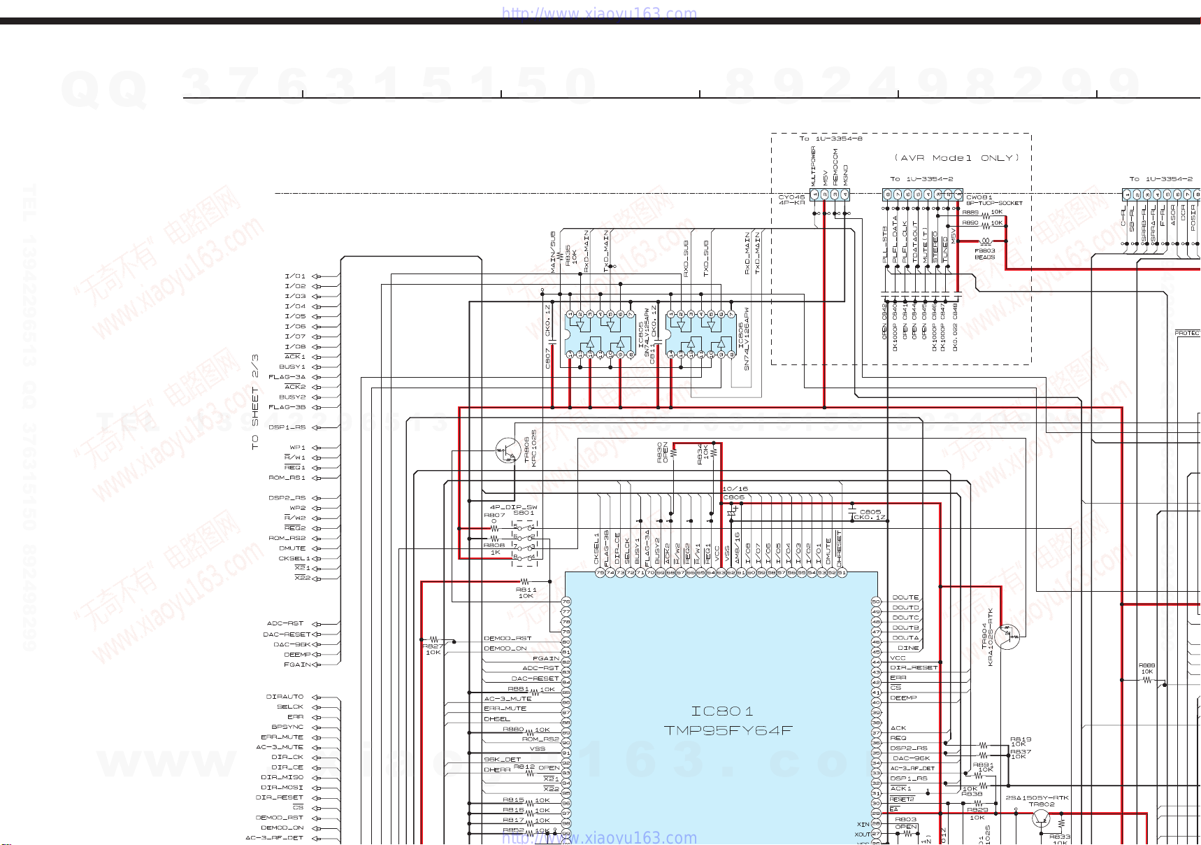
Q
Q
SCHEMATIC DIAGRAMS (3/9)
1 2 3 4 5 6 7 8 9 10 11
3
7
6
3
1
5
1
5
0
8
9
2
4
9
8
2
9
9
TEL 13942296513 QQ 376315150 892498299
T
E
L
1
3
9
4
2
2
9
6
5
1
3
Q
Q
3
7
6
3
1
5
1
5
0
8
9
2
4
9
8
2
9
TEL 13942296513 QQ 376315150 892498299
9
w
w
w
.
x
i
a
o
y
u
1
6
3
.
c
o
m
4.8V
Page 77

AVR-4802/AVC-A11SR
1
0V
3
7
9
4
6
0V
2
3
2
Q
TEL 13942296513 QQ 376315150 892498299
Q
5.1V
T
E
3
L
9
1
0V
6
5
1
5
3
1
0V
5
0
0V
Q
Q
3
7
6
8
3
1
9
5
1
2
5
0
4
8
9
9
2
8
4
9
2
8
2
9
9
9
TEL 13942296513 QQ 376315150 892498299
A
B
9
w
w
w
.
x
i
a
o
y
u
1
6
3
.
c
o
C
m
D
Page 78

1
3
7
9
4
6
2
3
2
Q
TEL 13942296513 QQ 376315150 892498299
Q
T
E
3
L
9
6
1
5
1
5
3
1
5
0
Q
Q
3
7
6
8
3
1
9
5
1
2
5
0
4
8
9
9
2
8
4
9
2
8
2
9
9
9
TEL 13942296513 QQ 376315150 892498299
9
w
w
w
.
x
i
a
o
y
u
1
6
3
.
c
o
m
NOTICE
ALL RESISTANCE VALUES IN OHM. k=1,000 OHM M=1,000,000 OHM
ALL CAPACITANCE VALUES I N MICRO FARAD. P=MICRO-MICRO FARAD
EACH VOLTAGE AND CURRE NT ARE MEASUERD AT NO SIGNAL INPUT
CONDITION.
CIRCUIT AND PARTS ARE SUBJECT TO CHANGE WITHOUT PRIOR
NOTICE.
Page 79

1
3
7
9
4
6
2
3
2
Q
TEL 13942296513 QQ 376315150 892498299
Q
T
E
3
L
9
6
1
5
1
5
4.9V
3
1
4.9V
5
5.6V
0
5.1V
Q
Q
5.1V
3
7
6
8
3
1
9
5
1
2
5
0
4
8
9
9
2
8
4
9
2
8
2
9
9
9
9
E
TEL 13942296513 QQ 376315150 892498299
F
w
w
w
.
x
WARNING:
Parts marked with this symbol have critical characteristics.
Use ONLY replacement parts recommended by the manufacture.
CAUTION:
Before returning the unit to the customer, make sure you make either (1) a
leakage current check or (2) a line to chassis resistance check. If the leakage
current exceeds 0.5 milliamps, or if the resistance from chassis to either side
of the power card is less than 460 kohms, the unit is defective.
WARNING:
i
a
DO NOT return the unit to the customer until the problem is located and
corrected.
o
y
u
1
6
3
.
+ B LINE
- B LINE
SIGNAL LINE
SCHEMATIC DIAGRAMS (3/9)
1U-3350 DSP UNIT (3/3)
c
o
m
G
H
64
Page 80

SCHEMATIC DIAGRAMS (4/9)
1 2 3 4 5 6 7 8 9 10 11
AVR-4802/AVC-A11SR
Q
Q
3
7
0V
0V
0V
0V
6
3
0V
0V
0V
0V
1
5
1
5
0
8
0V
0V
0V
9
2
4
20V
0.1V
4.5V
9
8
0V
0V
2
20V
20V
0V
9
9
A
B
TEL 13942296513 QQ 376315150 892498299
T
E
L
1
3
9
4
2
2
9
6
5
1
- 15.2
+ 15.1
3
Q
Q
3
7
6
3
1
5
1
5
0
5.1V
5.1V
5.1V
5.1V
20V
0.1V
4.5V
8
9
2
4
9
59.8V
8
2
9
9
TEL 13942296513 QQ 376315150 892498299
C
D
E
5.1V
4.5V
5.1V
59.8V
5V
- 14.5V ´ 7
4.8V
F
8.0V
0V
G
- 14.5V
5V
5V
5V
5V
5V
5V
5V
w
w
w
.
x
i
a
o
y
u
NOTICE
ALL RESISTANCE VALUES IN OHM. k=1,000 OHM M=1,000,000 OHM
ALL CAPACITANCE VALUES I N MICRO FARAD. P=MICRO-MICRO FARAD
EACH VOLTAGE AND CURRE NT ARE MEASUERD AT NO SIGNAL INPUT
CONDITION.
CIRCUIT AND PARTS ARE SUBJECT TO CHANGE WITHOUT PRIOR
NOTICE.
1
6
3
.
WARNING:
Parts marked with this symbol have critical characteristics.
Use ONLY replacement parts recommended by the manufacture.
CAUTION:
Before returning the unit to the customer, make sure you make either (1) a
c
leakage current check or (2) a line to chassis resistance check. If the leakage
current exceeds 0.5 milliamps, or if the resistance from chassis to either side
of the power card is less than 460 kohms, the unit is defective.
WARNING:
DO NOT return the unit to the customer until the problem is located and
corrected.
o
m
+ B LINE
- B LINE
SIGNAL LINE
H
SCHEMATIC DIAGRAMS (4/9)
1U-3351 AUDIO IN UNIT
65
Page 81

SCHEMATIC DIAGRAMS (4/9)
1 2 3 4 5 6 7 8 9 10 11
AVR-4802/AVC-A11SR
Q
Q
3
7
0V
0V
0V
0V
6
0V
0V
A
A
3
0V
0V
1
5
1
5
0
2
20V
20V
0V
9
9
A
B
20V
4
0.1V
4.5V
9
8
0V
0V
8
0V
0V
0V
9
2
B
B
TEL 13942296513 QQ 376315150 892498299
T
E
L
1
3
9
4
2
2
9
6
5
1
- 15.2
+ 15.1
3
Q
Q
3
7
6
3
1
5
1
5
0
5.1V
5.1V
5.1V
5.1V
20V
0.1V
4.5V
8
9
2
4
9
59.8V
8
2
9
9
TEL 13942296513 QQ 376315150 892498299
C
D
E
C
C
5.1V
4.5V
B LINE
5.1V
59.8V
5V
- 14.5V ´ 7
4.8V
F
8.0V
0V
- 14.5V
5V
5V
5V
5V
5V
5V
5V
D
D
G
w
w
w
.
x
i
a
o
y
u
NOTICE
ALL RESISTANCE VALUES IN OHM. k=1,000 OHM M=1,000,000 OHM
ALL CAPACITANCE VALUES I N MICRO FARAD. P=MICRO-MICRO FARAD
EACH VOLTAGE AND CURRE NT ARE MEASUERD AT NO SIGNAL INPUT
CONDITION.
CIRCUIT AND PARTS ARE SUBJECT TO CHANGE WITHOUT PRIOR
NOTICE.
1
6
3
.
WARNING:
Parts marked with this symbol have critical characteristics.
Use ONLY replacement parts recommended by the manufacture.
CAUTION:
c
Before returning the unit to the customer, make sure you make either (1) a
leakage current check or (2) a line to chassis resistance check. If the leakage
current exceeds 0.5 milliamps, or if the resistance from chassis to either side
of the power card is less than 460 kohms, the unit is defective.
WARNING:
DO NOT return the unit to the customer until the problem is located and
corrected.
o
m
+ B LINE
- B LINE
SIGNAL LINE
H
SCHEMATIC DIAGRAMS (4/9)
1U-3351 AUDIO IN UNIT
65
Page 82

Q
Q
SCHEMATIC DIAGRAMS (4/9)
1 2 3 4 5 6 7 8 9 10 11
3
7
6
3
1
5
1
5
0
8
9
2
4
9
8
2
9
9
TEL 13942296513 QQ 376315150 892498299
T
E
L
1
3
9
4
2
2
9
6
5
1
0V
0V
3
0V
TEL 13942296513 QQ 376315150 892498299
0V
0V
0V
Q
Q
0V
0V
9
9
2
8
9
4
2
9
3
7
6
3
1
5
1
5
0
8
w
w
w
.
x
i
a
o
y
u
1
6
3
.
c
o
m
- 15.2
+ 15.1
Page 83

AVR-4802/AVC-A11SR
1
3
7
9
4
6
2
3
2
Q
TEL 13942296513 QQ 376315150 892498299
Q
T
0V
E
3
L
0V
0V
9
6
1
5
1
5
3
1
5
0
20V
Q
0.1V
4.5V
Q
3
7
6
8
3
1
9
5
1
2
0V
0V
5
0
4
8
20V
20V
9
9
0V
2
8
4
9
2
8
2
9
9
9
TEL 13942296513 QQ 376315150 892498299
A
B
9
w
w
w
.
x
i
a
o
20V
0.1V
4.5V
5.1V
y
u
5.1V
1
6
3
.
c
o
C
m
D
Page 84

1
3
7
9
4
6
2
3
2
Q
TEL 13942296513 QQ 376315150 892498299
Q
T
E
3
L
9
6
1
5
1
5
3
1
5
0
Q
Q
3
7
6
8
3
1
9
5
1
2
5
0
4
8
9
9
2
8
4
9
2
8
2
9
9
9
TEL 13942296513 QQ 376315150 892498299
9
w
w
w
.
x
i
a
o
y
u
1
6
3
.
c
o
m
NOTICE
ALL RESISTANCE VALUES IN OHM. k=1,000 OHM M=1,000,000 OHM
ALL CAPACITANCE VALUES I N MICRO FARAD. P=MICRO-MICRO FARAD
EACH VOLTAGE AND CURRE NT ARE MEASUERD AT NO SIGNAL INPUT
CONDITION.
CIRCUIT AND PARTS ARE SUBJECT TO CHANGE WITHOUT PRIOR
NOTICE.
Page 85

5.1V
1
5.1V
3
7
9
4
6
4.5V
2
3
2
Q
TEL 13942296513 QQ 376315150 892498299
Q
T
E
3
L
5V
9
- 14.5V
6
1
5
5
5V
1
1
5V
3
5
5V
0
5.1V
5.1V
5V
5V
Q
Q
3
5V
7
5V
- 14.5V ´ 7
6
8
3
4.8V
1
9
5
1
0V
2
59.8V
5
59.8V
0
4
8.0V
8
9
9
2
8
4
9
2
8
2
9
9
9
9
E
TEL 13942296513 QQ 376315150 892498299
F
w
w
w
.
x
WARNING:
Parts marked with this symbol have critical characteristics.
Use ONLY replacement parts recommended by the manufacture.
CAUTION:
Before returning the unit to the customer, make sure you make either (1) a
leakage current check or (2) a line to chassis resistance check. If the leakage
current exceeds 0.5 milliamps, or if the resistance from chassis to either side
of the power card is less than 460 kohms, the unit is defective.
WARNING:
i
a
DO NOT return the unit to the customer until the problem is located and
corrected.
o
y
u
1
6
3
.
+ B LINE
- B LINE
SIGNAL LINE
SCHEMATIC DIAGRAMS (4/9)
1U-3351 AUDIO IN UNIT
c
o
m
G
H
65
Page 86

SCHEMATIC DIAGRAMS (5/9)
1 2 3 4 5 6 7 8 9 10 11
AVR-4802/AVC-A11SR
Q
Q
3
7
6
3
1
5
1
5
0
8
0V
0.1V
0V
0.1V
9
2
4
9
8
2
9
9
A
B
TEL 13942296513 QQ 376315150 892498299
T
E
L
1
3
9
4
2
2
9
6
5
1
3
5.1V
5.1V
Q
5.1V
Q
3
7
6
3
1
5
1
5
0
8
9
2
4
9
8
2
9
9
TEL 13942296513 QQ 376315150 892498299
C
D
E
- 5
+ 5
0.1V
0.1V
NOTICE
ALL RESISTANCE VALUES IN OHM. k=1,000 OHM M=1,000,000 OHM
ALL CAPACITANCE VALUES I N MICRO FARAD. P=MICRO-MICRO FARAD
EACH VOLTAGE AND CURRE NT ARE MEASUERD AT NO SIGNAL INPUT
CONDITION.
CIRCUIT AND PARTS ARE SUBJECT TO CHANGE WITHOUT PRIOR
NOTICE.
F
WARNING:
Parts marked with this symbol have critical characteristics.
Use ONLY replacement parts recommended by the manufacture.
CAUTION:
Before returning the unit to the customer, make sure you make either (1) a
leakage current check or (2) a line to chassis resistance check. If the leakage
current exceeds 0.5 milliamps, or if the resistance from chassis to either side
of the power card is less than 460 kohms, the unit is defective.
WARNING:
DO NOT return the unit to the customer until the problem is located and
corrected.
G
+ B LINE
- B LINE
SIGNAL LINE
w
w
w
.
x
i
a
o
y
u
1
6
3
.
c
o
m
H
SCHEMATIC DIAGRAMS (5/9)
1U-3351-2 S-VIDEO UNIT
66
Page 87
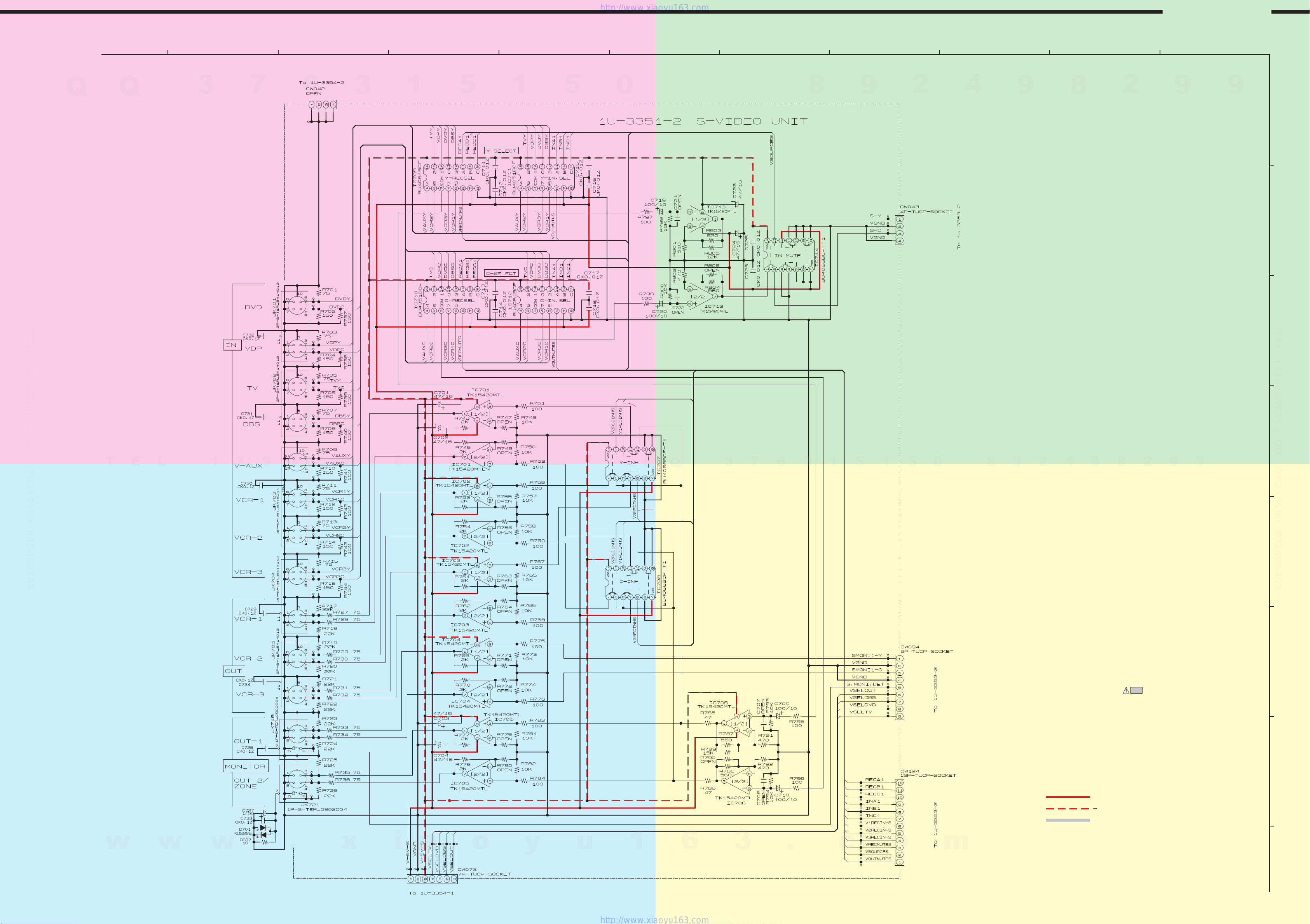
SCHEMATIC DIAGRAMS (5/9)
1 2 3 4 5 6 7 8 9 10 11
AVR-4802/AVC-A11SR
Q
Q
3
7
6
3
A
A
1
5
1
5
0
8
0V
0.1V
9
2
4
9
8
2
9
9
A
B
B
B
0V
0.1V
TEL 13942296513 QQ 376315150 892498299
T
E
L
1
3
9
4
2
2
9
6
5
1
3
5.1V
5.1V
Q
5.1V
Q
3
7
6
3
1
5
1
5
0
8
9
2
4
9
8
2
9
9
TEL 13942296513 QQ 376315150 892498299
C
D
E
C
C
- 5
+ 5
0.1V
0.1V
NOTICE
ALL RESISTANCE VALUES IN OHM. k=1,000 OHM M=1,000,000 OHM
ALL CAPACITANCE VALUES I N MICRO FARAD. P=MICRO-MICRO FARAD
EACH VOLTAGE AND CURRE NT ARE MEASUERD AT NO SIGNAL INPUT
CONDITION.
CIRCUIT AND PARTS ARE SUBJECT TO CHANGE WITHOUT PRIOR
NOTICE.
WARNING:
Parts marked with this symbol have critical characteristics.
Use ONLY replacement parts recommended by the manufacture.
CAUTION:
Before returning the unit to the customer, make sure you make either (1) a
leakage current check or (2) a line to chassis resistance check. If the leakage
current exceeds 0.5 milliamps, or if the resistance from chassis to either side
D
D
of the power card is less than 460 kohms, the unit is defective.
WARNING:
DO NOT return the unit to the customer until the problem is located and
corrected.
F
G
+ B LINE
- B LINE
SIGNAL LINE
w
w
w
.
x
i
a
o
y
u
1
6
3
.
c
o
m
H
SCHEMATIC DIAGRAMS (5/9)
1U-3351-2 S-VIDEO UNIT
66
Page 88
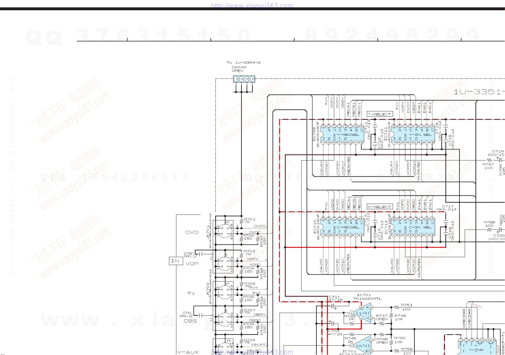
Q
Q
SCHEMATIC DIAGRAMS (5/9)
1 2 3 4 5 6 7 8 9 10 11
3
7
6
3
1
5
1
5
0
8
9
2
4
9
8
2
9
9
TEL 13942296513 QQ 376315150 892498299
T
E
L
1
3
9
4
2
2
9
6
5
1
3
Q
Q
3
7
6
3
1
5
1
5
0
8
9
2
4
9
8
2
9
TEL 13942296513 QQ 376315150 892498299
9
w
w
w
.
x
i
a
o
y
u
1
6
3
.
c
o
m
5.1V
5.1V
Page 89

AVR-4802/AVC-A11SR
1
3
7
9
4
6
0.1V
2
3
2
Q
TEL 13942296513 QQ 376315150 892498299
0V
Q
T
E
3
L
9
6
1
5
1
5
3
1
5
0
Q
Q
3
7
6
8
3
1
9
5
1
2
5
0
4
8
9
9
2
8
4
9
2
8
2
9
9
9
TEL 13942296513 QQ 376315150 892498299
A
B
9
0V
w
w
0.1V
w
.
x
i
a
o
y
u
1
6
3
.
c
o
C
m
D
Page 90

1
3
7
9
4
6
2
3
2
Q
TEL 13942296513 QQ 376315150 892498299
Q
T
E
3
L
9
6
1
5
1
5
3
1
5
0
Q
Q
3
7
6
8
3
1
9
5
1
2
5
0
4
8
9
9
2
8
4
9
2
8
2
9
9
9
5.1V
TEL 13942296513 QQ 376315150 892498299
9
w
w
w
.
x
i
a
o
y
u
1
6
3
- 5
.
c
+ 5
o
m
Page 91

5.1V
Q
TEL 13942296513 QQ 376315150 892498299
Q
T
0.1V
0.1V
E
3
L
1
3
7
9
4
6
2
2
3
9
6
1
5
1
5
3
1
5
0
Q
Q
3
1
9
5
8
NOTICE
ALL RESISTANCE VALUES IN OHM. k=1,000 OHM M=1,000,000 OHM
ALL CAPACITANCE VALUES I N MICRO FARAD. P=MICRO-MICRO FARAD
EACH VOLTAGE AND CURRE NT ARE MEASUERD AT NO SIGNAL INPUT
CONDITION.
CIRCUIT AND PARTS ARE SUBJECT TO CHANGE WITHOUT PRIOR
NOTICE.
WARNING:
Parts marked with this symbol have critical characteristics.
3
6
7
Use ONLY replacement parts recommended by the manufacture.
CAUTION:
Before returning the unit to the customer, make sure you make either (1) a
leakage current check or (2) a line to chassis resistance check. If the leakage
current exceeds 0.5 milliamps, or if the resistance from chassis to either side
of the power card is less than 460 kohms, the unit is defective.
WARNING:
DO NOT return the unit to the customer until the problem is located and
corrected.
1
2
5
0
4
8
9
9
2
8
4
9
2
8
2
9
9
9
9
E
TEL 13942296513 QQ 376315150 892498299
F
G
w
w
w
.
x
i
a
o
y
u
1
6
3
+ B LINE
- B LINE
SIGNAL LINE
SCHEMATIC DIAGRAMS (5/9)
1U-3351-2 S-VIDEO UNIT
.
c
o
m
H
66
Page 92

SCHEMATIC DIAGRAMS (6/9)
1 2 3 4 5 6 7 8 9 10 11
AVR-4802/AVC-A11SR
Q
TEL 13942296513 QQ 376315150 892498299
Q
3
7
6
3
1
5
1
- 5V
5V
5
0
59.5V
- 59.5V
8
9
12V
5V
5V
AVR Model only
2
20V
- 15.0V
+ 14.4V
15.0V
4
20V
9
20V
24.2V
- 24.2V
8
13.1V
2
9
9
A
B
TEL 13942296513 QQ 376315150 892498299
C
T
E
L
1
3
9
4
2
2
9
6
5
1
3
0V
4.8V
- 5V
- 5V
Q
5V
Q
3
7
6
3
1
5
1
5
0
- 14.4V
5.1V
8
9
2
4
- 13.1V
9
5.1V
8
5.1V
2
9
D
9
E
5.1V
2.6V
4.4V
1.8V
4.9V
3.25V
3.1V
4V
0V
1.44V
2.9V
- 5V
2.86V
2.37V
5V
5V 5V 5V 5V 5V
+ B LINE
- B LINE
SIGNAL LINE
F
G
w
w
w
.
x
i
a
o
y
u
NOTICE
ALL RESISTANCE VALUES IN OHM. k=1,000 OHM M=1,000,000 OHM
ALL CAPACITANCE VALUES I N MICRO FARAD. P=MICRO-MICRO FARAD
EACH VOLTAGE AND CURRE NT ARE MEASUERD AT NO SIGNAL INPUT
CONDITION.
CIRCUIT AND PARTS ARE SUBJECT TO CHANGE WITHOUT PRIOR
NOTICE.
1
6
3
.
WARNING:
Parts marked with this symbol have critical characteristics.
Use ONLY replacement parts recommended by the manufacture.
CAUTION:
Before returning the unit to the customer, make sure you make either (1) a
c
leakage current check or (2) a line to chassis resistance check. If the leakage
current exceeds 0.5 milliamps, or if the resistance from chassis to either side
of the power card is less than 460 kohms, the unit is defective.
WARNING:
DO NOT return the unit to the customer until the problem is located and
corrected.
o
m
SCHEMATIC DIAGRAMS (6/9)
1U-3353-1 C VIDEO & REG. UNIT
1U-3353-2 OSD UNIT
1U-3353-3 MASTER VR UNIT
1U-3353-4 AC OUTLET UNIT
1U-3353-5P.SW UNLOCK UNIT
1U-3353-6 P.SW LOCK UNIT (AVC MODEL ONLY)
H
67
Page 93
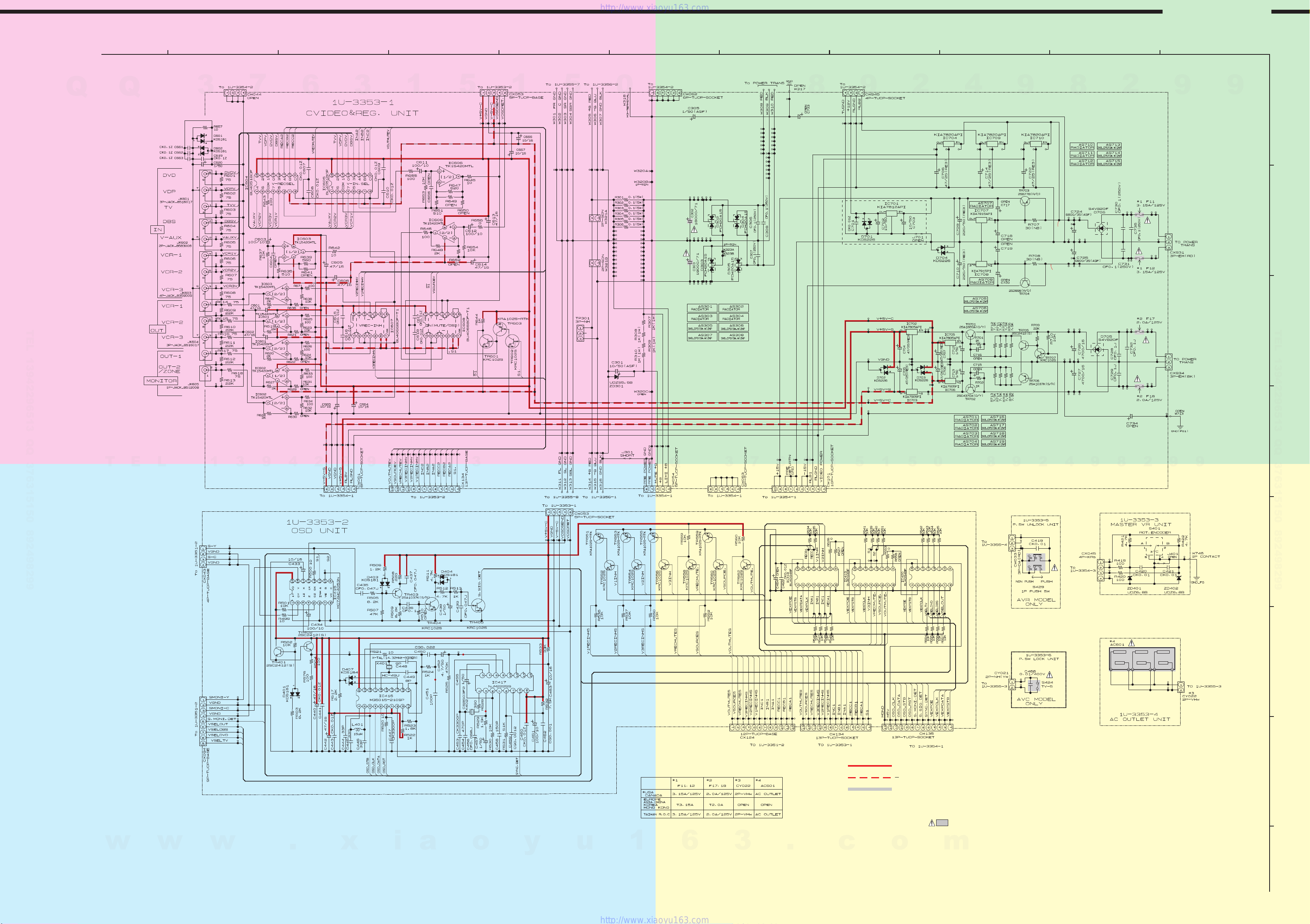
SCHEMATIC DIAGRAMS (6/9)
1 2 3 4 5 6 7 8 9 10 11
AVR-4802/AVC-A11SR
Q
Q
3
7
6
3
A
A
1
5
1
- 5V
5V
5
0
59.5V
- 59.5V
8
9
12V
AVR Model only
2
20V
4
20V
15.0V
B
B
- 15.0V
9
20V
24.2V
- 24.2V
8
2
9
9
A
B
TEL 13942296513 QQ 376315150 892498299
T
E
L
1
3
9
4
2
2
9
6
5
1
3
4.8V
Q
Q
3
7
6
3
1
5V
5V
5
- 5V
- 5V
1
5
0
+ 14.4V
- 14.4V
8
9
2
13.1V
0V
- 13.1V
4
9
8
2
9
9
TEL 13942296513 QQ 376315150 892498299
C
D
2.6V
C
C
4.4V
1.8V
4.9V
3.25V
5V
5.1V
3.1V
4V
0V
1.44V
2.9V
- 5V
2.86V
2.37V
5V
5V 5V 5V 5V 5V
5.1V
5.1V
5.1V
E
F
D
D
+ B LINE
- B LINE
SIGNAL LINE
G
w
w
w
.
x
i
a
o
y
u
NOTICE
ALL RESISTANCE VALUES IN OHM. k=1,000 OHM M=1,000,000 OHM
ALL CAPACITANCE VALUES I N MICRO FARAD. P=MICRO-MICRO FARAD
EACH VOLTAGE AND CURRE NT ARE MEASUERD AT NO SIGNAL INPUT
CONDITION.
CIRCUIT AND PARTS ARE SUBJECT TO CHANGE WITHOUT PRIOR
NOTICE.
1
6
3
.
WARNING:
Parts marked with this symbol have critical characteristics.
Use ONLY replacement parts recommended by the manufacture.
CAUTION:
c
Before returning the unit to the customer, make sure you make either (1) a
leakage current check or (2) a line to chassis resistance check. If the leakage
current exceeds 0.5 milliamps, or if the resistance from chassis to either side
of the power card is less than 460 kohms, the unit is defective.
WARNING:
DO NOT return the unit to the customer until the problem is located and
corrected.
o
m
SCHEMATIC DIAGRAMS (6/9)
1U-3353-1 C VIDEO & REG. UNIT
1U-3353-2 OSD UNIT
1U-3353-3 MASTER VR UNIT
1U-3353-4 AC OUTLET UNIT
1U-3353-5P.SW UNLOCK UNIT
1U-3353-6 P.SW LOCK UNIT (AVC MODEL ONLY)
H
67
Page 94

Q
Q
SCHEMATIC DIAGRAMS (6/9)
1 2 3 4 5 6 7 8 9 10 11
3
7
6
3
1
5
1
5
0
8
9
2
4
9
8
2
9
9
TEL 13942296513 QQ 376315150 892498299
T
E
L
1
3
9
4
2
2
9
6
5
1
3
Q
Q
3
7
6
3
1
5
1
5
0
TEL 13942296513 QQ 376315150 892498299
- 5V
5V
9
9
2
8
9
4
2
9
8
- 59.5V
w
w
w
.
x
i
a
o
y
u
1
6
3
.
c
o
4.8V
m
Page 95

AVR-4802/AVC-A11SR
1
3
7
9
4
6
2
3
2
Q
TEL 13942296513 QQ 376315150 892498299
59.5V
- 59.5V
Q
T
E
3
L
9
6
1
5
12V
1
5
3
AVR Model only
1
5
20V
- 15.0V
15.0V
0
Q
20V
Q
3
20V
7
6
8
24.2V
3
- 24.2V
1
9
5
1
2
5
0
4
8
9
9
2
8
4
9
2
8
2
9
9
9
TEL 13942296513 QQ 376315150 892498299
A
B
9
4.8V
w
w
w
.
x
i
5V
5V
- 5V
a
- 5V
o
+ 14.4V
- 14.4V
y
u
1
6
3
.
0V
13.1V
- 13.1V
c
o
C
m
D
Page 96
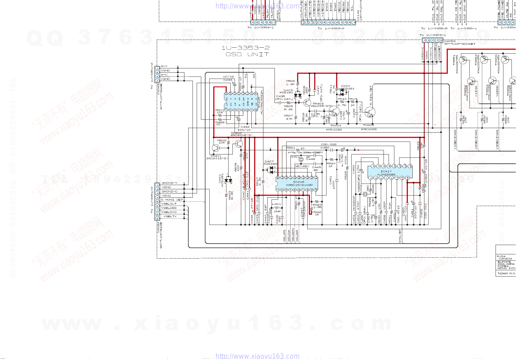
1
3
7
9
4
6
2
3
2
Q
TEL 13942296513 QQ 376315150 892498299
Q
T
E
3
L
9
6
1
5
1
5
3
1
5
2.6V
0
Q
Q
3
7
4.4V
1.8V
6
8
4.9V
0V
3
3.25V
1
9
4V
1.44V
5
1
2
3.1V
5
2.9V
2.86V
0
4
2.37V
8
9
9
2
8
5V
4
9
2
- 5V
8
2
9
9
9
9
5V
TEL 13942296513 QQ 376315150 892498299
5V 5V 5V 5V 5V
w
w
w
.
x
i
a
o
y
u
1
6
3
.
c
o
m
NOTICE
ALL RESISTANCE VALUES IN OHM. k=1,000 OHM M=1,000,000 OHM
ALL CAPACITANCE VALUES I N MICRO FARAD. P=MICRO-MICRO FARAD
EACH VOLTAGE AND CURRE NT ARE MEASUERD AT NO SIGNAL INPUT
CONDITION.
CIRCUIT AND PARTS ARE SUBJECT TO CHANGE WITHOUT PRIOR
NOTICE.
Page 97

1
3
7
9
4
6
2
3
2
Q
TEL 13942296513 QQ 376315150 892498299
5V 5V 5V 5V 5V
Q
T
E
3
L
9
6
1
5
1
5
3
1
5
0
5.1V
Q
Q
3
7
6
8
3
1
9
5
1
2
5.1V
5
0
4
5.1V
8
9
9
2
8
5.1V
4
9
2
8
2
9
9
9
9
E
TEL 13942296513 QQ 376315150 892498299
F
w
w
w
.
x
+ B LINE
- B LINE
SIGNAL LINE
WARNING:
Parts marked with this symbol have critical characteristics.
Use ONLY replacement parts recommended by the manufacture.
CAUTION:
Before returning the unit to the customer, make sure you make either (1) a
leakage current check or (2) a line to chassis resistance check. If the leakage
current exceeds 0.5 milliamps, or if the resistance from chassis to either side
of the power card is less than 460 kohms, the unit is defective.
WARNING:
i
a
DO NOT return the unit to the customer until the problem is located and
corrected.
o
y
u
1
6
3
.
SCHEMATIC DIAGRAMS (6/9)
1U-3353-1 C VIDEO & REG. UNIT
1U-3353-2 OSD UNIT
1U-3353-3 MASTER VR UNIT
1U-3353-4 AC OUTLET UNIT
1U-3353-5 P.SW UNLOCK UNIT
c
1U-3353-6 P.SW LOCK UNIT (AVC MODEL ONLY)
o
m
G
H
67
Page 98

SCHEMATIC DIAGRAMS (7/9)
1 2 3 4 5 6 7 8 9 10 11
AVR-4802/AVC-A11SR
Q
Q
3
7
6
3
1
- 14.5V
5
1
5
0
5.1V
8
2V
9
2
4
9
8
2
9
9
A
B
TEL 13942296513 QQ 376315150 892498299
T
E
L
1
3
9
4
2
2
9
6
5
1
3
- 35V
Q
Q
3
7
6
3
1
5
1
5
0
8
9
0V
2
TEL 13942296513 QQ 376315150 892498299
C
D
4
0V
9
8
2
9
9
E
w
w
w
5.1V
.
x
i
a
AC6.8V
o
y
u
NOTICE
ALL RESISTANCE VALUES IN OHM. k=1,000 OHM M=1,000,000 OHM
ALL CAPACITANCE VALUES I N MICRO FARAD. P=MICRO-MICRO FARAD
EACH VOLTAGE AND CURRE NT ARE MEASUERD AT NO SIGNAL INPUT
CONDITION.
CIRCUIT AND PARTS ARE SUBJECT TO CHANGE WITHOUT PRIOR
NOTICE.
1
6
3
.
0V
WARNING:
Parts marked with this symbol have critical characteristics.
Use ONLY replacement parts recommended by the manufacture.
CAUTION:
Before returning the unit to the customer, make sure you make either (1) a
c
leakage current check or (2) a line to chassis resistance check. If the leakage
current exceeds 0.5 milliamps, or if the resistance from chassis to either side
of the power card is less than 460 kohms, the unit is defective.
WARNING:
DO NOT return the unit to the customer until the problem is located and
corrected.
o
m
0V
+ B LINE
- B LINE
SIGNAL LINE
SCHEMATIC DIAGRAMS (7/9)
1U-3354-1 CONNECT L UNIT
1U-3354-2 CONNECT R UNIT
1U-3354-3 FLD UNIT
1U-3354-4 PHONO UNIT
1U-3354-5 PH CONNECT UNIT
1U-3354-6 232C UNIT
1U-3354-7 232C CON. UNIT
1U-3354-8 REMOTE UNIT
1U-3354-9 JOINT UNIT
F
G
H
68
Page 99

SCHEMATIC DIAGRAMS (7/9)
1 2 3 4 5 6 7 8 9 10 11
AVR-4802/AVC-A11SR
Q
Q
3
7
6
3
A
A
1
- 14.5V
5
1
5
0
5.1V
8
2V
9
2
4
9
8
2
9
9
A
B
B
B
TEL 13942296513 QQ 376315150 892498299
T
E
L
1
3
9
4
2
2
9
6
5
1
3
- 35V
Q
Q
3
7
6
3
1
5
1
5
0
8
9
0V
2
TEL 13942296513 QQ 376315150 892498299
C
D
4
0V
9
8
2
9
9
E
w
w
w
5.1V
C
C
.
x
i
a
AC6.8V
o
y
u
NOTICE
ALL RESISTANCE VALUES IN OHM. k=1,000 OHM M=1,000,000 OHM
ALL CAPACITANCE VALUES I N MICRO FARAD. P=MICRO-MICRO FARAD
EACH VOLTAGE AND CURRE NT ARE MEASUERD AT NO SIGNAL INPUT
CONDITION.
CIRCUIT AND PARTS ARE SUBJECT TO CHANGE WITHOUT PRIOR
NOTICE.
1
6
3
.
0V
D
D
WARNING:
Parts marked with this symbol have critical characteristics.
Use ONLY replacement parts recommended by the manufacture.
CAUTION:
c
Before returning the unit to the customer, make sure you make either (1) a
leakage current check or (2) a line to chassis resistance check. If the leakage
current exceeds 0.5 milliamps, or if the resistance from chassis to either side
of the power card is less than 460 kohms, the unit is defective.
WARNING:
DO NOT return the unit to the customer until the problem is located and
corrected.
o
m
0V
+ B LINE
- B LINE
SIGNAL LINE
SCHEMATIC DIAGRAMS (7/9)
1U-3354-1 CONNECT L UNIT
1U-3354-2 CONNECT R UNIT
1U-3354-3 FLD UNIT
1U-3354-4 PHONO UNIT
1U-3354-5 PH CONNECT UNIT
1U-3354-6 232C UNIT
1U-3354-7 232C CON. UNIT
1U-3354-8 REMOTE UNIT
1U-3354-9 JOINT UNIT
F
G
H
68
Page 100

Q
Q
SCHEMATIC DIAGRAMS (7/9)
1 2 3 4 5 6 7 8 9 10 11
3
7
6
3
1
5
1
5
0
8
9
2
4
9
8
2
9
9
TEL 13942296513 QQ 376315150 892498299
T
E
L
1
3
9
4
2
2
9
6
5
1
3
Q
Q
3
7
6
3
1
- 14.5V
5
1
5
0
8
9
2
4
9
8
2
9
TEL 13942296513 QQ 376315150 892498299
5.1V
9
w
w
w
.
x
i
a
o
y
u
1
6
3
.
c
o
m
 Loading...