

Denon AVR-2802, AVR-2982 Service Manual

Hi-Fi Component
SERVICE MANUAL
MODEL
AVR-2802/982
AV SURROUND RECEIVER
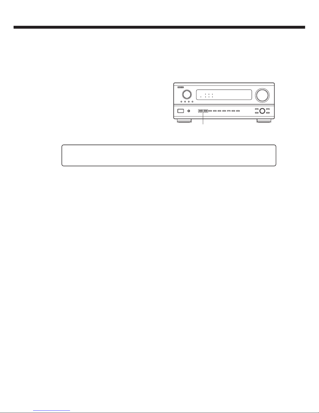
Some illustrations using in this service manual are slightly different from the actual set.
For U.S.A., Canada, Europe,
Asia, China, Hong Kong &
Taiwan R.O.C. model
X0119 1174 NC 0112
14-14, AKASAKA 4-CHOME, MINATO-KU, TOKYO 107-8011 JAPAN
Telephone: 03 (3584) 8111

2
AVR-2802/982
SPECIFICATIONS
AUDIO SECTION
Power Amplifier
Rated output: Front: 90W + 90W (8Ω/ohms, 20Hz ~ 20kHz with 0.05% T.H.D.)
135W + 135W (6Ω/ohms, 1kHz with 0.7% T.H.D.)
150W + 150W (6Ω/ohms, EIAJ)
Center: 90W (8Ω/ohms, 20Hz ~ 20kHz with 0.05% T.H.D.)
135W (6Ω/ohms, 1kHz with 0.7% T.H.D.)
150W (6Ω/ohms, EIAJ)
Surround: 90W + 90W (8Ω/ohms, 20Hz ~ 20kHz with 0.05% T.H.D.)
135W + 135W (6Ω/ohms, 1kHz with 0.7% T.H.D.)
150W + 150W (6Ω/ohms, EIAJ)
Surround Back: 90W (8Ω/ohms, 20 Hz ~ 20kHz with 0.05% T.H.D.)
135W (6Ω/ohms, 1kHz with 0.7% T.H.D.)
150W (6Ω/ohms, EIAJ)
Dynamic power: 120W × 2ch (8Ω/ohms)
170W × 2ch (4Ω/ohms)
200W × 2ch (2Ω/ohms)
Output terminals: Front: A or B 6 ~ 16Ω/ohms
A + B 8 ~ 16Ω/ohms
Center, Surround, Surr.Back: 6 ~ 16Ω/ohms
Analog
Input sensitivity/input impedance: 200mV/47kΩ/kohms
Frequency response: 10Hz ~ 100kHz: +0, −3dB (DIRECT mode)
S/N: 102dB (DIRECT mode)
Distortion: 0.005% (20Hz ~ 20kHz) (DIRECT mode)
Rated output: 1.2V
Digital
D/A output: Rated output 2V (at 0dB playback)
Total harmonic distortion 0.008% (1 kHz, at 0 dB)
S/N ratio 102dB
Dynamic range 96dB
Digital input: Format Digital audio interface
Phono equalizer (PHONO input
REC OUT)
Input sensitivity: 2.5mV
RIAA deviation: ±1dB (20Hz to 20kHz)
Signal-to-noise ratio: 74dB (A weighting, with 5mV input)
Rated output/Maximum output: 150mV/7V
Distortion factor: 0.03% (1kHz, 3V)
VIDEO SECTION
Standard video jacks
Input/output level and impedance: 1Vp-p, 75Ω/ohms
Frequency response: 5Hz ~ 10MHz +0, −3dB
S-video jacks
Input/output level and impedance: Y (brightness) signal 1Vp-p, 75Ω/ohms
C (color) signal 0.286Vp-p, 75Ω/ohms
Frequency response: 5Hz ~ 10MHz +0, −3dB
Color component video jacks
Input/output level and impedance: Y (brightness) signal 1Vp-p, 75Ω/ohms
PB/CB (blue) signal 0.7Vp-p, 75Ω/ohms
PR/CR (red) signal 0.7Vp-p, 75Ω/ohms
Frequency response: 5Hz ~27MHz +0, −3dB
TUNER SECTION
[FM] (note: µV at 75Ω/ohms, 0dBf=1 × 10
-15
W) [AM]
Receiving Range: 87.50MHz ~ 107.90MHz 520kHz ~ 1710kHz
(for U.S.A., Canada and multiple voltage models) (for U.S.A., Canada and Multiple voltage models)
87.50MHz ~ 108.00MHz 522kHz ~ 1611kHz
(for Europe, Asia, China, Hong Kong, Taiwan R.O.C. and Multiple voltage models) (for Europe, Asia, China, Hong Kong, Taiwan R.O.C. and multiple voltage models)
Usable Sensitivity: 1.0µV (11.2dBf) 18µV
50dB Quieting Sensitivity: MONO: 1.6µV (15.3dBf)
STEREO: 23µV (38.5dBf)
S/N (IHF-A): MONO: 77dB
STEREO: 72dB
Total Harmonic Distortion (at 1kHz): MONO: 0.15%
STEREO: 0.3%
GENERAL
Power supply: AC120V, 60Hz (for U.S.A., Canada and Taiwan R.O.C. models)
AC230V, 50Hz (for Europe model)
AC220V, 50Hz (for China model)
AC115V/230V, 50/60Hz (for Asia, Hong Kong and Multiple voltage models)
Power consumption: 5.0A (for U.S.A.& Canada model)
270W (for Europe, Asia, China, Hong Kong and Multiple voltage models)
650W (for Taiwan R.O.C. model)
2.0W Max (Standby)
Maximum external dimensions: 434 (W) × 171 (H) × 416 (D)mm (17-3/32″ × 6-11/32″ × 16-3/8″)
Weight: 11.5kg (25 lbs 6 oz)
REMOTE CONTROL UNIT (RC-903: for U.S.A., Canada, Asia, China, Hong Kong, Taiwan R.O.C. and Multiple voltage models)
(RC-904: for Europe model)
Batteries: R6P/AA Type (three batteries)
External dimensions: 70 (W) × 215 (H) × 24 (D)mm (2-3/4″ × 8-15/32″ × 15/16″)
Weight: 200g (Approx. 7 oz) (including batteries)
* For purposes of improvement, specifications and design are subject to change without notice.
SAFETY PRECAUTIONS
The following check should be performed for the continued protection of the customer and service technician.
LEAKAGE CURRENT CHECK
Before returning the unit to the customer, make sure you make either (1) a leakage current check or (2) a line to chassis
resistance check. If the leakage current exceeds 0.5 milliamps, or if the resistance from chassis to either side of the
power cord is less than 460 kohms, the unit is defective.

3
AVR-2802/982
WIRE ARRANGEMENT
If wire bundles are untied or moved to perform adjustment or parts replacement etc.,be sure to rearrange them neatly as they
were originally bundled or placed afterward.
Otherwise, incorrect arrangement can be a cause of noise generation.
Wire arrangement viewed from the top

4
AVR-2802/982
DISASSEMBLY
(Follow the procedure below in reverse order when reassembling)
1. Top Cover
Remove 3 screws 1 on the rear and 6 screws 2 on both
sides to detach the Top Cover as shown in the arrow
direction.
2. Front Panel
(1) Remove 7 screws 3 from the top and bottom edges of
the Front Panel.
(2) Release 4 top and bottom hooks, then detach the Front
Panel as shown in the arrow direction.
Top Cover
3. Inner Panel
Pull out the Inner Panel in the arrow direction after removing
3 screws
4
.
Inner Panel
Hook
2
2
1
3
3
3
Hook
Hook
Hook
Front Panel
4
4
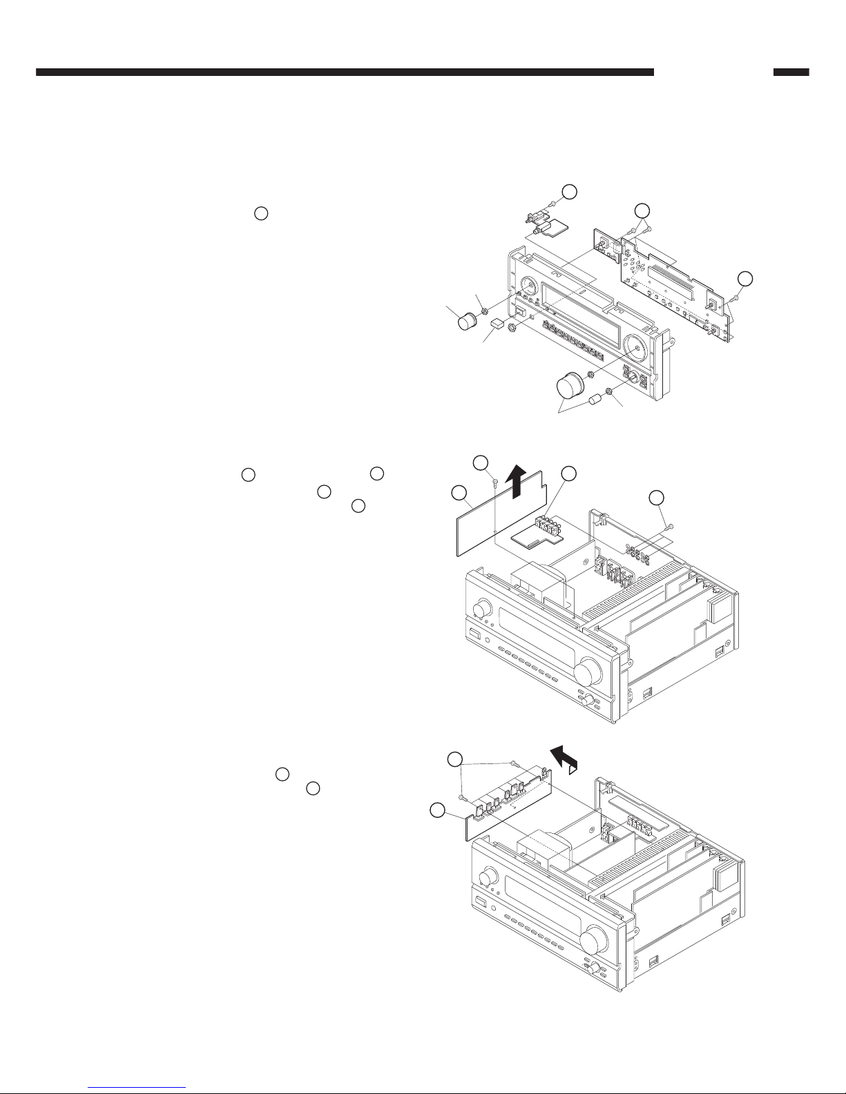
5
AVR-2802/982
4. Inner Panel Ass'y
(1) Remove 3 round and 1 square knobs, and unscrew 4
nuts.
(2)Remove 15 screws
5
fixing each P.W.B.
Round Knob
5
5
5
Nut
Square Knob
Round Knob
Nut
5. Amp Connect Unit
(1) Remove 3 screw to detach Pre-out Unit .
(2) Take off the Amp Connect Unit as shown in the
arrow direction after removing 1 screw .
6
7
8
9
1 0
6. Regulator Unit
Take off the Regulator Unit as shown in the arrow
direction after removing 9 screws .
1 1
6
7
8
9
1 0
1 1

6
AVR-2802/982
7. Component-Video/S-Video / C-video /
Audio & DSP / Ext-in VR / Digital-in / AM
FM Tuner Unit
(1) Remove 44 screws to detach the Rear Panel.
(2) Take off the objective P.W.B. upward.
1 3
8. How to Check Power / Control Unit with
Power-on
(1) Remove 13 screws ,and 4 screws fixing to the
Chassis.
(2) Pull up the Unit to separate from the Chassis.
1 2
1 2
1 2
1 2
Rear Panel
1 4
1 3
1 3
1 3
1 3
1 3
1 3
1 4
1 4
AVR-2802/982
7
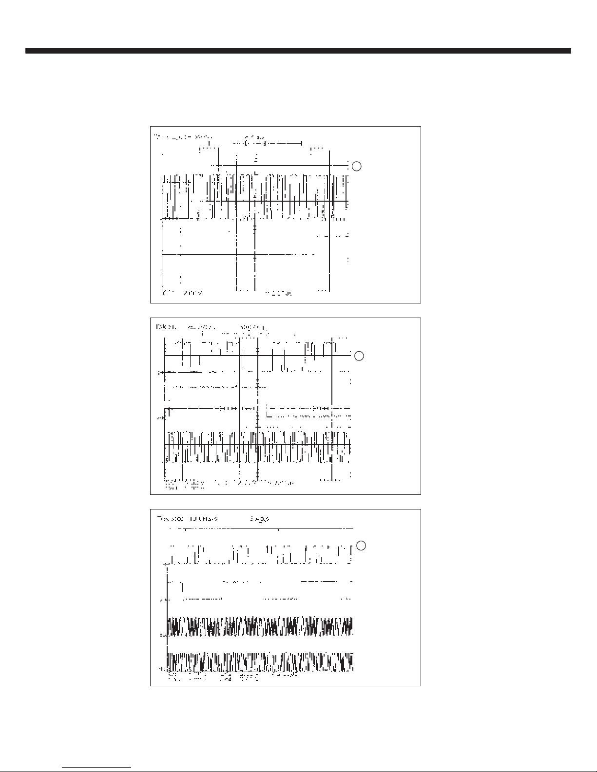
CLOCK FLOW & WAVE FORM IN DIGITAL BLOCK
Wave Form
CH1: D-DATA
(IC505 (5) )
1
CH1: DATA
CH2: fs
CH3: 64fs
CH4: 256fs
3
CH1: DATA
CH2: DA-LRCK(fs)
CH3: DA-SCK(64fs)
2

AVR-2802/982
8
A/D SELECTOR
IC804
74LVX157
CODEC
D/A CONVERTER
IC801
AD1854
(2)256fs
(26)64fs
(25)fs
(27)DATA
INPUT
SELECTOR
IC505
151NS
COAXIAL
(15)
OPTICAL-1
OPTICAL-2
OPTICAL-3
(14)
(5)
(13)
OPTICAL
OUTPUT
(12)
IC506
151NS
(3)
(5)
(2)
(1)
IC800
LC89055W
CKOUT(13)
(5)DIN2
BCK
DATA
(14)
LRCK(15)
(16)
XIN(22)
XMCK(20)
12.288MHz
X801
MCLK
(44) (22) (25) (26)
SCLKN1 LRCKN1
SDATAN1
AUDATA0(41)
AUDATA1(40)
AUDATA2(39)
(30)CLKIN
IC814
CS493292
DSP
2
1
(27) (43) (42)
SCLK LRCLKCMPDAT
3
MCLK
DA SCK
DA LRCK
SD IN
256fs
64fs
fs
FRONT
SURROUND
256fs
64fs
fs
DATA
IC813
(7)
(13)
(10)
SN74LV4040APW
DIR
(6)SDTI1
IC602
AK4527
(7)SDTI2
(8)SDTI3
(39)MCLK
(4)BICK
(5)LRCK
(9)SDTO
XMT958 (3)
SURROUND BACK
CENTER/SW
SN74HC
SN74HC
* fs is a sampling frequency of input digital signal.
e.g.:sampling frequency 48kHz fs=48kHz
* 64fs and 256fs are 64 or 256 times the sampling frequency respectively.
e.g.: sampling frequency 48kHz
64fs: 48kHz x 64=3.072MHz
256fs: 48kHz x 256=12.288MHz
* The sampling frequency for analog input is fixed to 48kHz internally.
* (No.) indicates the pin number of individual.
* The arrow indicates the direction of signal as the input terminal pointed by
the arrow and the output terminal by the opposite.
Clock Flow

8
76
5
4
3
2
1
A
B
C
D
E
BLOCK DIAGRAM
AVR-2802/982
9

8
76
5
4
3
2
1
A
B
C
D
E
LEVEL DIAGRAMS (1/3)
AVR-2802/982
10
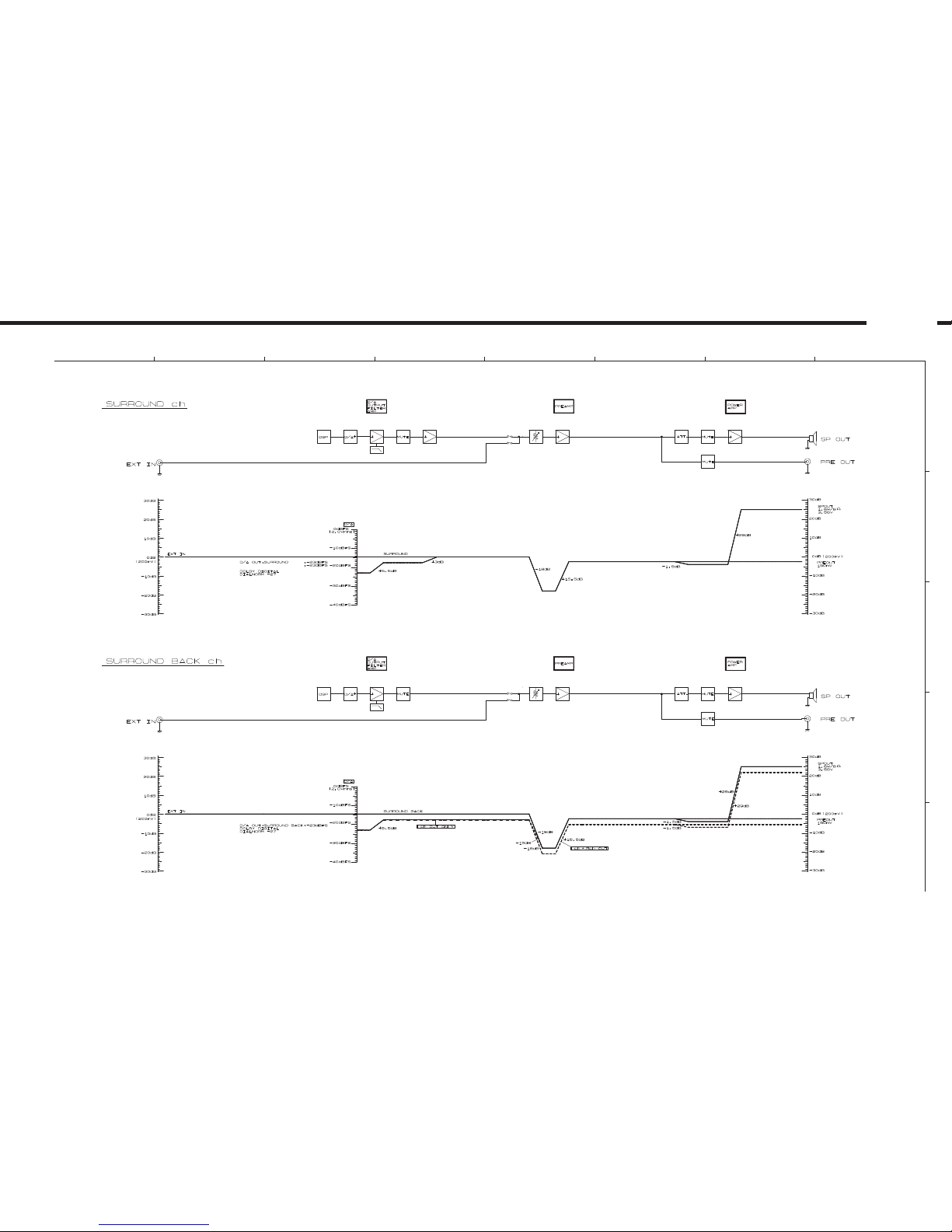
8
76
5
4
3
2
1
A
B
C
D
E
LEVEL DIAGRAMS (2/3)
AVR-2802/982
11
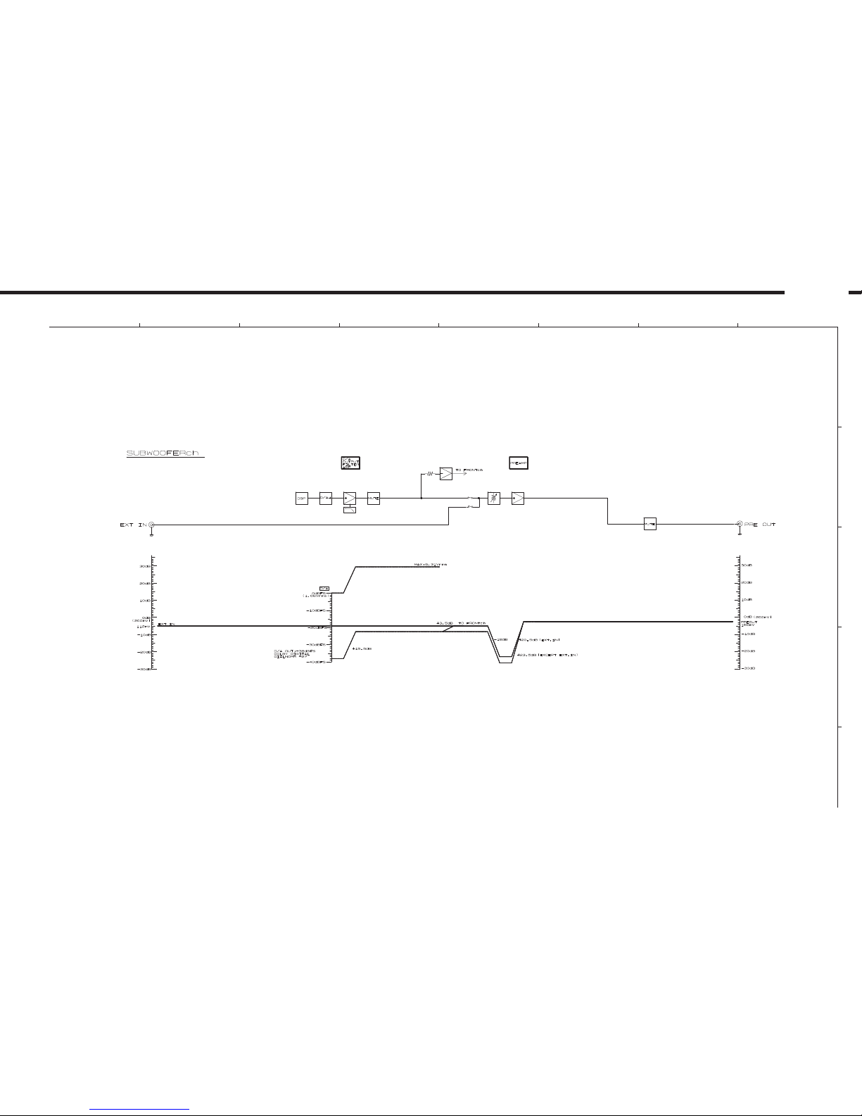
8
76
5
4
3
2
1
A
B
C
D
E
LEVEL DIAGRAMS (3/3)
AVR-2802/982
12
AVR-2802/982
13
CAUTION IN SERVICING
Initializing AV SURROUND RECEIVER
AV SURROUND RECEIVER initialization should be performed when the µcom, peripheral parts of µcom, and DSP
P.W.B. are replaced.
1. Switch off the unit and remove the AC cord from the
wall outlet.
2. Hold the following A button and B button, and plug
the AC cord into the outlet.
3. Check that the entire display is flashing with an
interval of about 1 second, and release your fingers
from the 2 buttons and the microprocessor will be
initialized.
Note: If step 3 does not work, start over from step 1.
All user settings will be lost and its factory setting will be recovered when this initialization mode.
So make sure to memorize your setting for restoring after the initialization.
2
VOLUME LEVEL
AUTO
LOCK
STAND BY
DIGITAL
PCM
SIGNAL
DIGITAL
INPUT
REMOTE
SENSOR
14
AVR-2802/982
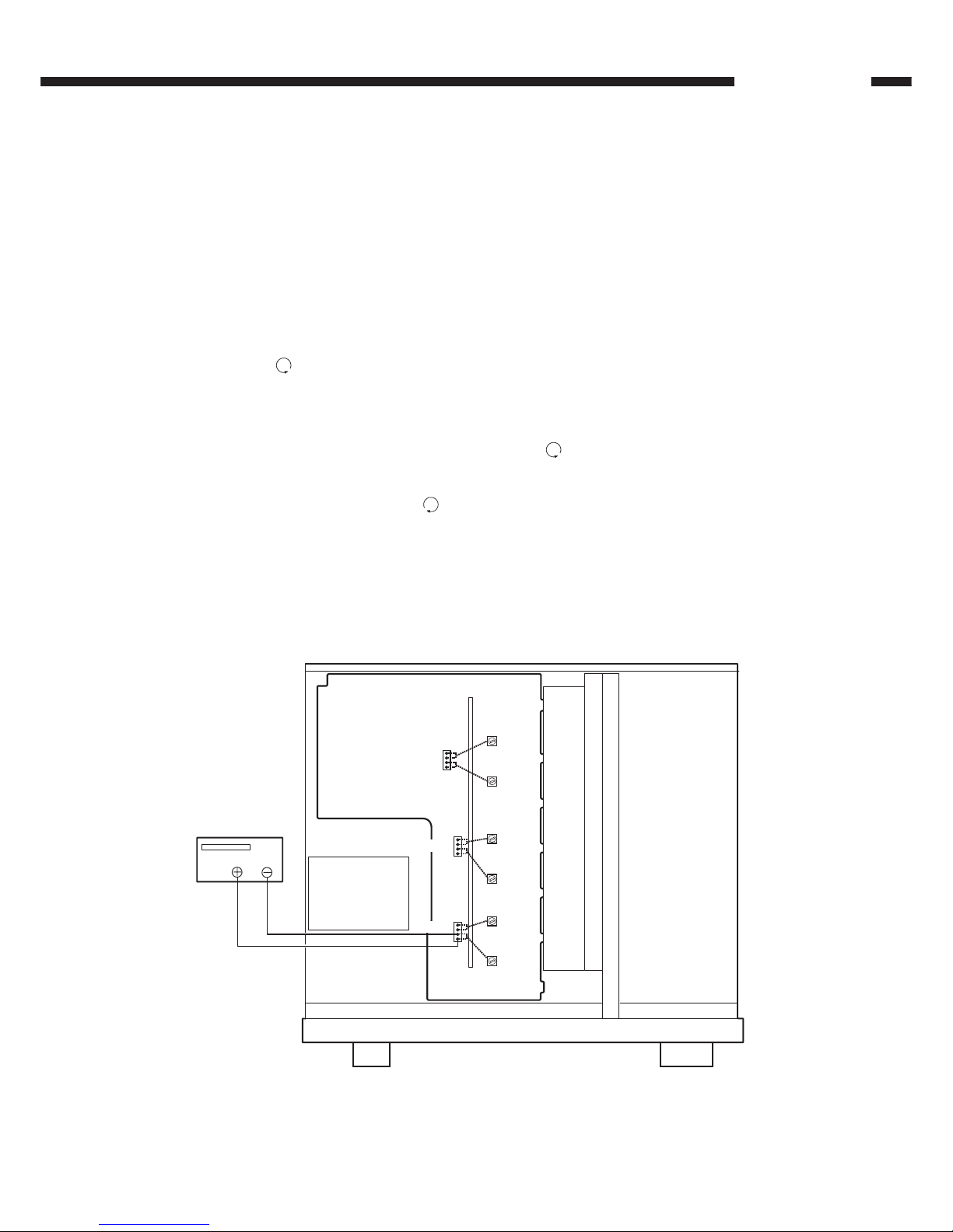
ADJUSTMENT
Idling Current (1U-3368-1)
Required measurement equipment : DC Voltmeter
Preparation
(1) Avoid direct blow from an air conditioner or an electric fan, and adjust the unit at normal room tempereture 15 °C ~ 30 °C
(59 °F ~ 86 °F).
(2) Presetting
POWER (Power sourse switch) → OFF
SPEAKER (Speaker terminal) → No load (Do not connect speaker, dummy resistor, etc.)
Adjustment
(1) Remove top cover and set VR101, VR102, VR201, VR202, VR301, VR401, on 1U-3368-1 (Power Unit) at fully
counterclockwise (
).
(2) Connect DC Voltmeter to test points (FRONT-Lch: TP101, FRONT-Rch: TP102, CENTER ch: TP103, SURROUND-Lch:
TP101, SURROUND-Rch: TP103, SURROUND BACK-ch: TP102).
(3) Connect power cord to AC Line, and turn power switch "ON".
(4) Presetting. MASTER VOLUME : "---" counterclockwise (
min.)
MODE : 6CH STEREO
FUNCTION : CD
(5) Allow 2 minutes, and turn VR101 clockwise ( ) to adjust the TEST POINT voltage to 6.5 mV ±0.5 mV DC.
(6) After 10 minutes from preset, turn VR101 to set the voltage to 8 mV ±0.5 mV DC.
(7) Adjust the Variable Resistors of other channels in the same way.
(8) After 5 minutes from (6), turn VR101 to set the voltage to 8 mV ±0.5 mV DC.
(9) Adjust the Variable Resistors of other channels in the same way.
TP102
VR301
VR102
VR401
VR202
VR101
VR201
SRch
SBch
FRch
Cch
FLch
SLch
DC Voltmeter
TP103
TP101
15
AVR-2802/982
Name
Function
TMP88CU74F Terminal Function
Pin
No.
1 P02/S01 RDS RESET O C Z L RDS reset output (LC72720)
2 P03 OSD RST O C Z H OSD control output (M35015)
3 P04 PLL DATA I PLL Serial data input terminal (LC72131)
4 P05 PLFLRDS DATA O C Z L
PLL, FL, RDS control terminal (LC72131 & LC75721, LC72720)
5 P06 PLL STB O C Z L PLL control terminal (LC72131)
6 P07 PLFLRDS CLK O C Z L
PLL, FL, RDS control terminal (LC72131 & LC75721, LC72720)
7 Vss Vss I GND L GND
8 Xout Xout O XTAL
9 Xin Xin I XTAL
10 RESET_ RESET_ I Eu Lv L Reset input
11 P22/XTOUT TUNED_ I Eu Lv Z Tuning detect, L: Tuned
12 P21/XTIN STEREO_ I Eu Lv Z L: At stereo receive
13 TEST TEST I GND S Connect to GND
14 P20/INT5_ B.DOWN_ I Eu Lv Z Power down detect, L: Power down
15 P10/INT0_ PROTECT_ I Ed E&L Z PROTECTION detect input, H: Detect
16 P11/INT1 RDS DATA I Z L RDS data input (LC72720)
17 P12 OSD CLK O C Z H OSD control output (M35015)
18 P13 OSD CS O C Z H OSD control output (M35015)
19 P14 OSD DATA O C Z L OSD control output (M35015)
20 P15/INT3 REMOCON I Ed E&L Z Remote control signal input
21 P16/INT2 ACK O C Z L MAIN-SUB CPU comm. control terminal
22 P17/INT4 REQ I Eu Z L MAIN-SUB CPU comm. control terminal
23 P30/SCL SI I MAIN-SUB CPU comm. control terminal
24 P31/SDA SO O C MAIN-SUB CPU comm. control terminal
25 P32/SCK0_ CLK O C MAIN-SUB CPU comm. control terminal
26 P40/AIN0 MODE I Eu Lv Z Destination switching input
27 P41/AIN1 KEY1 I Eu Lv Z Button input 1
28 P42/AIN2 KEY2 I Eu Lv Z Button input 2
29 P43/AIN3 KEY3 I Eu Lv Z Button input 3
30 P44/AIN4 FUNC STB1 O C Z L
Function control output, REC OUT (TC9274-011), EXT/SOURCE (TC9274-017)
31 P45/AIN5 FUNC/T. CON CLK O C Z L
Function control output (TC9274N, TC9273), TONE control output (TC9184P)
32 P46/AIN6 FUNC/T. CON DATA O C Z L
Function control output (TC9274N, TC9273), TONE control output (TC9184P)
33 P47/AIN7 E.VOL STB4 O C Z L Elect. volume control output (TC9482)
34 P50/AIN8 E.VOL STB1 O C L L Elect. volume control output (TC9459)
35 P51/AIN9 TONE STB O C L L TONE control output (TC9184P)
36 P52/AIN10 E.VOL DATA O C L H Elect. volume control output (TC9459, TC9482)
37 P53/AIN11 E.VOL CLK O C L H Elect. volume control output (TC9459, TC9482)
Symbol I/O Type Op Det Res Init
SEMICONDUCTORS
IC’s
Note: Abbreviation ahead of IC No. indicates the name of P.W.B.
PO: Power P.W.B. RE: Regulator P.W.B.
EX: Exit in P.W.B. AU: Audio/DSP P.W.B.
CO: Control P.W.B.
TMP88CU74F
(CO: IC303)
Function
38 VASS VASS I Ref. volt (GND)
39 VAREF VAREF I Ref. volt (VDD)
40 VDD VDD I Power supply
41 P60 FL CE O P Ed S L H FL display control output (LC75721NE)
42 P61 FL RES O P Ed S L H FL display control output (LC75721NE)
43 P62 FUNC STB2 O P Ed Z L Function control output (TC9273), INPUT (TC9273)
44 P63 FA-RELAY O P Id L L Front SP relay A control terminal, L: Mute
45 P64 FB-RELAY O P Id L L Front SP relay B control terminal, L: Mute
46 P65 C-RELAY O P Id L L Center SP relay control terminal, L: Mute
47 P66 S-RELAY O P Id L H Surround SP relay control terminal, L: Mute
48 P67 PRE F MUTE O P Ed L H Front PRE OUT mute control terminal, L: Mute
49 P70 PRE C MUTE O P Ed L L Center PRE OUT mute control terminal, L: Mute
50 P71 PRE S MUTE O P Ed L L Surround PRE OUT mute control terminal, L: Mute
51 P72
SUB WOOFER MUTE
O P Ed L H Sub-woofer PRE OUT mute control terminal, L: Mute
52 P73 H/P RELAY O P Id L H H/P OUT relay control terminal, L: Mute
53 P74 EXP OE O P Ed L H Port expander control terminal (BU4094)
54 P75 EXP CLK O P Ed L L Port expander control terminal (BU4094)
55 P76 EXP DATA O P Ed L L Port expander control terminal (BU4094)
56 P77 EXP STB O P Ed L L Port expander control terminal (BU4094)
57 P80 POWER O P Id L H Power relay control output, H: ON
58 P81 RESET2 O P Id L L Reset signal output to sub-CPU, H: Reset
59 P82 PRE S.BACK MUTE O P Id L L Surround Back PRE PUT mute control terminal, L: Mute
60 P83 S.BACK VOL MUTE O P Id L L Surround Back volume mute, L: Mute
61 P84 STANDBY O P Id L H Standby LED drive output H: Light
62 P85 S.BACK RELAY O P Id L L Surround Back SP relay control terminal, L: Mute
63 P86 LED CK O P Id L L LED control terminal (BU2090F)
64 P87 LED DATA O P Id L L LED control terminal (BU2090F)
65 P90 TUNER MUTE O P Ed L H TUNER mute control terminal, L: Mute
66 P91 MULTI MUTE O P Id L H MULTI PREOUT mute control terminal, L: Mute
67 P92 S MONI DET I Eu Lv Z S monitor connection detect input, L: Connected
68 P93 S SIG DET I Eu Lv Z S signal detect input, H: Detected
69 P94 SYNC DET. I Eu Lv Z Sync detect input, H: Ext. sync
70 P95 SEL A (M) I Eu Lv Z Master volume rotation detect input (rotary encoder)
71 P96 SEL B (M) I Eu Lv Z Master volume rotation detect input (rotary encoder)
72 P97 CINEMA EQ O P Eu Lv Z L CINEMA EQ control output, H: ON
73 PD0 VOL MUTE O P Ed L L Master volume minimum control, L: Min.
74 PD1 SEL C (S) I Eu Lv Z Surround mode rotation detect input (rotary encoder)
75 PD2 SEL D (S) I Eu Lv Z Surround mode rotation detect input (rotary encoder)
76 PD3 SEL E (F) I Eu Lv Z
Input selector switch rotation detect input (rotary encoder)
77 PD4 SEL F (F) I Eu Lv Z
Input selector switch rotation detect input (rotary encoder)
78 Vkk Vkk GND fixed
79 P00/SCK1_ O C Z L
80 P01/SI1 RDS CE O C Z L RDS data output (LC72720)
I/O Type Op Det Res Init
Name
Pin
No.
Symbol
1 24
25
40
41
64
65
80
NOTE:
Pin No. :Terminal number of microcomputer.
Port Name : The name entered in the data sheet of microcomputer.
Symbol :Symbolized interface function.
I/O : Input or out of part.
“I” = Input port
“O” = Output port
Type :Composition of port in case of output port.
“C” = CMOS output
“N” = NMOS open drain output
“P” = PMOS open drain output
Op : Pull up/Pull down selection information.
“Iu” = Inner microcomputer pull up
“Id” = Inner microcomputer pull down
“Eu” = External microcomputer pull up
“Ed” = External microcomputer pull down
Det :Indicates judging state of input port. Level detection is “LV”; Edge detection is “Ed”;
Detection by both shifting is “E&L”; Serial data detection is “S” (Serial data output is also “S”).
Res : State at reset.
“H” = Outputs High Level at reset
“L” = Outputs Low Level at reset
“Z” = Becomes High impedance mode at reset
Ini : Initial output state.
Function :Function and logical level explanation of signals to be interface.
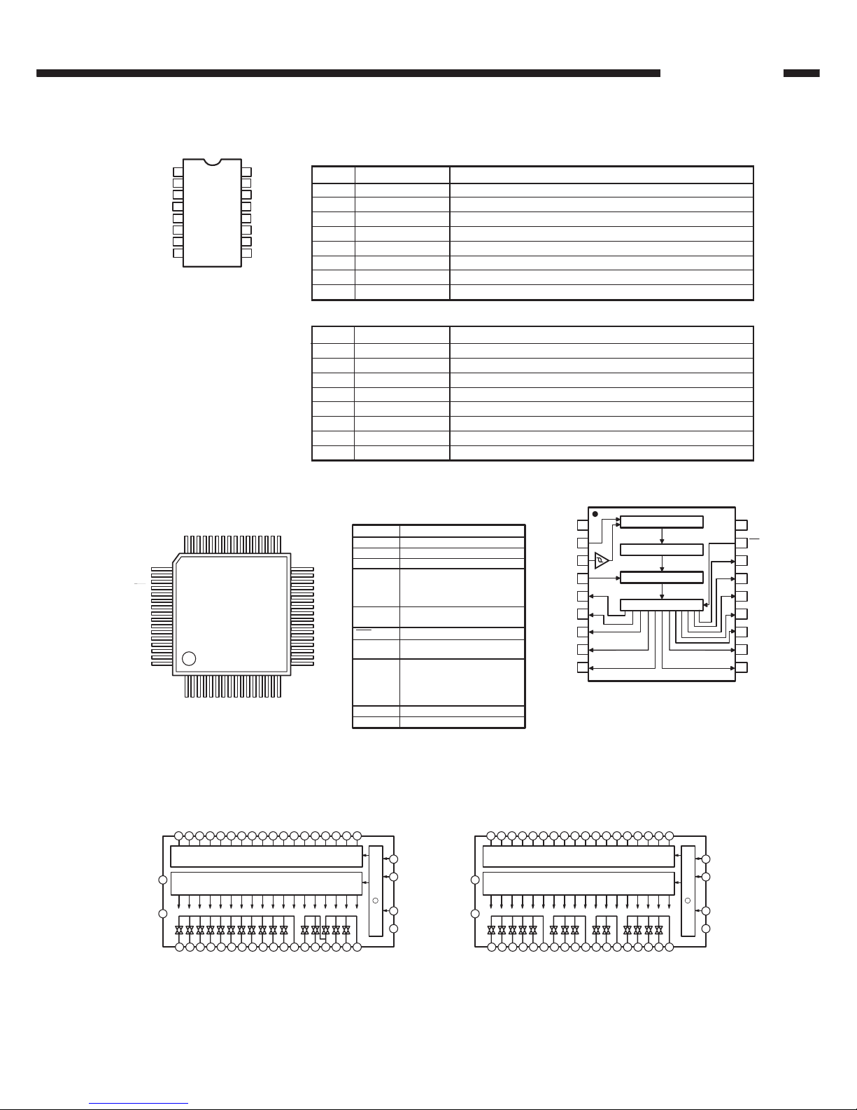
TMP93CS40F (AU: IC301)
Name
Function
TMP93CS40F Terminal Function
Pin
No.
1 V REFL A/D ref. GND
2 A Vss ← A/D GND
3 A Vcc ← AD +5V
4 _NMI I Not used (fixed to H)
5 P70/TI0 C15 O C Ed L L Fixed to L (DSP ROM address cont. out bit 15, not used)
6 P71/TO1 C16 O C Ed L L DSP program ROM address cont. out bit 16
7 P72/TO2 C17 O C Ed L L DSP program ROM address cont. out bit 17
8 P73/TO3 ROM/RAM O C Ed L L ROM/RAM switching control terminal (L:ROM)
9 P80/INT4/TI4 _INTREQ OUT I/O C Eu E↓&L Z DSP request input and cont. output (L:Rq & cont.)
10 P81/INT5/TI5 B.DOWN I Eu E↑&L Z Power down detect (H: Detected)
11 P82/TO4 O C L L
12 P83/TO5 _REQ O C Eu H L
MAIN-SUB CPU comm. control output (L: Comm. request from
sub)
13 P84/INT6/TI6 _ACK I Eu E↓&L MAIN-SUB CPU comm. control input (L: Ack. return from main)
14 P85/INT7/TI7 ERR I E↑&L DIR control input terminal (LC89055Q)( H: ERR)
15 P86/TO6 I Lv Z (GND)
16 P97/INT0 _CS I Ed E↑&L
DIR control input terminal (LC89055Q), when CH status change
L→H
17 P90/TXD0 SI O C MAIN-SUB CPU comm. control terminal (data output)
18 P91/RXD0 SO I MAIN-SUB CPU comm. control terminal (data input)
19
P92/_CTS0/SCLK0
CLK I/O C MAIN-SUB CPU comm. control terminal (I2C clock in/output)
20 P93/TXD1 O C Z L
21 P94/RXD1 O C Z L
22 P95/SCLK1 O C Z L
23 AM8/_16 ← Fixed to +5V
24 CLK O C Eu
25 Vcc ← +5V
26 Vss I/O1 GND
27 X1 Xin I X′tal connection
28 X2 Xout O X′tal connection
29 _EA ← Fixed to +5V
30 _RESET RESET2_ I Eu Lv L Reset input (controlled by main CPU)
31 P96/XT1 A/D RESET O N Eu H H A/D control terminal (L: Reset)
32 P97/XT2 O C Ed L L
33 TEST1 ← I Connected to TEST2
34 TEST2 ← I Connected to TEST1
35 PA0 DINA O C Ed L L Digital input switching control output
36 PA1 DINB O C Ed L L Digital input switching control output
37 PA2 O C L L
38 PA3 DINC O C Ed L L Digital input switching control output
39 PA4 DOUTA O C Ed L L Digital output switching control output
40 PA5 DOUTB O C Ed L L Digital output switching control output
Symbol
I/O Type Op Det Res Init
Name
Function
Pin
No.
41 PA6 DEEMP O C Ed L L DAC de-emphasis filter cont. out terminal (H:ON)
42 PA7/SCOUT 96k-DAC O C L L DAC control terminal (H: Sample frequency 96kHz)
43 ALE O C L L (Address latch enable)
44 Vcc +5V
45 P00/AD0 (AD0) I/O C Z L (EPROM data in D0 / address out A0)
46 P01/AD1 (AD1)) I/O C Z L (EPROM data in D1 / address out A1)
47 P02/AD2 (AD2) I/O C Z L (EPROM data in D2 / address out A2)
48 P03/AD3 (AD3) I/O C Z L (EPROM data in D3 / address out A3)
49 P04/AD4 (AD4) I/O C Z L (EPROM data in D4 / address out A4)
50 P05/AD5 (AD5) I/O C Z L (EPROM data in D5 / address out A5)
51 P06/AD6 (AD6) I/O C Z L (EPROM data in D6 / address out A6)
52 P07/AD7 (AD7) I/O C Z L (EPROM data in D7 / address out A7)
53 P10/AD8/A8 (A8) O C Z L (EPROM address out A8)
54 P11/AD9/A9 (A9) O C Z L (EPROM address out A9)
55 P12/AD10/A10 (A10) O C Z L (EPROM address out A10)
56 P13/AD11/A11 (A11) O C Z L (EPROM address out A11)
57 P14/AD12/A12 (A12) O C Z L (EPROM address out A12)
58 P15/AD13/A13 (A13) O C Z L (EPROM address out A13)
59 P16/AD14/A14 (A14) O C Z L (EPROM address out A14)
60 P17/AD15/A15 (A15) O C Z L (EPROM address out A15)
61 _WDTOUT ← O C Z H Watch dog output
62 Vss ← GND
63 Vcc ← +5V
64 P20/A0/A16 (A16) O C Z L (EPROM address out A16)
65 P21/A1/A17 DIR CLK O C Z L DIR control terminal (LC89055Q) control clock output
66 P22/A2/A18 DIR CE O C Z L DIR control terminal (LC89055Q) control chip enable output
67 P23/A3/A19 DIR MOSI O C Z L DIR control terminal (LC89055Q) control data output
68 P24/A4/A20 DIR MOSO I Lv DIR control terminal (LC89055Q) control data input
69 P25/A5/A21 FGAIN O C Ed L L FRONT ch GAIN switching control output (H: SW=NO)
70 P26/A6/A22 DAC-RESET O C Ed L H
DAC control terminal (L: Power down mode, ↑(rising edge) Reset)
71 P27/A7/A23 SEL CK O C Z L ADC/DIR data clock switching control terminal (L: ADC)
72 P30/_RD (_RD) O C Z L (Flash memory control terminal)
73 P31/_WR (_WR) O C Z L (Flash memory control terminal)
74 P32/_HWR CSI I Lv DIR control input terminal (L: PCM)
75 P33/_WAIT ERR MUTE_ O C Ed L L Pop noise preventive mute control output (L: Mute)
76 P34/_BUSRQ I Lv Z GND
77 P35/_BUSRQ DIG.(AC3) MUTE O C Ed Z L Digital mute control output (L: AC-3 or DTS decode enable)
78 P36/_R/W I Lv Z GND
79 P37/_RAS DIR RESET O C Z L DIR control output (LC89055Q) (L: Reset)
80
P40/_CS0/_CAS0
O C Z L
81
P41/_ CS1/_CAS1
O C Z L
82
P42/_ CS2/_CAS2
(_CS0) O C Z L (Flash memory control terminal)
83 P60/PG00 DSP. RESET O C Z L DSP reset output terminal (L:Reset)
84 P61/PG01 I/02 SCD OUT I C Lv Z DSP status data input terminal
85 P62/PG02 I/03 DSP. CS O Z L DSP chip select cont.output (L:Data out)
86 P63/PG03 I/04 DSP. CLK O C Z L DSP data clock output terminal
87 P64/PG10 I/05 SCD IN O C Z L DSP data output terminal
88 P65/PG11 I/06 4527_CE O C Z L AD control terminal (AK4527), Chip enable output
89 P66/PG12 I/07 4527_CLK O C Z L AD control terminal (AK4527), Data clock output
90 P67/PG13 I/08 4527_DIN O C Z L AD control terminal (AK4527), Data output
91 Vss ← GND
92 P50/AN0 INTTREQ IN I Eu Lv Z
93 P51/AN1 I Eu Lv Z
94 P52/AN2 EMP I Lv H: EMP on
95 P53/AN3 96K DET I Lv 96k signal detect input, H: 96k
96 P54/AN4 I Eu Lv Z
97 P55/AN5 I Eu Lv Z
98 P56/AN6 ACC ON/OFF I Eu Lv Z
99 P57/AN7 I Eu Lv Z
100 V REFH ← AD ref. +5V
Symbol
I/O Type Op Det Res Init
7 5
7 6
1 0 0
1
2 5
2 6
5 0
5 1
16
AVR-2802/982
AVR-2802/982
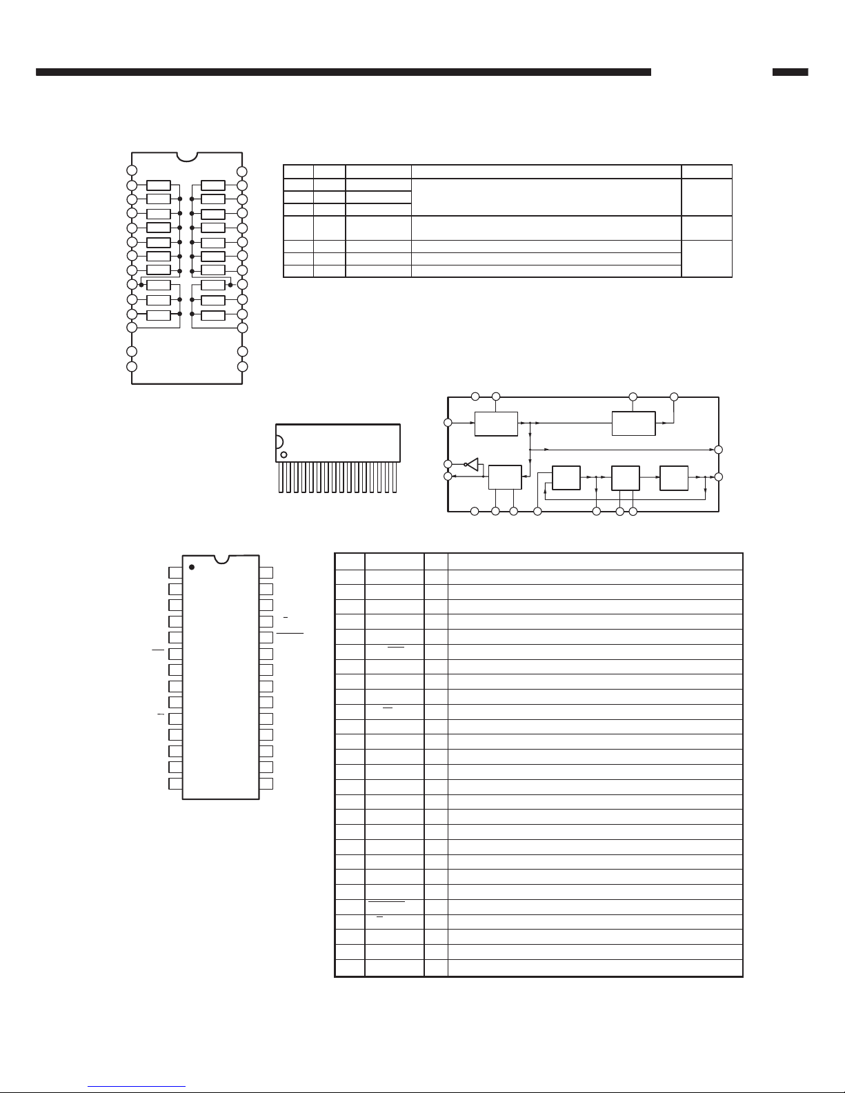
17
1,12,23 VD1,2,3 Digital power supply (+)
2,13,24 DGND1,2,3 Digital GND
3 AUDATA3, XMT958 SPDIF transmitter output, Digital audio output 3
4 WR, DS, EMWR, GPIO10
Host write strobe, Host data strobe, External memory write enable,
General purpose in/output 10
5 RD, R/W, EMOE,GPIO11
Host parallel output enable, Host parallel R/W, External memory write enable,
General purpose in/output 11
6 A1,SCDIN Host address bit 1, SPI serial control data input
7 A0,SCCLK Host address bit 0, Serial control port clock
8 DATA7, EMAD7, GPIO7 Bidirectional data bus 7, External memory address 7, General purpose in/output 7
9 DATA6, EMAD6, GPIO6 Bidirectional data bus 6, External memory address 6, General purpose in/output 6
10 DATA5, EMAD5, GPIO5 Bidirectional data bus 5, External memory address 5, General purpose in/output 5
11 DATA4, EMAD4, GPIO4 Bidirectional data bus 4, External memory address 4, General purpose in/output 4
14 DATA3, EMAD3, GPIO3 Bidirectional data bus 3, External memory address 3, General purpose in/output 3
15 DATA2, EMAD2, GPIO2 Bidirectional data bus 2, External memory address 2, General purpose in/output 2
16 DATA1, EMAD1, GPIO1 Bidirectional data bus 1, External memory address 1, General purpose in/output 1
17 DATA0, EMAD0, GPIO0 Bidirectional data bus 0, External memory address 0, General purpose in/output 0
18 CS Host parallel chip select, Host serial SPI chip select
19 SCDIO, SCDOUT, PSEL,GPIO9 Serial control port data in/output, Parallel port type select, General purpose in/output 9
20 INTREQ, ABOOT Control port interrupt request, Automatic boot enable
21 EXTMEM, GPIO8 External memory chip select, General purpose in/output 8
22 SDATAN1 PCM audio data input 1
25 SCLKN1, STCCLK2 PCM audio input bit clock
26 LRCLKN1 PCM audio input sample rate clock
27 CMPDAT, SDATAN2 PCM audio data input 2
28 CMPCLK, SCLKN2 PCM audio input bit clock
29 CMPREQ, LRCLKN2 PCM audio input sample rate clock
30 CLKIN Master clock input
31 CLKSEL DSP clock select
32 FILT2 PLL filter
33 FILT1 PLL filter
34 VA Analog power supply (+)
35 AGND Analog GND
36 RESET Master reset input
37 DD Reserved
38 DC Reserved
39 AUDATA2 Digital audio output 2
40 AUDATA1 Digital audio output 1
41 AUDATA0 Digital audio output 0
42 LRCLK Audio output sample rate clock
43 SCLK Audio output bit clock
44 MCLK Audio master clock
A0, SCCLK 7
DATA7, EMAD7, GPIO7 8
DATA6, EMAD6, GPIO6 9
DATA5, EMAD5, GPIO5 10
DATA4, EMAD4, GPIO4 11
VD2 12
DGND2 13
DATA3, EMAD3, GPIO3 14
DATA2, EMAD2, GPIO2 15
DATA1, EMAD1, GPIO1 16
DATA0, EMAD0, GPIO0
AUDATA2
DC
DD
RESET
AGND
VA
FILT1
FILT2
CLKSEL
CLKIN
CMPREQ, LRCLKN217
CS 18
SCDIO, SCDOUT,PSEL, GPIO9 19
ABOOT, INTREQ 20
EXTMEM, GPIO8 21
SDATAN1 22
VD3 23
DGND3 24
SCLKN1, STCCLK2 25
LRCLKN1 26
CMPDAT,SDATAN2, RCV958 27
CMPCLK, SCLKN2 28
39
38
37
36
35
34
33
32
31
30
29
A1, SCDIN
RD, R/W, EMOE, GPIO11
WR/DS/EMWR, GPIO10
AUDATA3, XMT958
DGND1
VD1
MCLK
SCLK
LRCLK
AUDATA0
AUDATA1
6
5
4
3
2
1
44
43
42
41
40
Top View
CS493292-CL (AU: IC814)
CS493292-CL Terminal Funtion
Port Name FunctionPin No.
18
AVR-2802/982
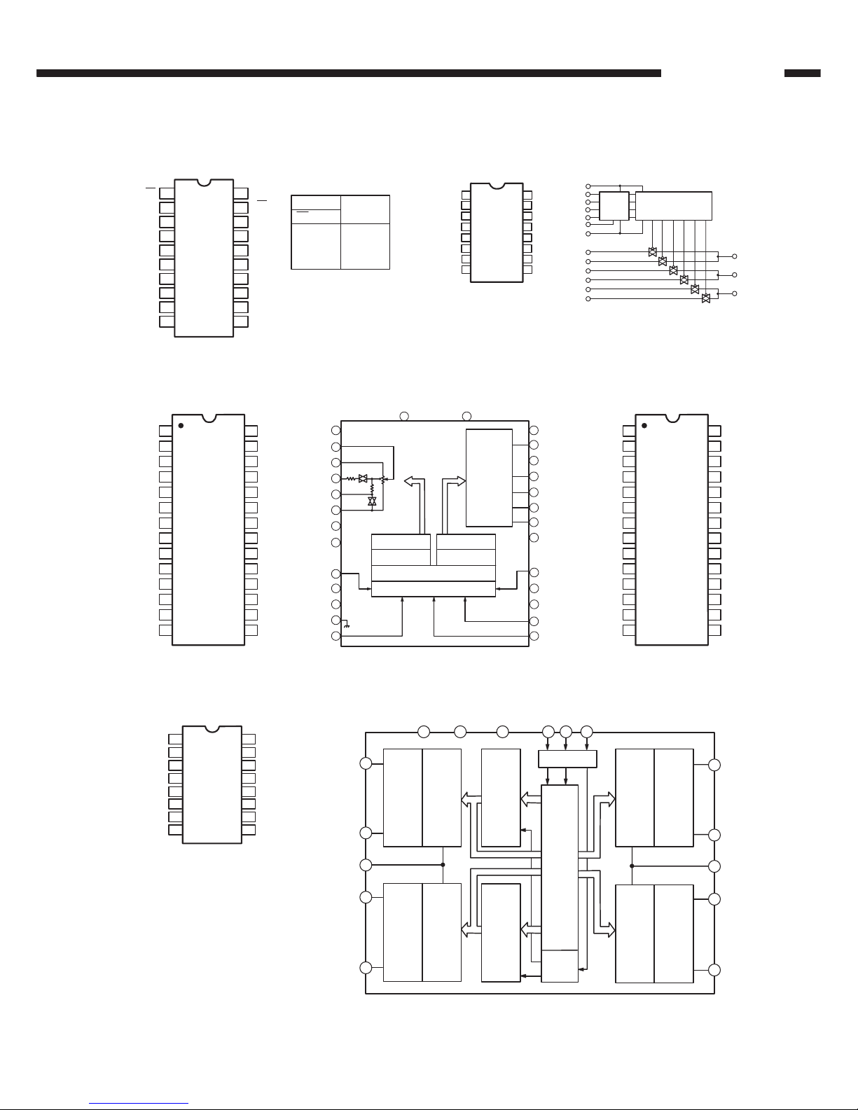
LC89055W (AU: IC800)
Pin Name
Function
LC89055W Terminal Function
Pin
No.
1 DISEL I Data input terminal (select input pin of DIN0, DIN1)
2 DOUT O Input bi-phase data through output terminal
3 DIN0 I Amp built-in coaxial/optical input correspond data input terminal
4 DIN1 I Amp built-in coaxial/optical input correspond data input terminal
5 DIN2 I Optical input correspond data input terminal
6 DGND Digital GND
7 DVDD Digital power supply
8 R I VCO gain control input terminal
9 VIN I VCO free-run frequency setting input terminal
10 LPF O PLL loop filter setting terminal
11 AVDD Analog power supply
12 AGND Analog GND
13 CKOUT O Clock output terminal (256fs, 384fs, 512fs, X′tal osc., VCO free-run osc.)
14 BCK O 64fs clock output terminal
15 LRCK O fs clock output terminal (L: Rch, H: Lch, I2S: Reverse)
16 DATAO O Data output terminal
17 XSTATE O Input data detecting result output terminal
18 DGND Digital GND
19 DVDD Digital power supply
20 XMCK O X′tal osc. clock output terminal (24.576MHz or 12.288MHz)
21 XOUT O X′tal osc. connection output terminal
22 XIN I X′tal osc. connection input terminal, external signal input possible (24.576MHz or 12.288MHz)
23 EMPHA O Emphasis information output terminal of channel status
24 AUDIO O Bit1 output terminal of channel status
25 CSFLAG O Top 40bit revise flag output terminal of channel status
26 F0/P0/C0 O Input fs cal. sig. out / data type out / input word inf. output terminal
27 F1/P1/C1 O Input fs cal. sig. out / data type out / input word inf. output terminal
28 F2/P2/C2 O Input fs cal. sig. out / data type out / input word inf. output terminal
29 VF/P3/C3 O Validity flag out / data type out / input word inf. output terminal
30 DVDD Digital power supply
31 DGND Digital GND
32 AUTO O Non PCM burst data transfer detect sig. output terminal
33 BPSYNC O Non PCM burst data preamble Pa, Pb, Pc, Pd sync sig. output terminal
34 ERROR O PLL lock error, data error flag output terminal
35 DO O CPU I/F read data output terminal
36 DI I CPU I/F write data input terminal
37 CE I CPU I/F chip enable input terminal
38 CL I CPU I/F clock input terminal
39 XSEL I Frequency select input pin of XIN X′tal osc. (24.576MHz or 12.288MHz)
40 MODE0 I Mode setting input terminal
41 MODE1 I Mode setting input terminal
42 DGND Digital GND
43 DVDD Digital power supply
44 DOSEL0 I Data output format select input terminal
45 DOSEL1 I Data output format select input terminal
46 CKSEL0 I Output clock select input terminal
47 CKSEL1 I Output clock select input terminal
48 XMODE I Reset input terminal
I/O
* For latch-up countermeasure, set digital (DVDD) and analog (AVDD) power on/off in the same timing.
D I S E L
D O U T
D I N 0
D I N 1
D I N 2
D G N D
D V D D
R
V I N
L P F
A V D D
A G N D
A U D I O
E M P H A
X I N
X O U T
X M C K
D V D D
D G N D
X S T A T E
D A T A 0
L R C K
B C K
C K O U T
C E
C L
X S E L
M O D E 0
M O D E 1
D G N D
D V D D
D O S E L 0
D O S E L 1
C K S E L 0
C K S E L 1
X M O D E
D I
D O
E R R O R
B P S Y N C
A U T O
D G N D
D V D D
V F / P 3 / C 3
F 2 / P 2 / C 2
F 1 / P 1 / C 1
F 0 / P 0 / C 0
C S F L A G
19
AVR-2802/982
M35015-210SP Terminal Function
Pin No. Symbol Name I/O Function
1 OSC1 Osc. circuit ext. I External terminal for indication oscillator circuit. Standard OSC. freq. is approx. 7MHz.
2 OSC2 terminal. O With this OSC. freq., decides horizontal indicatin and character width.
3 CS Chip select input I
Chip select terminal and turns to “L” when transfer serial data.
Hysteresis input. Pull up resistor is built-in.
4 SCK Serial clock input I
Takes in serial data of SIN at SCK rise when CS terminal is in “L”.
Hysteresis input. Pull up rersist is built-in.
5 SIN Serial data input I
Serial input of register for indication control and data, and address for indication data
memory. Hysteresis input. Pull up rersistor is built-in.
6 AC Auto-clear input I
Resets internal circuit of IC at “L” mode.
Hysteresi input. Pull up resistor is built-in.
7 V
DD2
Power supply
Power supply terminal of analog system. Connect to +5V.
8 CVIDEO
Combined
video output
O
Output terminal of combined video signal. Outputs 2Vp-p combined signal. Character
output, etc. Overlap CVIN signal and outputs at superimpose.
9 LECHA
Character level
input
I
Input terminal deciding character output level in combined video signal. color of character
is white.
10 CVIN
Combined video
input
I
Input terminal of external combined video signal.
Character output etc. overlap this external combined video signal.
11 Vss Ground
Ground terminal. Connect to GND.
12 P0 Output port p0 O
General output or character background signal BL NK1* output is switchable.
Polarity can be selected at ROM mask.
13 P1 Output port P1 O
General output or character background signal CO1* output is switchable.
Polarity can be selected at ROM mask.
14 P2 Output port P2 O
General output or character background signal BLNK2* output is switchable.
Polarity can be selected at ROM mask.
15 P3 Output port P3 O
General output or character background signal CO2* output is switchable.
Polarity can be selected at ROM mask.
16 OSCOUT O Terminal for external use of sync signal OSC. circuit. Use the freq.: 14.32MHz at NTSC
17 OSCIN I system, 17.73MHz at PAL. system, 14.30MHz at MPAL system.
18 HOR*
Horizontal sync
signal
I
Inputs horizontal sync signal.
Hysteresis input.
19 VERT*
Vertical sync
signal
Input vertical sync signal. Hysteresis input. Polarity can be selected at ROM mask.
20 V
DD1
Power supply I Power supply terminal of digital system. Connect to +5V.
Ext. terminal
for sync sig.
OSC. Circuit
M35015-210SP (AU: IC453)
1
2
3
4
5
6
7
8
9
1 0
1 1
1 2
1 3
1 4
1 5
1 6
1 7
1 8
1 9
2 0
O S C 1
O S C 2
C S
S C K
S I N
A C
V
D D 2
C V I D E O
L E C H A
C V I N
V
D D 1
V E R T *
H O R *
O S C I N
O S C O U T
P 3
P 2
P 1
P 0
V s s
C S
S C K
S I N
V
D D 1
2 0
A C
V s s
V
D D 2
P 1
P 0
C V I N
L E C H A
C V I D E O
O S C O U T
O S C I N
H O R *V E R T *O S C 2O S C 1
I N P U T
C O N T R O L
C IR C U I T
I N D I C A T IO N
O S C I L L A T O R
D A T A
C O N T R O L
C IR C U I T
A D D R E S S
C O N T R O L
C IR C U I T
T I M I N G
G E N E R A T O R
I N D I C A T IO N
C O N T R O L
R E G I S T E R
I N D I C A T IO N R A M
I N D I C A T IO N C H A R A C T E R R O M
B L IN K IN G C IR C U IT
S H I F T R E G I S T E R
I N D I C A T IO N
C O N T R O L C IR C U I T
R E A D O U T A D D R E S S
C O N T R O L C IR C U I T
I I N D I C A T IO N L O C A T I O N
D E T E C T I O N C I R C U IT
H C O U N T E R
S Y N C S I G N A L
S W I T C H I N G C I R C U IT
S Y N C S I G N A L D I S -
C R I M I N A T I N G C IR C U IT
O S C C I R C U I T
F O R S Y N C S I G N A L
G E N E R A T I O N
T I M I N G
G E N E R A T O R
N T S C
V I D E O O U T P U T
C IR C U I T
6
1 1
5
4
3
7
1 2 1 9 1 8
1 7
1 6
8
9
1 0
1 2
1 3
P 2
1 4
P 3
1 5
AVR-2802/982
20
AK4527BVQ (AU:IC602)
AK4527BVQ Terminal Function
1
2
3
4
5
6
7
8
9
10
11
12
13 14
15
16 17 18
192021
22
33
32
31
30
29
28
27
26
25
24
23
444342
41
40
39
38
37
36
35
34
SDOS
I2C
SMUTE
BICK
LRCK
SDTI1
DAUX
DFS
DZF2
RIN+
RIN–
ROUT1
L0OP1
L0OP0/SDA/CDTI
DIF1/SCL/CCLK
DIF0/CSL
P/S
MCLK
DZF1
AVSS
AVDD
VREFH
VCOM
DEM1
TVDD
PDN
ICKS2
CAD1
Top View
LIN+
LIN–
LOUT1
ROUT2
LOUT2
ROUT3
LOUT3
SDTI2
SDTI3
SDTO
DEM0
DVDD
DVSS
ICKS1
ICKS0
CAD0
Pin
No.
Pin Name I/O Function
1 SDOS I SDTO source select pin, L: Internal ADC output, H: DAUX input
2 I2C I Serial control mode select pin, L: 3-core serial, H: I2C bus
3 SMUTE I Soft mute pin, H: Soft mute start, L: Release
4 BICK I Audio serial data clock pin
5 LRCK I Input channel clock pin
6 SDTI1 I DAC1 audio serial data input pin
7 SDTI2 I DAC2 audio serial data input pin
8 SDTI3 I DAC3 audio serial data input pin
9 SDTO O Audio serial data output pin
10 DAUX I Auxiliary audio serial data input pin
11 DFS I Double speed sampling mode pin, L: Normal, H: Double
12 NC No Connect, No internal bonding
13 DZFE I Zero input detect enable pin
14 TVDD Power pin for output buffer, 2.7V~5.5V
15 DVDD Digital power pin, 4.5V~5.5V
16 DVss Digital GND pin, 0V
17 PDN I Power down & reset pin, L: Powered-down and register initialized, Reset with PDN when switching CAD0-1
18 TST I Test pin, connected to DVSS
19 NC No Connect, No internal bonding
20 ADIF I Analog Input Format Select pin
21 CAD1 I Chip address-1 pin
22 CAD0 I Chip address-0 pin
23 LOUT3 O DAC3L channel analog out pin
24 ROUT3 O DAC3R channel analog out pin
25 LOUT2 O DAC2L channel analog out pin
26 ROUT2 O DAC2R channel analog out pin
27 LOUT1 O DAC1L channel analog out pin
28 ROUT1 O DAC1R channel analog out pin
29 LIN- I L-ch analog inverted input pin
30 LIN+ I L-ch analog non-inverted input pin
31 RIN- I R-ch analog inverted input pin
32 RIN+ I R-ch analog non-inverted input pin
33 DZF2/OVF O 0 input detect 2 pin/Analog input overflow detect pin
34 VCOM O Common V-out pin, AVDD/2, connect large capacitor to avoid noise
35 VREFH I Ref. V input pin, AVDD
36 AVDD Analog GND pin, 4.5V~5.5V
37 AVss Analog GND pin, 0V
38 DZF1 O 0 input detect pin, H: Input data of G1 is 8192 times “0” in a raw or RSTN bit “0”, L: When P/S= “0”
39 MCLK I Master clock input pin
40 P/S I Parallel/Serial select pin, L: Serial control
DIF0 I Audio data I/F format 0 pin (parallel control)
41
CSN I Chip select pin (3-wire serial control), connect to DVDD when I2C bus control
DIFI I Audio data I/F format 1 pin (parallel control)
42
SCL/CCLK I Control data clock pin (serial control), I2C=”L”: CCLK (3-wire serial), I2C=”H”: SCL (I2C bus)
LOOP0 I Loop back mode 0 pin (parallel control), effects digital loop back ADC to all DAC
43
SDA/CDTI I/O Control data input pin (serial control), I
2
C=”L”: CCTI (3-wire serial), I2C=”H” SDA (I2C bus)
44 LOOP1 I Loop back mode 1 pin, from SDT1 to all DAC
21
AVR-2802/982
Symbol Function
CO: IC304
Q1 A Video input switching
Q2 B Video input switching
Q3 C Video input switching
Q4 D Video output switching
Q5 E Video output switching
Q6 F Video output switching
Q7 H Video output switching
Q8 G Video output switching
Port
Symbol Function
CO: IC305
Port
Q1
DIRECT/TONE DEFEAT
DIRECT & TONE DEFEAT relay control (H:DIRECT,TONE DEFEAT)
Q2 S1 Video signal switching control output
Q3 S2 Video signal switching control output
Q4 EXT. IN
Sub woofer channel gain control terminal (L:EXT. IN)
Q5 D Video output switching
Q6 G Video output switching
Q7 NC
Q8 FRONT A+B Current limiter control terminal (H:Front SP A+B)
BU4094BCF (CO: IC304,305)
BU2090F (CO: IC103)
1Vss
2DATA
3CLOCK
4LCK
5Q0
6Q1
7Q2
8Q3
9Q4
18
17
16
15
14
13
12
11
10
VDD
OE
Q11
Q10
Q9
Q8
Q7
Q6
Q5
CONTROL CIRCUIT
12-bit SHIFT RESISTER
12-bit STRAGE RESISTER
OUTPUT BUFFER (OPEN DRAIN)
STROBE
1
2
3
4
5
6
7
8
9
10
11
16
15
14
13
12
DATA
CLOCK
Q1
Q2
Q3
Q4
V
SS
VDD
OE
Q5
Q6
Q7
Q8
Q'
S
Q
S
LC75721E (CO: IC101)
64
49
48 33
32
17
161
AM 1
AM 2
AM 3
AM 4
AM 5
AM 6
AM 7
AM 8
AM 9
AM 10
AM 11
AM 12
AM 13
AM 14
AM 15
AM 16
AM 17
AM 18
AM 19
AM 20
AM 21
AM 22
AM 23
AM 24
AM 25
AM 26
AM 27
AM 28
AM 29
AM 30
AM 31
AM 32
G7 G8G9
G10
G11
AA8/G12
AA7/G13
AA6/G14
AA5/G15
AA4/G16
AA3
AA2
AA1
AM35
AM34
AM33
DI
CL
CE
RES
V
DD
OSCI
OSCO
Vss
TEST
V
FL
G1
G2
G3
G4
G5
G6
Symbol
V
DD
Vss
Power terminal +5V
Power terminal GND
V
FL
Power terminal FL drive
DI
CL
CE
Serial data transfer terminal
DI: Data
CL: Clock
CE: Chip enable
OSCI
OSCO
External CR connecting terminal
RES
System reset terminal
AM1~AM35
AA1~AA3
Anode output terminal
AA4/G16
AA5/G15
AA6/G14
AA7/G13
AA8/G12
Anode/Grid output terminal
G1~G11 Grid output terminal
TEST LSI test terminal
Function
LC75721E Terminal Function
1
2
3 45678 9 10 111213 14
15
16 171819
20
21
22
23
24
25
26
27
28
29
3031
32
33
34
35
36
37
3839
40
41
42
V
DD
V
SS
S1S2S3S4S5S6S7S8S9
S10
S11
S12
S13
S14
S15
S16
S17
S18
GND
CK
DATA
STB
S1S2S3S4S5S6S7S8S9
S10
S11
S12
S13
S14
S15
S16
S17
S18
18 bit Latch Circuit (Rch)
(Lch) Same as Rch
Level Shift + Shift Register Circuit
1
2
3 45678 9 10 11
12
13
14
15
16 171819
20
21
22
23
24
25
26
27
28
29
3031
32
33
34
35
36373839
40
41
42
V
DD
V
SS
S1S2S3S4S5S6S7S8S9
S10
S11
S12
S13
S14
S15
S16
S17
S18
GND
CK
DATA
STB
S1S2S3S4S5S6S7S8S9
S10
S11
S12
S13
S14
S15
S16
S17
S18
18 bit Latch Circuit (Rch)
(Lch) Same as Rch
Level Shift + Shift Register Circuit
TC9274N-011 (AU: IC107) TC9274N-017 (EX: IC312)
22
AVR-2802/982
TC9273N-004 (AU: IC108)
S2
S3
S4
S5
S6
S7
S8
S9
S10
S1
V
DD
STB
DATA
S2
S3
S4
S5
S6
S7
S8
S9
S10
GND
CK
Vss
S1
13
14
1
3
4
5
6
7
8
9
10
11
12
2
15
16
28
27
26
25
24
23
22
21
20
19
18
17
1
13
28
2~12
12~27
14
15
16
Vss
GND
V
DD
S1~S10
CK
DATA
STB
GND=0V
Vss=-8.0~-17V
GND=0V
Border Input
Pin No
Symbol Name
Function
Dual Power Use:VDD = 8.0~17 V Single Power Use:VDD = 8.0~18V
+Power Terminal
Digital Ground
+Power Terminal
I/O Terminal
Clock Input
Low level
Terminal
Clock input for data transfer.
Serial input for switch setting.
Strobe InputStrobe input for data writing.Strobe Input
Data Input
Input terminal of analog switch.
TC9273N Terminal Function
NJM2229S (AU: IC452)
3
2
4
6
7
8
9
10
11
12
13
14
1
15
16
5
1
16
Sync Sepa
Sync Det
Phase
Det
Vsync Sepa
32fH
VCO
1/32
AD1854 (AU: IC601)
1
2
3
4
5
6
7
8
9
10
11
12
13
14
28
27
26
25
24
23
22
21
20
19
18
17
16
15
DGND
MCLK
CLATCH
CCLK
CDATA
384/256
X2MCLK
ZEROR
DEEMP
96/48
AGND
OUTR+
OUTR−
FILTR
DVDD
SDATA
BCLK
L/RCLK
PD/RST
MUTE
ZEROL
IDPM0
IDPM1
FILTB
AVDD
OUTL+
OUTL−
AGND
FRONT VIEW
Name Function
Terminal Function
No.
1 DGND I Digital Ground.
2 MCLK I Master Clock Input
3 CLATCH I Latch input for control data
4 CCLK I Control clock input for control data
5 CDATA I Serial control input
6 384/256 I Selects the master clock mode
7 X2MCLK I Selects internal clock doubler (LO) or internal clock=MCLK (HI)
8 ZEROR O Right Channel Zero Flag Output
9 DEEMP I De-Emphasis
10 96/48 I Selects 48kHz (LO) or 96kHz Sample Frequency Control
11,15 AGND I Analog Ground
12 OUTR+ O Right Channel Positive line level analog output
13 OUTR- O Right Channel Negative line level analog output
14 FILTR O Voltage Reference Filter Capacitor Connection
16 OUTL- O Left Channel Negative line level analog output
17 OUTL+ O Left Channel Positive line level analog output
18 AVDD I Analog Power supply
19 FILTB O Filter Capacitor connection
20 IDPM1 I Input serial data port mode control one
21 IDPM0 I Input serial data port mode control zero
22 ZEROL O Left Channel Zero Flag output
23 MUTE I Mute. Assert HI to mute both stereo analog output
24 PD/RST I Power-Down/Reset
25 L/R CLK I Left/Right clock input for input data
26 BCLK I Bit clock input for input data
27 SDATA I Serial input
28 DVDD I Digital Power Supply
I/O
23
AVR-2802/982
SN74LV244APW (AU: IC818, 825)
1
2
3
4
5
6
7
8
10
9
20
19
18
17
16
15
14
13
12
11
1OE
1A1
2Y4
1A2
2Y3
1A3
2Y2
1A4
2Y1
GND
Vcc
2OE
1Y1
2A4
1Y2
2A3
1Y3
2A2
1Y4
2A1
INPUT
OUTPUT
OE A Y
L H H
L L L
H X Z
FUNCTION TABLE
(each buffer)
TOP VIEW
BU4053BCF (AU:IC256)
MM74HC4053SJ (AU: IC451)
C9
1
2
V
EE
3
4
5
6
7
8
9
1 0
11
1 6
1 5
1 4
1 3
12
Y1
Y0
Z-COM
Z0
INH
Vss
V
DD
Y-COM
X-COM
X1
X0
C
A
B
Z1
LEVEL
CONVER
-TER
BINARY TO 1 of 2
DECODER WITH INHIBIT
14 X
Z1 3
Z0 5
Y1 1
Y0 2
X1 13
X0 12
V
EE
7
B10
INH6
Vss8
A11
V
DD
16
15 Y
4 Z
TOP VIEW
L-LD2
9
L-ch7 to 91decoder
R-ch latch circuit
R-ch7 to 91decoder
10
19
NC
22
NC
3
2
4
5
6
7
8
11
12
13
14
28
27
26
25
24
23
21
20
18
17
16
15
1
NC
L-OUT
NC
L-IN
L-LD1
L-A-GND
NC
CS1
NC
GND
CK
V
SS
V
DD
NC
R-OUT
R-LD1
R-LD2
R-A-GND
NC
CS2
NC
STB
DATA
R-IN
50k
Ω
/
91S
TEP
VR
Same
as L-ch
L-ch latch circuit
Shift register (24Bit)
Level shift circuit
TC9459N
(EX: IC805)
1
2
3
4
5
6
7
8
9
10
11
12
13
14
28
27
26
25
24
23
22
21
20
19
18
17
16
15
Vss
NC
L-OUT
NC
L-IN
L-LD1
L-LD2
L-A-GND
NC
CS1
GND
CK
V
NC
R-OUT
NC
R-IN
R-LD1
R-LD2
R-A-GND
NC
CS2
DATA
NC
STB
NC
NC
DD
1
2
3
4
5
6
7
8
9
10
11
12
13
14
28
27
26
25
24
23
22
21
20
19
18
17
16
15
Vss
NC
L-OUTA
L-A-GNDB
CS1
GND
CK
V
TEST
R-OUTA
R-A-GNDB
DATA
L-A-GNDC
STB
DD
L-INC
L-OUTC
L-INB
L-OUTB
L-A-GNDA
L-INA
CS2
R-A-GNDC
R-INC
R-OUTC
R-INB
R-OUTB
R-A-GNDA
R-INA
TC9482N
(EX: IC809)
TOP VIEW TOP VIEW
TC9184AP (EX: IC102)
2
3
4
5
6
1
16
7
8
9
10
15
14
13
12
11
BASS+
BASS-
COM
TREBLE-
TREBLE+
VSS
VDD
GND
CK
DATA
STB
BASS+
BASS-
COM
TREBLE-
TREBLE+
Ladder resister
Analog switch
13 bit latch circuit
Level shift
20 bit Shift register circuit
Analog switch
Ladder resister
Ladder resister
Analog switch
13 bit latch circuit
Code
detect
circuit
Analog switch
Ladder resister
BASS+
BASS-
COM
TREBLE+
TREBLE-
GND
CK
1
2
3
4
5
6
7
8
16
15
14
13
12
11
10
9
V
STB
DATA
Vss
5
DD
TREBLE+
TREBLE-
COM
BASS+
BASS-
TOP VIEW
NC
NC
 Loading...