

Page 1
Page 2

DVP-ES2/EX2/SS2/SA2/SX2/SE
Operation Manual
Programming
Publication History
Issue Description of Changes Date
First
Edition
Second
Edition
The first edition is issued. 2010/08/04
1. Chapter 2.8 M Relay: Add M1037, M1119, M1182,
M1308, M1346, and M1356, and update the
description of the functions of M1055~M1057and
M1183.
2. Chapter 2.13 Special Data Register: Add D1037,
D1312, D1354, and D1900~D1931, and modify the
attributes of the latched functions of D1062,
D1114, D1115, and D1118.
3. Chapter 2.16 Applications of Special M Relays and
D Registers: Update the description of the
functions of RTCs; add M1037, D1037( Enable SPD
function), M1119( Enable 2-speed ou tput function
of DDRVI instruction) , M1308, D1312( Output
specified pulses or seek Z phase signal when zero
point is achieved) , and M1346( Output clear
signals when ZRN is completed); Easy PLC Link is
changed to PLC Link, and the description is added.
4. Chapter 3.1 Basic Instructions (without API
numbers) and Chapter 3.2 Explanations to Basic
Instructions: Add NP and PN instructions, and add
Chapter 3.7 Numerical List of Instructions (in
alphabetic order)
5. Chapter 3.6 Numerical List of Instructions and
Chapter 3.8 Detailed Instruction Explanation:
Increase explanations of DSPA instruction, and
add floating-point contact type comparison
instructions FLD=, FLD>, FLD<, FLD<>, FLD<=,
FLD>=, FAND=, FAND>, FAND<, FAND<>,
FAND<=, FAND>=, FOR=, FOR>, FOR<, FOR<>,
FOR<=, FOR>=; add the supplementary
description of PLSR instruction and the description
of K11~K19 in DTM instruction mode; update the
description of API166 instruction.
2011/09/15
Page 3

Issue Description of Changes Date
1. SE is added in the title of the manual.
2. Chapter 2.16: The default value in D1062 is K10.
3. API 15 in Chapter 3: The contents about S<D are
deleted in program example 3.
Third
Edition
4. API 148 and API 149 are added in chapter 3.
5. The information related to DVP-SE is added.
6. The information related to DVP32ES-C is added.
7. The descriptions of the models are added in the
contents.
8. Appendix A is added.
2012/05/31
Page 4

DVP-ES2/EX2/SS2/SA2/SX2/SE
Operation Manual
Programming
Contents
1 PLC Concepts
1.1 PLC Scan Method……………………………………………………………………………... 1-2
1.2 Current Flow……………………………………………………………………………………. 1-3
1.3 NO Contact, NC Contact……………………………………………………………………… 1-3
1.4 PLC Registers and Relays………………………………………………………… …………. 1-4
1.5 Ladder Logic Symbols…………………………………………………… …………………… 1-5
1.5.1 Creating a PLC Ladder Program…………………………………………………... 1-6
1.5.2 LD / LDI (Load NO contact / Load NC contact)…………………………………... 1-7
1.5.3 LDP / LDF (Load Rising edge trigger/ Load Falling edge trigger)……………… 1-7
1.5.4 AND / ANI (Connect NO contact in series / Connect NC contact in series)…... 1-7
1.5.5 ANDP / ANDF (Connect Rising edge in series/ Connect Falling edge in
series)…………………………………………………………………………………. 1-7
1.5.6 OR / ORI (Connect NO contact in parallel / Connect NC contact in parallel)…. 1-8
1.5.7 ORP / ORF (Connect Rising edge in parallel/ Connect Falling edge in
parallel)……………………………………………………………………………….. 1-8
1.5.8 ANB (Connect block in series)……………………………………………………... 1-8
1.5.9 ORB (Connect block in parallel)……………………………………………………. 1-8
1.5.10 MPS / MRD / MPP (Branch instructions)………………………………………….. 1-8
1.5.11 STL (Step Ladder Programming)…………………………………………………... 1-9
1.5.12 RET (Return)…………………………………………………………………………. 1-10
1.6 Conversion between Ladder Diagram and Instruction List Mode…………… …………… 1-11
1.7 Fuzzy Syntax…………………………………………………………………………………… 1-12
1.8 Correcting Ladder Diagram…………………………………………………………………… 1-14
1.9 Basic Program Design Examples……………………………………………………………. 1-16
2 Programming Concepts
2.1 ES2/EX2 Memory Map……………………………………………………………………….. 2-2
2.2 SS2 Memory Map…………………………………………………………………………….. 2-5
2.3 SA2 Memory Map…………………………………………………………………………….. 2-8
2.4 SX2 Memory Map…………………………………………………………………………….. 2-11
2.5 Status and Allocation of Latched Memory………………………………………………….. 2-14
2.6 PLC Bits, Nibbles, Bytes, Words, etc……………………………………………………….. 2-15
2.7 Binary, Octal, Decimal, BCD, Hex…………………………………………………………… 2-15
2.8 M Relay………………………………………………………………………………………… 2-17
2.9 S Relay………………………………………………………………………………………… 2-30
2.10 T (Timer) …………… ………………………………………………………………………… 2-30
2.11 C (Counter) …………………………………………………………………………………… 2-31
2.12 High-speed Counters………………………………………………………………………… 2-34
2.13 Special Data Register………………………………………………………………………… 2-39
2.14 E, F Index Registers…………………………………………………………………..……… 2-51
2.15 Nest Level Pointer[N], Pointer[P], Interrupt Pointer [I] …………………..……………….. 2-51
2.16 Applications of Special M Relays and D Registers……………………...………………… 2-55
3 Instruction Set
3.1 Basic Instructions (without API numbers) ………………………..………………………… 3-2
i
Page 5

3.2 Explanations to Basic Instructions…………………………………………………………... 3-3
3.3 Pointers………………………………………………………………………………………… 3-12
3.4 Interrupt Pointers……………………………………………………………………………… 3-12
3.5 Application Programming Instructions……………………………………………………… 3-14
3.6 Numerical List of Instructions (classified according to the function)…………………….. 3-24
3.7 Numerical List of Instructions (in alphabetic order)……………………………………….. 3-33
3.8 Detailed Instruction Explanation…………………………………………………………….. 3-42
4 Communications
4.1 Communication Ports…………………………………………………………………………. 4-2
4.2 Communication Protocol ASCII mode……………………………………………………….. 4-3
4.2.1 ADR (Communication Address) …………………………………………………… 4-3
4.2.2 CMD (Command code) and DATA………………………………………………… 4-3
4.2.3 LRC CHK (checksum) ……………………………………………………………… 4-5
4.3 Communication Protocol RTU mode………………………………………………………… 4-7
4.3.1 Address (Communication Address) ………………………………………………. 4-7
4.3.2 CMD (Command code) and DATA………………………………………………… 4-8
4.3.3 CRC CHK (check sum) …………………………………………………………….. 4-9
4.4 PLC Device Address…………………………………………………………………………... 4-11
4.5 Command Code……………………………………………………………………………….. 4-13
4.5.1 Command Code: 01, Read Status of Contact (Input point X is not included)… 4-13
4.5.2 Command Code: 02, Read Status of Contact (Input point X is included)……... 4-14
4.5.3 Command Code: 03, Read Content of Register (T, C, D)………………………. 4-15
4.5.4 Command Code: 05, Force ON/OFF single contact………………………… ….. 4-16
4.5.5 Command Code: 06, Set content of single register……………………………… 4-17
4.5.6 Command Code: 15, Force ON/OFF multiple contacts…………………………. 4-18
4.5.7 Command Code: 16, Set content of multiple registers………………………….. 4-18
5 Sequential Function Chart
5.1 Step Ladder Instruction [STL], [RET] ………………………………………………………. 5-2
5.2 Sequential Function Chart (SFC) …………………………………………………………… 5-2
5.3 The Operation of STL Program……………………………………………………………… 5-4
5.4 Points to Note for Designing a Step Ladder Program…………………………………….. 5-9
5.5 Types of Sequences………………………………………………………………………….. 5-11
5.6 IST Instruction…………………………………………………………………………………. 5-22
6 Troubleshooting
6.1 Common Problems and Solutions…………………………………………………………... 6-2
6.2 Error code Table (Hex) …………………………………………………………................... 6-4
6.3 Error Detection Devices………………………………………………………….................. 6-6
7 CANopen Function and Operation
7.1 The Introduction of CANopen…………………………………………………………........... 7-2
7.1.1 The Description of the CANopen Functions……………………………………… 7-2
7.1.2 The Input/Output Mapping Areas………………………………………………….. 7-3
7.2 The Installation and the Network Topology…………………………………………………. 7-3
7.2.1 The Dimensions…………………………………………………………................. 7-3
7.2.2 The Profile………………………………………………………….......................... 7-4
7.2.3 The CAN Interface and the Network Topology…………………………………… 7-4
7.3 The CANopen Protocol………………………………………………………….................... 7-8
7.3.1 The Introduction of the CANopen Protocol……………………………………….. 7-8
7.3.2 The CANopen Communication Object………………………… …………………. 7-9
7.3.3 The Predefined Connection Set…………………………………………………… 7-14
ii
Page 6

7.4 Sending SDO, NMT and Reading Emergency Message through the Ladder Diagram... 7-15
7.4.1 Data St ructure of SDO Request Message………………………………………... 7-15
7.4.2 Data Structure of NMT Message…………………………………………………... 7-18
7.4.3 Data Structure of EMERGENCY Request Message…………………………….. 7-19
7.4.4 Example on Sending SDO through the Ladder Diagram……………………….. 7-21
7.5 Indicators and Troubleshooting…………………………………………………………........ 7-23
7.5.1 Description of Indicators…………………………………………………………..... 7-23
7.5.2 CANopen Network Node S tate Display…………………………………………… 7-24
7.6 Application Example…………………………………………………………......................... 7-27
7.7 Object Dictionary………………………………………………………….............................. 7-35
Appendix A
A.1 Installing the USB Driver…………………………………………… ……………................. A-2
iii
Page 7

The DVP-ES2 series PLCs, the DVP-ES2-C series PLCs, the DVP-EX2 series
PLCs, the DVP-SS2 series PLCs, the DVP-SA2 series PLCs, the DVP-SX2
series PLCs, and the DVP-SE series PLCs are listed below.
Series Model name
DVP16ES200R, DVP16ES200T, DVP24ES200R, DVP24ES200T,
DVP-ES2
DVP32ES200R, DVP32ES200T, DVP32ES211T, DVP40ES200R,
DVP40ES200T, DVP60ES200R, DVP60ES200T,
DVP32ES200RC, DVP32ES200TC
DVP-ES2-C
DVP-EX2
DVP-SS2
DVP-SA2
DVP-SX2
DVP-SE
DVP32ES200RC, DVP32ES200TC
DVP20EX200R, DVP20EX200T, DVP30EX200R, DVP30EX200T
DVP14SS211R, DVP14SS211T
DVP12SA211R, DVP12SA211T
DVP20SX211R, DVP20SX211S, DVP20SX211T
DVP12SE11R, DVP12SE11T
iv
Page 8

v
Page 9

PLC Concepts
This chapter introduces basic and advanced concepts of ladder logic, which is the mostly
adopted programming language of PLC. Users familiar with the PLC concepts can move to
the next chapter for further programming concepts. However, for users not familiar with the
operating principles of PLC, please refer to this chapter to get a full understanding of PLC
concepts.
Chapter Contents
PLC Scan Method...............................................................................................................1-2
1.1
1.2 Current Flow........................................................................................................................1-3
1.3 NO Contact, NC Contact ....................................................................................................1-3
1.4 PLC Registers and Relays.................................................................................................1-4
1.5 Ladder Logic Symbols.......................................................................................................1-5
1.5.1 Creating a PLC Ladder Program...........................................................................1-6
1.5.2 LD / LDI (Load NO contact / Load NC contact).....................................................1-7
1.5.3 LDP / LDF (Load Rising edge trigger/ Load Falling edge trigger).........................1-7
1.5.4 AND / ANI (Connect NO contact in series / Connect NC contact in series)..........1-7
1.5.5 ANDP / ANDF (Connect Rising edge in series/ Connect Falling edge in series)..1-7
1.5.6 OR / ORI (Connect NO contact in parallel / Connect NC contact in parallel) .......1-8
1.5.7 ORP / ORF (Connect Rising edge in parallel/ Connect Falling edge in parallel)..1-8
1.5.8 ANB (Connect block in series) ..............................................................................1-8
1.5.9 ORB (Connect block in parallel)............................................................................1-8
1.5.10 MPS / MRD / MPP (Branch instructions) ..............................................................1-8
1.5.11 STL (Step Ladder Programming) ..........................................................................1-9
1.5.12 RET (Return) .......................................................................................................1-10
1.6 Conversion between Ladder Diagram and Instruction List Mode...............................1-1 1
1.7 Fuzzy Syntax.....................................................................................................................1-12
1.8 Correcting Ladder Diagram.............................................................................................1-14
1.9 Basic Program Design Examples ...................................................................................1-16
1-1
Page 10
DVP-ES2/EX2/SS2/SA2/SX2/SE Operation Manual - Programming
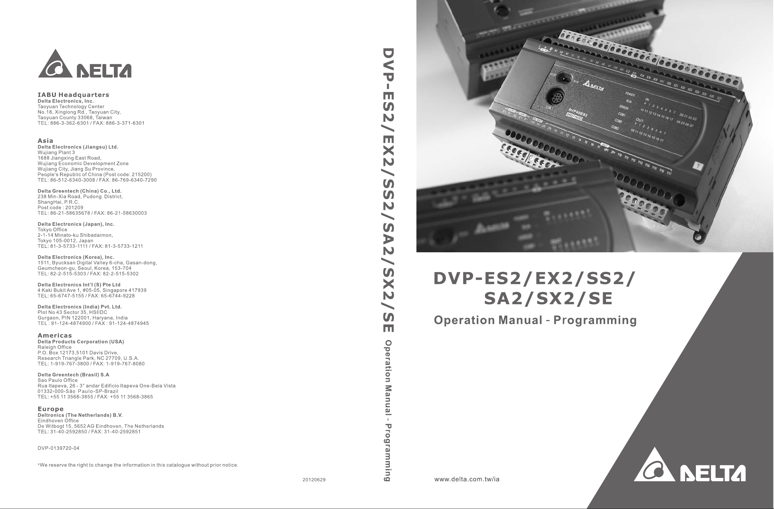
1.1 PLC Scan Method
PLC utilizes a standard scan method when evaluating user program.
Scanning process:
Scan input status
Evaluate user program
Refresh the outputs
Input sig nal
Program
Output
Input X
Input terminal
Store to memory
Input signal memory
Read X0 status from memory
X0
Y0
Read Y0 state from memory
Y0
M0
Output latched memory
Read the physical input status and store the data in internal
memory.
Evaluate the user program with data stored in internal memory.
Program scanning starts from up to down and left to right until
reaching the end of the program.
Write the evaluated data to the physical outputs
Input signal:
PLC reads the ON/OFF status of each input and
stores the status into memory before evaluating
the user program.
Once the external input status is stored into
internal memory, any change at the external
inputs will not be updated until next scan cycle
Writ e Y0 stat e into
Device Memory
starts.
Program:
PLC executes instructions in user program from
top to down and left to right then stores the
Write M0 state into
Output
evaluated data into internal memory. Some of this
memory is latched.
Output:
When END command is reached the program
Output terminal
evaluation is complete. The output memory is
transferred to the external physical outputs.
Output Y
Scan time
The duration of the full scan cycle (read, evaluate, write) is called “scan time.” With more I/O or
longer program, scan time becomes longer.
PLC measures its own scan time and stores the value (0.1ms) in register
Read
scan time
Measure
scan time
D1010, minimum scan time in register D1011, and maximum scan time in
register D1012.
Scan time can also be measured by toggling an output every scan and then
measuring the pulse width on the output being toggled.
Scan time can be calculated by adding the known time required for each
Calculate
scan time
instruction in the user program. For scan time information of individual
instruction please refer to Ch3 in this manual.
1-2
Page 11
1. PLC Concepts
Scan time exception
PLC can process certain items faster than the scan time. Some of these items interrupts and halt
the scan time to process the interrupt subroutine program. A direct I/O refresh instruction REF
allows the PLC to access I/O immediately during user program evaluation instead of waiting until
the next scan cycle.
1.2 Current Flow
Ladder logic follows a left to right principle. In the example below, the current flows through paths
started from either X0 or X3.
X0
X1 X2
Y0
Y0
X3
Reverse Current
When a current flows from right to left, which makes a reverse current logic, an error will be
detected when compiling the program. The example below shows the reverse current flow.
X0
X4
X1
X2
Y0
Y0
X3
a
X4 X5
b
X6
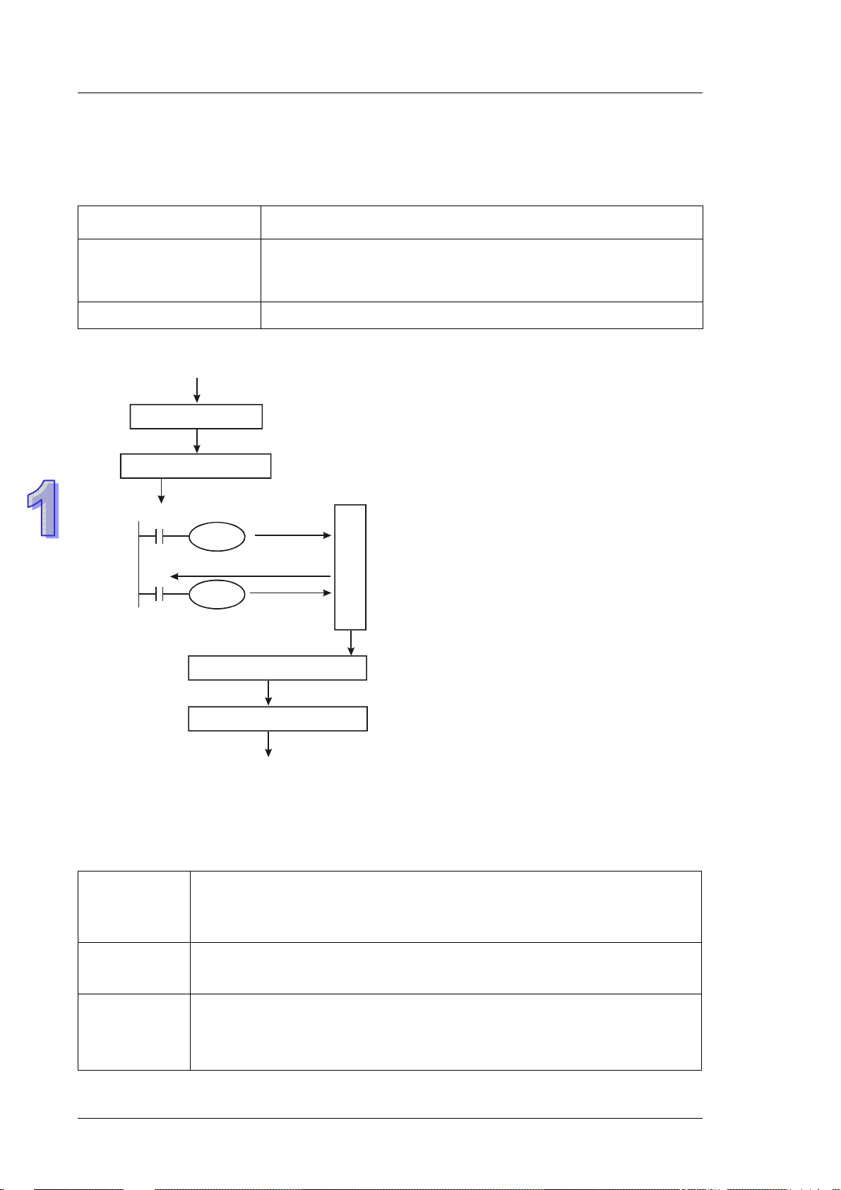
1.3 NO Contact, NC Contact
NO contact
Normally Open Contact, A contact
NC Contact
Normally Closed Contact, B contact
1-3
Page 12

DVP-ES2/EX2/SS2/SA2/SX2/SE Operation Manual - Programming
1.4 PLC Registers and Relays
Introduction to the basic internal devices in a PLC
Bit memory represents the physical input points and receives external input
X
(Input Relay)
Y
(Output Relay)
M
(Internal Relay)
S
(Step Relay)
signals.
Device indication: Indicated as X and numbered in octal, e.g. X0~X7,
X10~X17…X377
Bit memory represents the physical output points and saves the status to be
refreshed to physical output devices.
Device indication: Indicated as Y and numbered in octal, e.g. Y0~Y7,
Y10~Y17. ..Y377
Bit memory indicates PLC status.
Device indication: Indicated as M and numbered in decimal, e.g. M0, M1,
M2…M4095
Bit memory indicates PLC status in Step Function Control (SFC) mode. If no
STL instruction is applied in program, step point S can be used as an internal
relay M as well as an annunciator.
Device indication: Indicated as S and numbered in decimal, e.g. S0, S1,
S2…S1023
T
(Relay)
(Word)
(Dword)
C
(Counter)
(Relay)
(Word)
(Dword)
D
(Data register)
(Word)
E, F
(Index register)
(Word)
Bit, word or double word memory used for timing
register in it. When its coil is ON and the set time is reached, the associated
contact will be energized. Every timer has its resolution (unit:
1ms/10ms/100ms).
and has coil, contact and
Device indication: Indicated as T and numbered in decimal, e.g. T0, T1,
T2…T255
Bit, word or double word memory used for counting and has coil, contact and
register in it. The counter count once (1 pulse) when the coil goes from OFF to
ON. When the predefined counter value is reached, the associated contact will
be energized. There are 16-bit and 32-bit high-speed counters available for
users.
Device indication: Indicated as C and numbered in decimal, e.g. C0, C1,
C2…C255
Word memory stores values and parameters for data operations. Every
register is able to store a word (16-bit binary value). A double word will occupy
2 consecutive data registers.
Device indication: Indicated as D and numbered in decimal, e.g. D0, D1,
D2…D4999
Word memory used as a modifier to indicate a specified device (word and
double word) by defining an offset. Index registers not used as a m odifier can
be used as general purpose register.
Device indication: indicated as E0 ~ E7 and F0 ~ F7.
1-4
Page 13
1. PLC Concepts
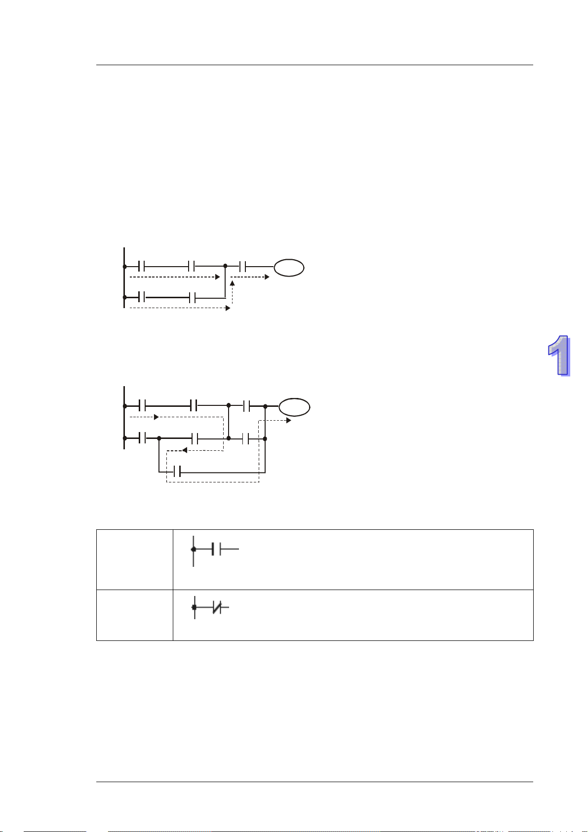
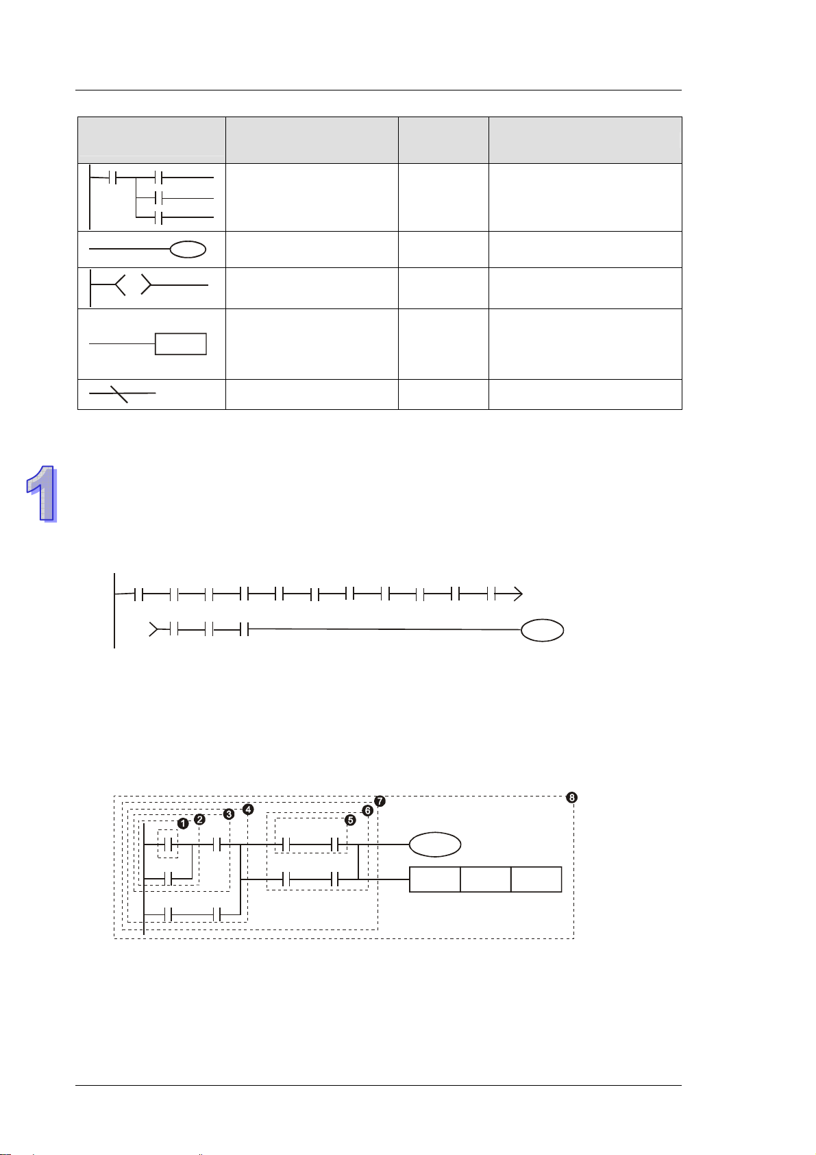
1.5 Ladder Logic Symbols
The following table displays list of WPLSoft symbols their descripti on, command, and memory
registers that are able to use the symbol.
Ladder Diagram
Structure
Explanation Instruction Available Devices
NO (Normally Open)
contact / A contact
NC (Normally Closed)
contact / B contact
NO contact in series
NC contact in series
NO contact in parallel
NC contact in parallel
Rising-edge trigger
switch
LD X, Y, M, S, T, C
LDI X, Y, M, S, T, C
AND X, Y, M, S, T, C
ANI X, Y, M, S, T, C
OR X, Y, M, S, T, C
ORI X, Y, M, S, T, C
LDP X, Y, M, S, T, C
Falling-edge trigger
switch
Rising-edge trigger in
series
Falling-edge trigger in
series
Rising-edge trigger in
parallel
Falling-edge trigger in
parallel
Block in series
LDF X, Y, M, S, T, C
ANDP X, Y, M, S, T, C
ANDF X, Y, M, S, T, C
ORP X, Y, M, S, T, C
ORF X, Y, M, S, T, C
ANB None
Block in parallel
ORB None
1-5
Page 14
DVP-ES2/EX2/SS2/SA2/SX2/SE Operation Manual - Programming
Ladder Diagram
Structure
Explanation Instruction Available Devices
MPS
S
Multiple output branches
Output coil
Step ladder
MRD
None
MPP
OUT Y, M, S
STL S
Basic / Application
instruction
Inverse logic
-
INV None
Basic instructions and API
instructions. Please refer to
chapter 3 Instruction Set
1.5.1 Creating a PLC Ladder Program
The editing of the program should start from the left side bus line to the right side bus line, and from
up to down. However, the right side bus line is omitted when editing in WPLSoft. A single row can
have maximum 11 contacts on it. If more than 11 contacts are connected, a continuous symbol “0”
will be generated automatically and the 12th contact will be placed at the start of next row. The
same input points can be used repeatedly. See the figure below:
X1 X2
X0
X12 X13
X11
0
X4 X5 X6 X7
X3
X10
C0
C1
0
Y1
When evaluating the user program, PLC scan starts from left to right and proceeds to next row
down until the PLC reaches END instruction. Output coils and basic / application instructions
belong to the output process and are placed at the right of ladder diagram. The sample program
below explains the execution order of a ladder diagram. The numbers in the black circles indicate
the execution order.
1-6
X0 X1 Y1 X4
Y1
M0
X3
M1
T0
M3
TMR T0 K10
Page 15
Execution order of the sample program:
1 LD X0
2 OR M0
3 AND X1
4 LD X3
AND M1
ORB
5 LD Y1
AND X4
6 LD T0
AND M3
ORB
7 ANB
8 OUT Y1
TMR T0 K10
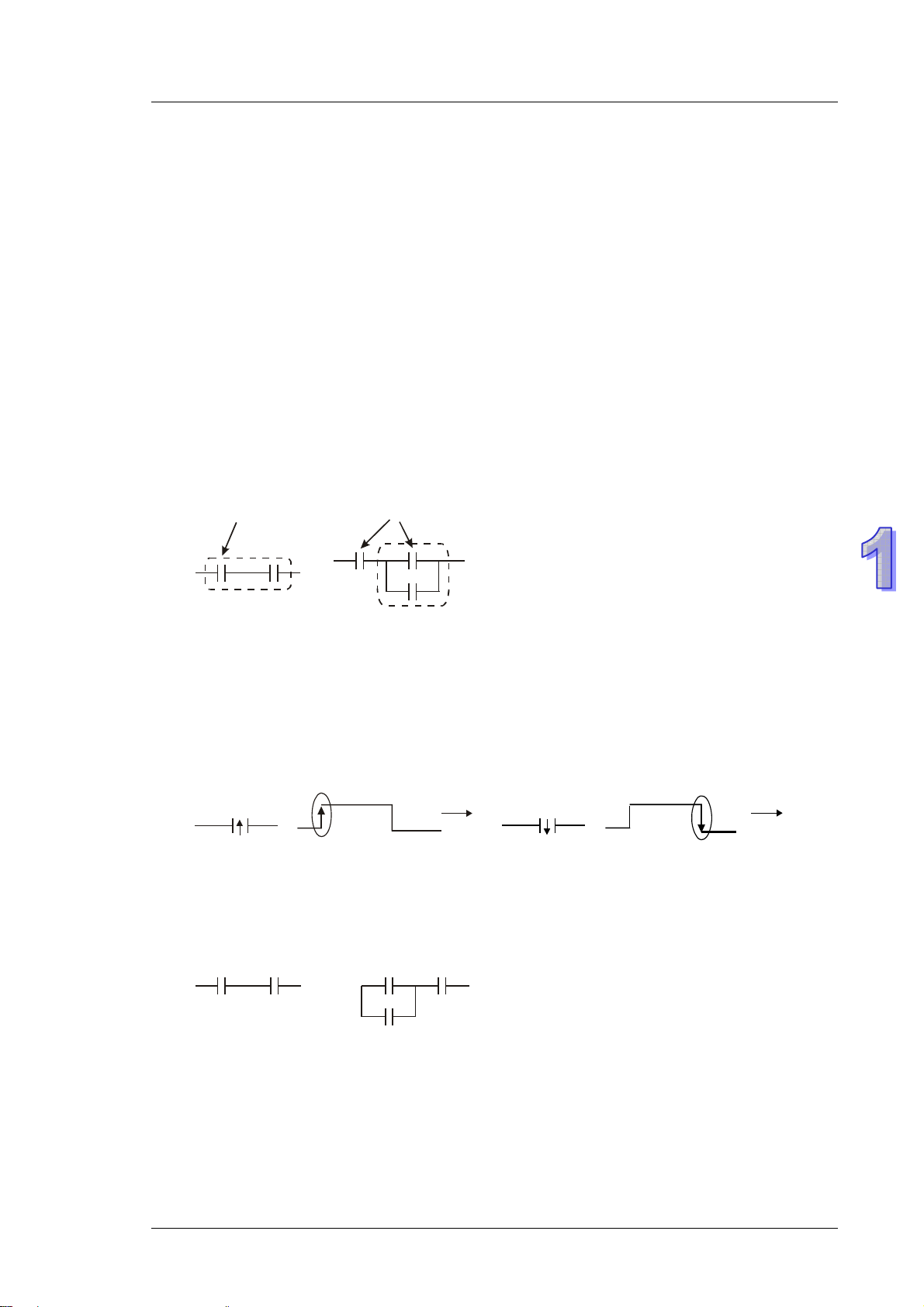
1.5.2 LD / LDI (Load NO contact / Load NC contact)
LD or LDI starts a row or block
LD instruction LD instruction
1. PLC Concepts
AND block OR bl oc k
1.5.3 LDP / LDF (Load Rising edge trigger/ Load Falling edge trigger)
Similar to LD instruction, LDP and LDF instructions only act at the rising edge or falling edge when
the contact is ON, as shown in the figure below.
X0
Rising-edge
OFF
ON
OFF
Time
X0
OFF
Falling-edge
ON
OFF
Time
1.5.4 AND / ANI (Connect NO contact in series / Connect NC contact in series)
AND (ANI) instruction connects a NO (NC) contact in series with another device or block.
AND instruction AND instruction
1.5.5 ANDP / ANDF (Connect Rising edge in series/ Connect Falling edge in series)
Similar to AND instruction, ANDP (ANDF) instruction connects rising (falling) edge triggers in series
with another device or block.
1-7
Page 16
DVP-ES2/EX2/SS2/SA2/SX2/SE Operation Manual - Programming
1.5.6 OR / ORI (Connect NO contact in parallel / Connect NC contact in parallel)
OR (ORI) instruction connects a NO (NC) in parallel with another device or block.
OR instruction OR instruction OR instruction
1.5.7 ORP / ORF (Connect Rising edge in parallel/ Connect Falling edge in parallel)
Similar to OR instruction, ORP (ORF) instruction connects rising (falling) edge triggers in parallel
with another device or block
1.5.8 ANB (Connect block in series)
ANB instruction connects a block in series with another block
ANB command
1.5.9 ORB (Connect block in parallel)
ORB instruction connects a block in parallel with another block
ORB instruction
1.5.10 MPS / MRD / MPP (Branch instructions)
These instructions provide a method to create multiplexed output branches based on current result
stored by MPS instruction.
1-8
Page 17
1. PLC Concepts
Branch
instruction
Branch
Symbol
Description
Start of branches. Stores current result of
MPS
┬
program evaluation. Max. 8 MPS-MPP pairs can
be applied
MRD
MPP
├
└
Reads the stored current result from previous
MPS
End of branches. Pops (reads then resets) the
stored result in previous MPS
Note: When compiling ladder diagram with WPLSoft, MPS, MRD and MPP could be automatically
added to the compiled results in instruction format. However, sometimes the branch instructions
are ignored by WPLSoft if not necessary. Users programming in instruction format can enter branch
instructions as required.
Connection points of MPS, MRD and MPP:
MPS
MPS
MRD
MPP
MPP
Note: Ladder diagram editor in ISPSoft does not support MPS, MRD and MPP instructions. To
achieve the same results as branch instructions, users have to connect all branches to the left
hand bus bar.
WPLSoft
ISPSoft
1.5.11 STL (Step Ladder Programming)
STL programming uses step points, e.g. S0 S21, S22, which allow users to program in a clearer
and understandable way as drawing a flow chart. The program will proceed to next step only if the
previous step is completed, therefore it forms a sequential control process similar to SFC
(Sequential Function Chart) mode. The STL sequence can be converted into a PLC ladder diagram
which is called “step ladder diagram” as below.
1-9
Page 18
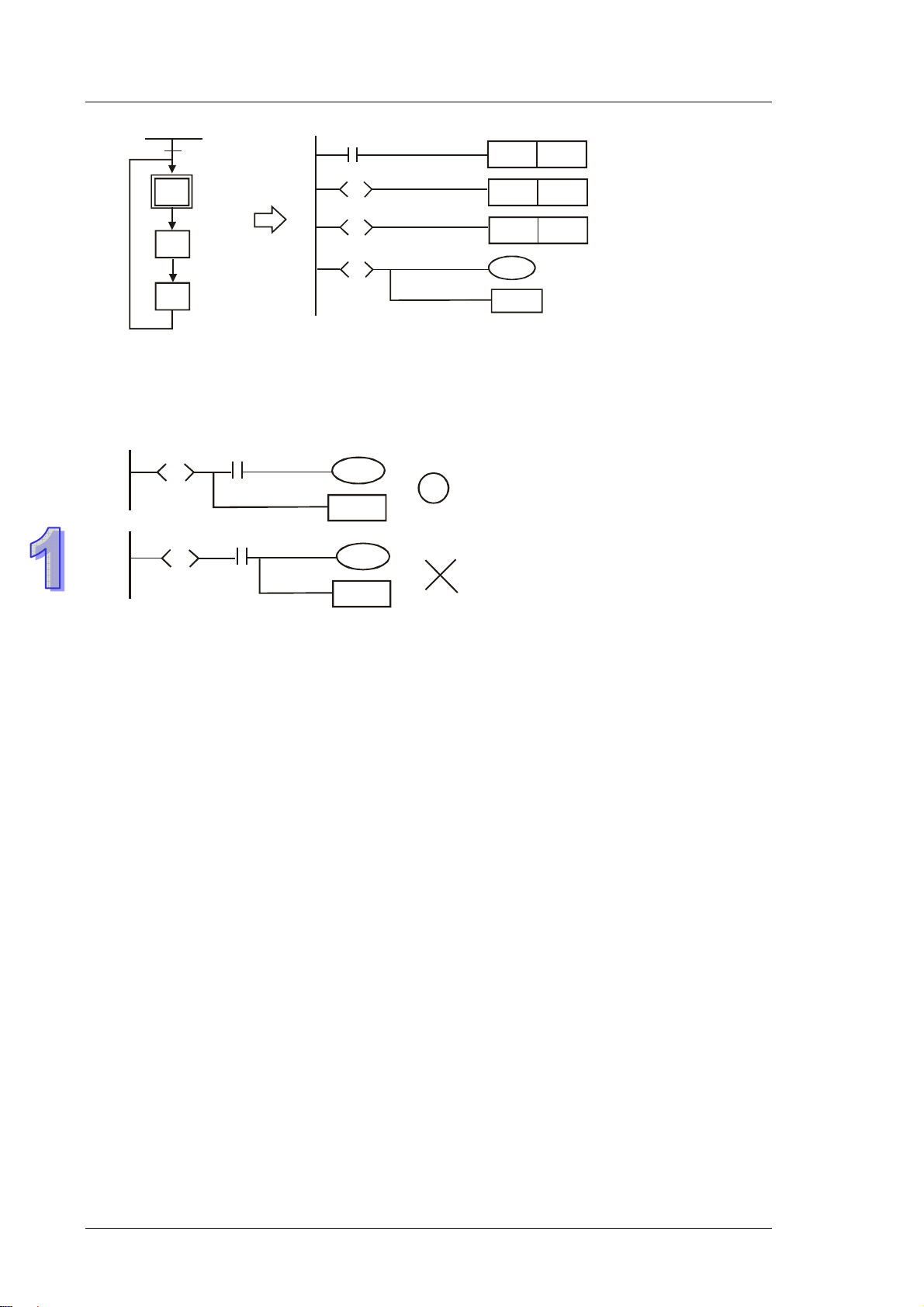
DVP-ES2/EX2/SS2/SA2/SX2/SE Operation Manual - Programming
M1002
S0
S21
M1002
initial
pulse
S0
S
S21
S
S22
S
SET
SET
SET
e
S0
S0
S21
S22
S22
RET
1.5.12 RET (Return)
RET instruction has to be placed at the end of sequential control process to indicate the com pletion
of STL flow.
S20
e
S
RET
S20
e
S
RET
Note: Always connect RET instruction immediately after the last step point indicated as the above
diagram otherwise program error may occur.
1-10
Page 19
1. PLC Concepts
Y
Y
Y
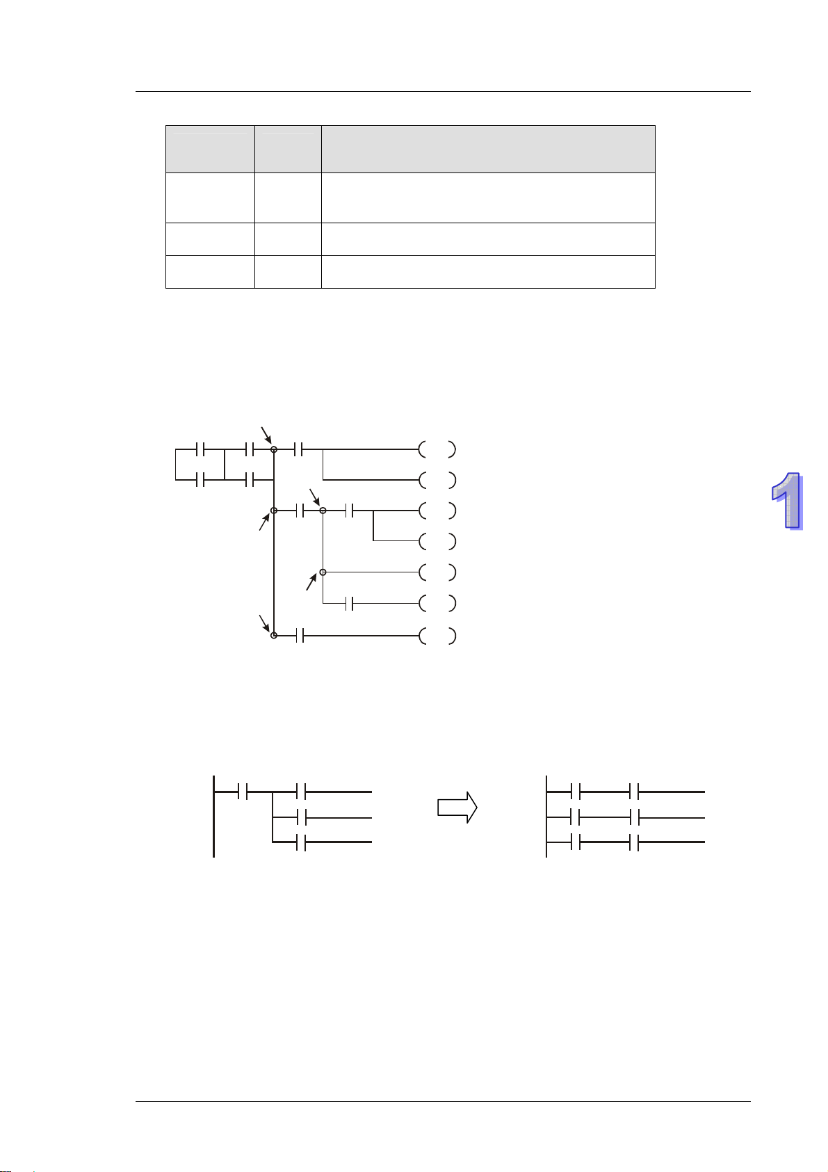
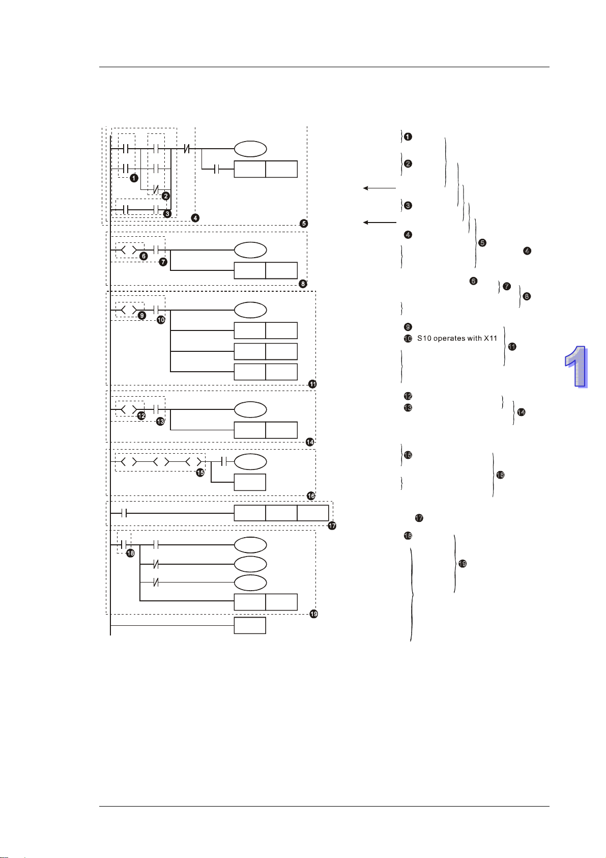
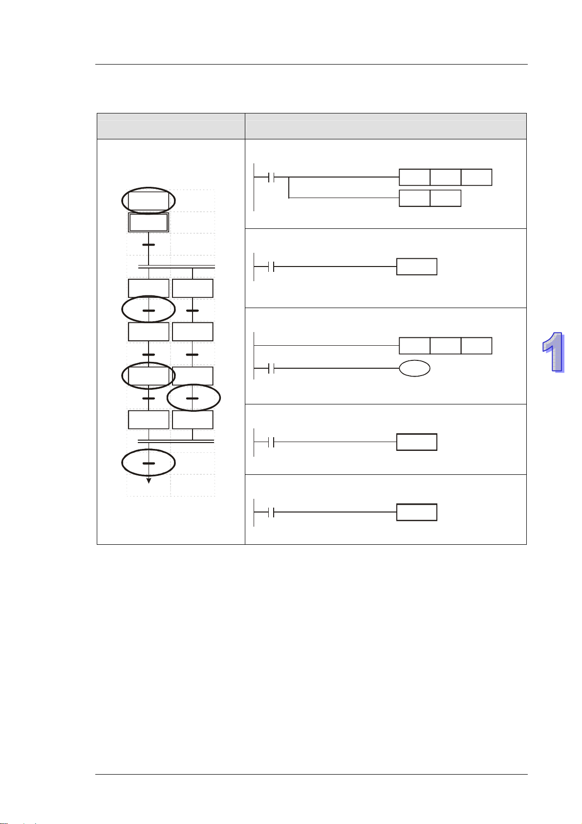
1.6 Conversion between Ladder Diagram and Instruction List Mode
Ladder Diagram
X0 X2 X1
X1
M0
M1
Y0
M2
S0
X10
S
S10
X11
S
S11
X12
S
S20
X0
C0
S12SS13
S
X1
X1
M2
Instruction
LD X0
Y0
C0
SET S0
OR X1
LD X2
OR M0
ORI M1
ANB
LD M2
AND Y0
ORB
AN I X1
10
OUT Y0
AND C0
SET S10
SET S0
STL S0
LD X10
11
SET S11
OUT Y10
SET S1 0
STL S10
LD X11
SET S12
OUT Y11
SET S11
SET S13
SET S1 2
SET S1 3
STL S11
12
LD X12
OUT Y12
SET S20
SET S2 0
STL S20
X13
S
S0
RET
STL S12
STL S13
LD X13
OUT S0
RET
CNT
C0
LD X0
K10
CNT C0 K10
LD C0
M0
M1
M2
RST C0
END
MPS
AND X1
OUT M0
MRD
AN I X1
OUT M1
MPP
AN I M2
OUT M2
RST C0
END
OR
block
OR
block
Block in series
AND
block
Block in parallel
ANI
Multiple
output s
Start of step ladder
S0 status operates with X10
Output Y10 and
transfer of step point
Read S10 status
Output Y1 1 and
transfer of step points
Read S11 status
S11 operates with X12
Output Y12 and
transfer of step points
Convergence of
multip le status
Read X13 status and
transfer of step point
Retur n
Read C0
Multi ple
output s
End of program
The output
continues
based on
status of
End of step
ladder
1-11
Page 20
DVP-ES2/EX2/SS2/SA2/SX2/SE Operation Manual - Programming
1.7 Fuzzy Syntax
Generally, the ladder diagram programming is conducted according to the “up to down and left to
right” principle. However, some programming methods not following this principle still perform the
same control results. Here are some examples explaining this kind of “fuzzy syntax.”
Example 1:
X0 X2 X4
X5X3X1
Better method OK method
LD X0 LD X0
OR X1 OR X1
LD X2 LD X2
OR X3 OR X3
ANB LD X4
LD X4 OR X5
OR X5 ANB
ANB ANB
The two instruction programs can be converted into the same ladder diagram. The difference
between Better and OK method is the ANB operation conducted by MPU. ANB instruction cannot
be used continuously for more than 8 times. If more than 8 ANB instructions are used continuously,
program error will occur. Therefore, apply ANB instruction after a block is made is the better
method to prevent the possible errors. In addition, it’s also the more logical and clearer
programming method for general users.
Example 2:
X0
Good method Bad method
X1
LD X0 LD X0
OR X1 LD X1
X2
X3
OR X2 LD X2
OR X3 LD X3
ORB
ORB
ORB
The difference between Good and Bad method is very clear. With longer program code, the
required MPU operation memory increases in the Bad method. To sum up, following the general
principle and applying good / better method when editing programs prevents possible errors and
improves program execution speed as well.
Common Programming Errors
PLC processes the diagram program from up to down and left to right. When editing ladder
diagram users should adopt this principle as well otherwise an error would be detected by WPLSoft
when compiling user program. Common program errors are listed below:
1-12
Page 21
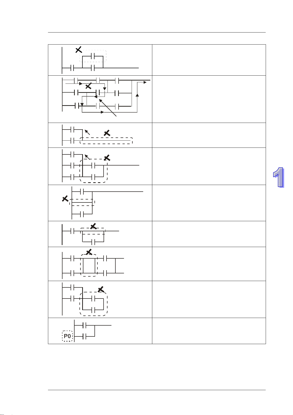
Reverse cur rent
1. PLC Concepts
OR operation upward is not allowed.
“Reverse current” exists.
Output should be connected on top of the
circuit..
Block combination should be made on top of the
circuit..
Parallel connection with empty device is not
allowed..
Parallel connection with empty device is not
allowed.
No device in the middle block.
Devices and blocks in series should be
horizontally aligned
Label P0 should be at the first row of the
complete network.
1-13
Page 22
DVP-ES2/EX2/SS2/SA2/SX2/SE Operation Manual - Programming
“Reverse current” exists
1.8 Correcting Ladder Diagram
Example 1:
Connect the block to the front for omitting ANB instruction because simplified program improves
processing speed
X0 X1
Instruction List
X2
LD X0
LD X1
OR X2
ANB
Ø
X0X1
X2
Example 2:
When a device is to be connected to a block, connect the device to upper row for omitting ORB
instruction
T0
X1
X2
Instruction List
LD X1
OR X2
AND X0
Instruction List
LD T0
LD X1
AND X2
ORB
1-14
X1
T0
X2
Ø
Instruction List
LD X1
AND X2
OR T0
Page 23
1. PLC Concepts
Example 3:
“Reverse current” existed in diagram (a) is not allowed for PLC processing principle.
X0
Instruction List
LD X0
X1
X3
X2
X4
OR X1
AND X2
LD X3
(a)
AND X4
ORB
Ø
X3
X1
X4
X2
Instruction List
LD X3
AND X4
X0
(b)
LD X1
OR X0
AND X2
ORB
Example 4:
For multiple outputs, connect the output without additional input devices to the top of the circuit for
omitting MPS and MPP instructions.
X0
Y1
Y0
Instruction List
MPS
AND X0
OUT Y1
MPP
OUT Y0
Ø
Y0
X0
Y1
Instruction List
OUT Y0
AND X0
OUT Y1
1-15
Page 24
DVP-ES2/EX2/SS2/SA2/SX2/SE Operation Manual - Programming
Example 5:
Correct the circuit of reverse current. The pointed reverse current loops are modified on the right.
X0 X1 X2
X0
X3
X6
reverse current
X4
X1
X7
X2
X5
X10
LOOP1
Ö
X3 X4 X5
X6 X7 X5
X10
X10
LOOP1
Example 6:
Correct the circuit of reverse current. The pointed reverse current loops are modified on the ri ght.
X0
X3
X6
X1
X4
X7
reverse current
X2
X5
X10
LOOP1
X0 X1 X2
X3 X4 X5
X6
X3 X7 X10
Ö
Reverse current
X0
X3
X6
X1
X4
X7
X2
X5
X10
LOOP2
X6
X0 X1 X7 X10
X4
LOOP1
LOOP
2
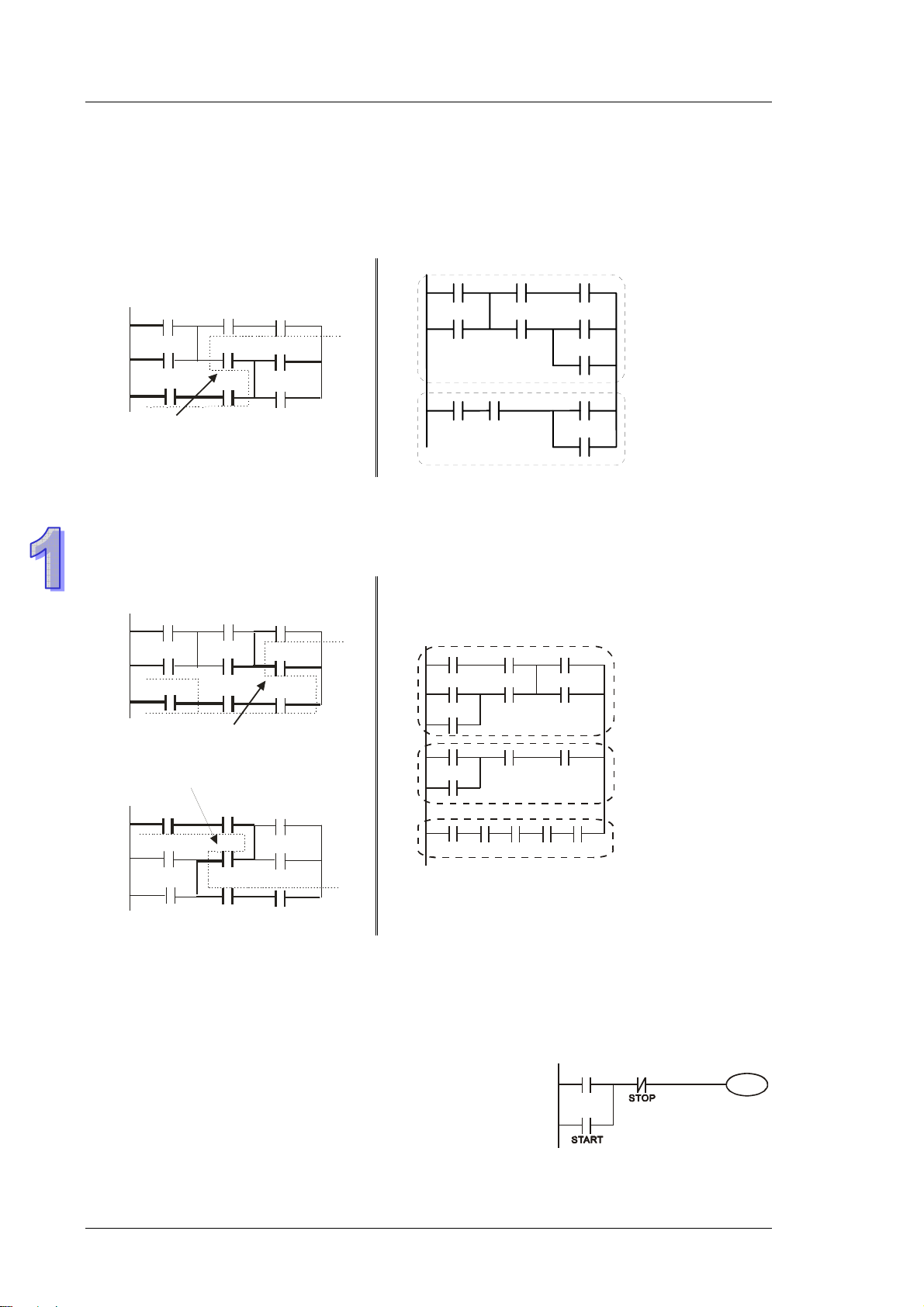
1.9 Basic Program Design Examples
Example 1 - Stop First latched circuit
When X1 (START) = ON and X2 (STOP) = OFF, Y1 will be ON.
If X2 is turned on, Y1 will be OFF. This is a Stop First circuit
because STOP button has the control pri ority than START
1-16
Y1
X1
X2
Y1
Page 25
Example 2 - Start First latched circuit
When X1 (START) = ON and X2 (STOP) = OFF, Y1 will be ON
and latched. If X2 is turned ON, Y1 remains ON. This is a Start
First circuit because START button has the control priority than
STOP
Example 3 - Latched circuit of SET and RST
The diagram opposite are latched circuits consist of RST and
SET instructions.
In PLC processing principle, the instruction close to the end of
the program determines the final output status of Y1. Therefore,
if both X1 and X2 are ON, RST which is lower than SET forms a
Stop First circuit while SET which is lower than RST forms a
Start First circuit.
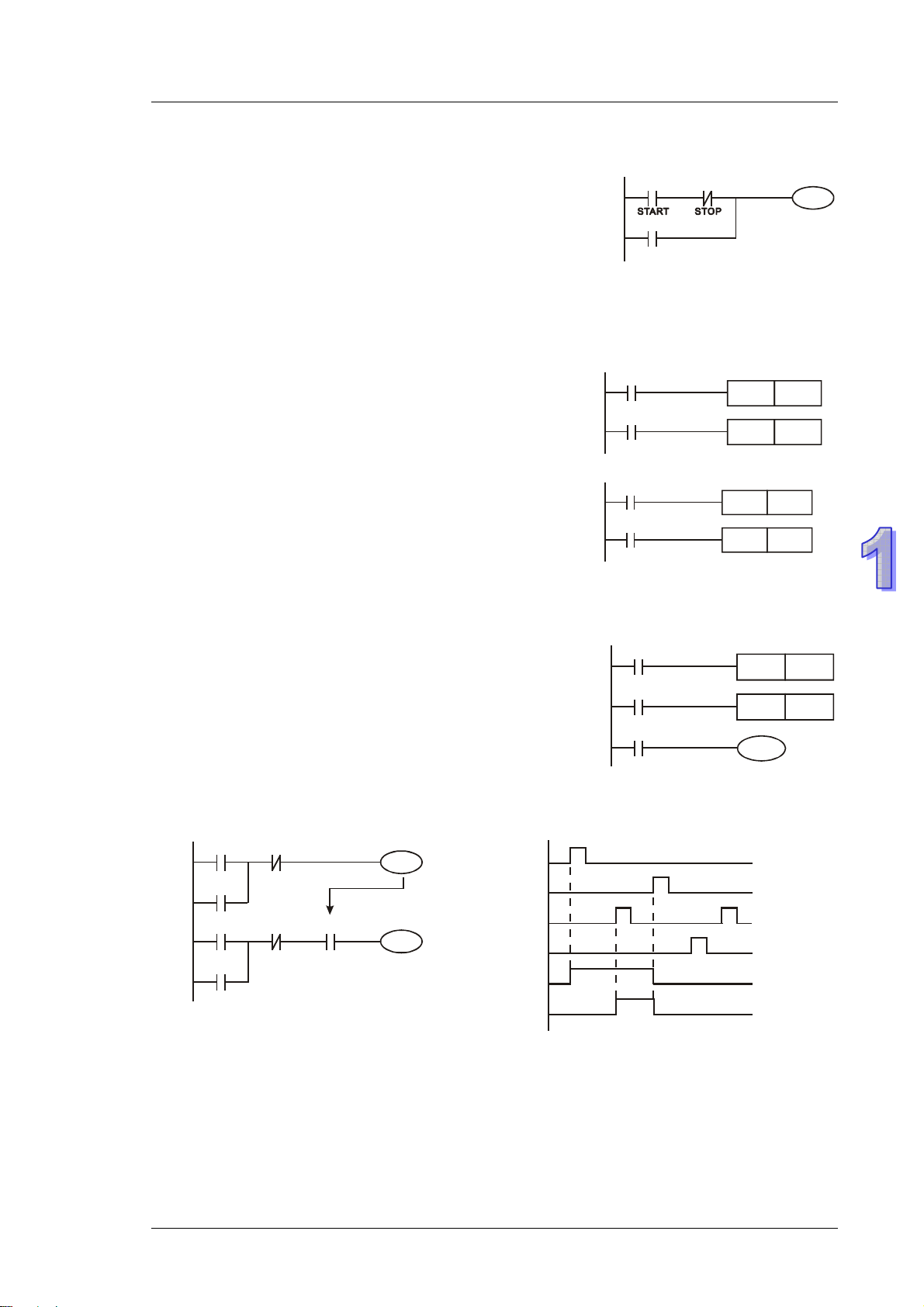
Example 4 - Power down latched circuit
The auxiliary relay M512 is a latched relay. Once X1 is ON, Y1
retains its status before power down and resumes after power
up.
X1
Y1
Stop first
X1
X2
Start first
X2
X1
X1
X2
M512
1. PLC Concepts
X2
Y1
SET
RST
Y1
Y1
RST
SET
Y1
Y1
M512
SET
RST M 5 12
Y1
Example 5 - Conditional Control
X1
Y1
X2
Y2
X3
X4
Y1
Y1
Y2
X1
X3
X2
X4
Y1
Y2
Because NO contact Y1 is connected to the circuit of Y2 output, Y1 becomes one of the conditions
for enabling Y2, i.e. for turning on Y2, Y1 has to be ON
1-17
Page 26
DVP-ES2/EX2/SS2/SA2/SX2/SE Operation Manual - Programming
Example 6- Interlock control
X1
Y1
X3
Y2
Y1
X1
X3
X2
X2
Y2
X4
Y1
Y2
X4
Y1
Y2
NC contact Y1 is connected to Y2 output circuit and NC contact Y2 is connected Y1 output circuit.
If Y1 is ON, Y2 will definitely be OFF and vice versa. This forms an Interlock circuit which prevents
both outputs to be ON at the same time. Even if both X1 and X2 are ON, in this case only Y1 will
be enabled.
Example 7 - Sequential Control
X1
Y1
X3
Y2
Y1
Connect NC contact Y2 to Y1 output circuit and
NO contact Y1 to Y2 output circuit. Y1 becomes
one of the conditions to turn on Y2. In addition, Y1
X2
Y2
X4
Y1
Y2
will be OFF when Y2 is ON, which forms an
sequential control process.
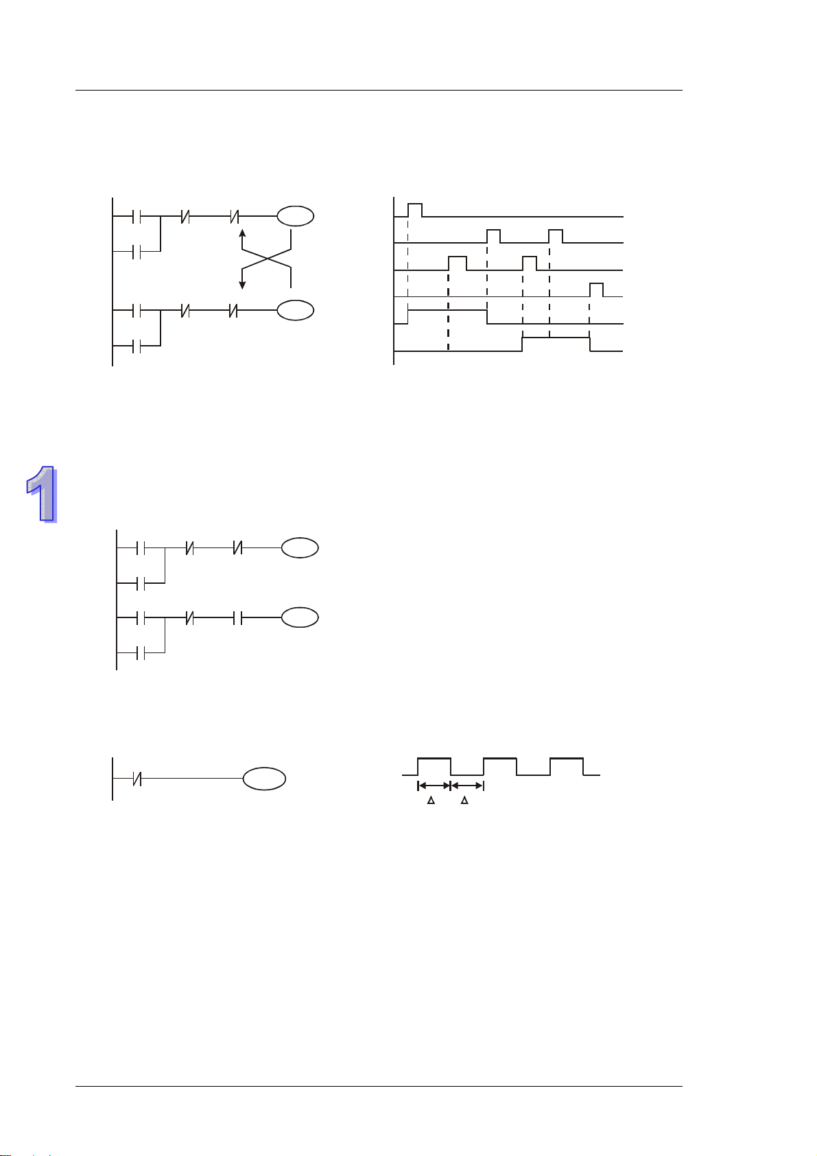
Example 8 - Oscillating Circuit
An oscillating circuit with cycle ΔT+ΔT
Y1
Y1
Y1
T T
In the first scan, Y1 turns on. In the second scan, Y1 turns off due to the reversed state of contact
Y1. Y1 output status changes in every scan and forms an oscillating circuit with output cycleΔ
T(ON)+ΔT(OFF)
1-18
Page 27
Example 9 – Oscillating Circuit with Timer
An oscillating circuit with cycle nT+ΔT
1. PLC Concepts
X0
Y1
TMR
T0
Kn
X0
T0
Y1
Y1
TTn
When X0 = ON, T0 starts timing (nT). Once the set time is reached, contact T0 = ON to enable
Y1(ΔT). In next scan, Timer T0 is reset due to the reversed status of contact Y1. Therefore contact
T0 is reset and Y1 = OFF. In next scan, T0 starts timing again. The process forms an oscillating
circuit with output cycle nT+ΔT.
Example 10 - Flashing Circuit
The ladder diagram uses two timers to form an oscillating circuit which enables a flashing indicator
or a buzzing alarm. n1 and n2 refer to the set values in T1 and T2 and T refers to timer resolution.
X0
T1
X0 T1
T2
TMR
Y1
T1
Kn1
T2TMR Kn2
X0
Tn2
Y1
T
n1
Example 11 - Trigger Circuit
In this diagram, rising-edge contact X0 generates trigger pulses to control two actions executing
interchangeably.
X0
X0
T
M0
Y1
M0
M0
M0
Y1
Y1
Y1
Example 12 - Delay OFF Circuit
If X0 = ON, timer T10 is not energized but coil Y1 is ON. When X0 is OFF, T10 is activated. After
100 seconds (K1000 × 0.1 sec = 100 sec), NC contact T10 is ON to turn off Y1. Turn-off action is
delayed for 100 seconds by this delay OFF circuit.
X0
T10
TMR
Y1
T10
K1000
X0
Y1
Timer Resolution: 0.1 sec
100 seconds
1-19
Page 28
DVP-ES2/EX2/SS2/SA2/SX2/SE Operation Manual - Programming
Example 13 - Output delay circuit
The output delay circuit is composed of two timers executing delay actions. No matter input X0 is
ON or OFF, output Y4 will be delayed.
X0
T5
K50
5 secs
T5
T5
Y4
TMR
T6
Y4
Y4
X0
TMR
T6
K30
Example 14 -
Timing extension circuit
X0
TMR
T11
T12
T11
T12TMR Kn2
Y1
.
Kn1
The total delay time: (n1+n2)* T. T refers to the
timer resolution.
Timer = T11, T12
Timer resolution: T
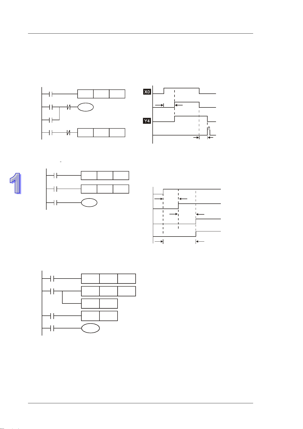
Example 15 – Counting Range Extension Circuit
X13
The counting range of a 16-bit counter is 0 ~
32,767. The opposite circuit uses two counters to
increase the counting range as n1*n2. When
value in counter C6 reaches n2, The pulses
counted from X13 will be n1*n2.
C5
X14
C6
CNT
RST
Y1
C5
Kn1
C6CNT Kn 2
C5RST
C6
T6
X0
T11
T12
Y1
n1*
T
(n1+n2)*
n2*
T
3 secs
T
T
1-20
Page 29
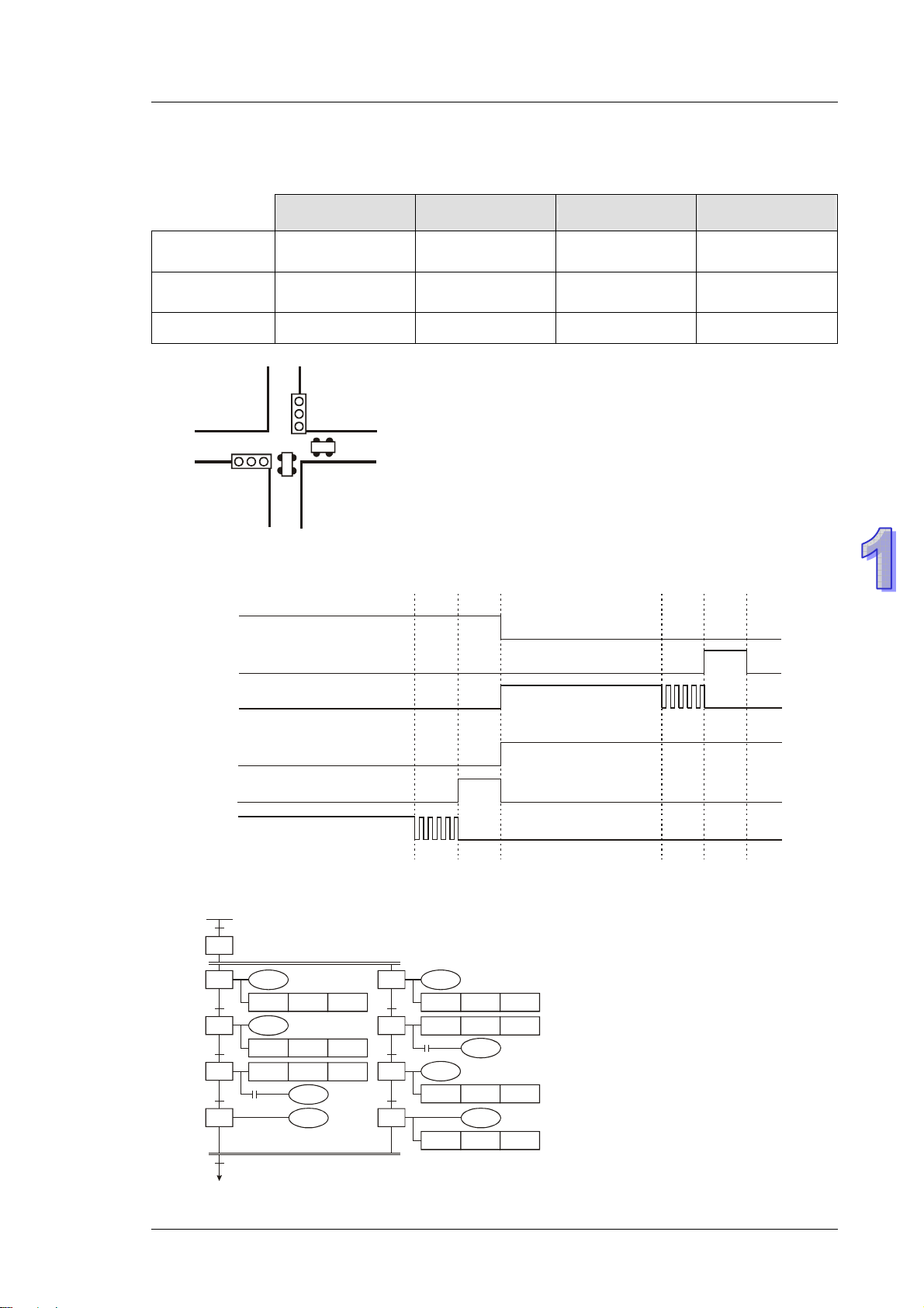
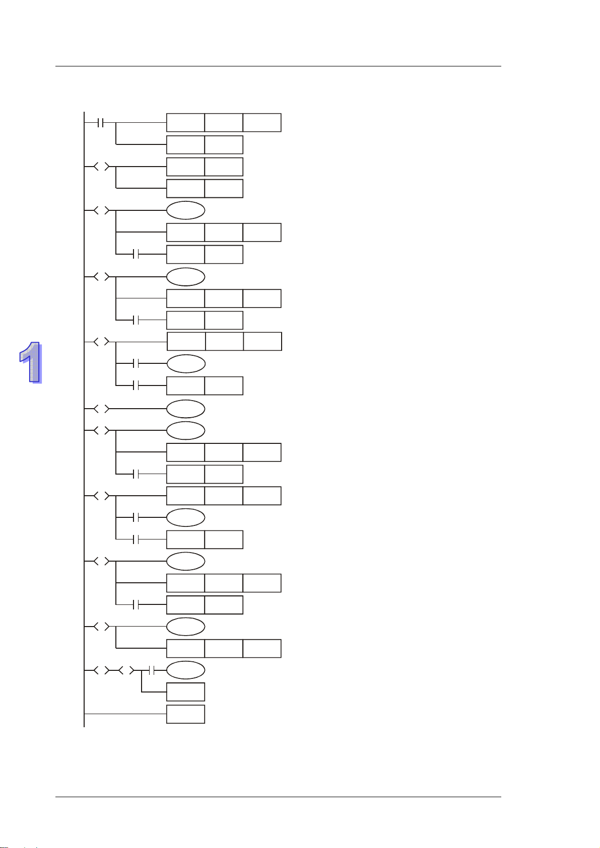
Example 16 - Traffic light control (Step Ladder Logic)
Traffic light control
1. PLC Concepts
Red light Yellow light Green light
Green light
blinking
Vertical light Y0 Y1 Y2 Y2
Horizontal light Y20 Y21 Y22 Y22
Light Time 35 Sec 5 Sec 25 Sec 5 Sec
Vertical
Light
Horizontal
Light
Timing Diagram:
Vertical
Light
Red
Y0
Y1
Yellow
Green
Y2
Horizontal
Light
Red
Y20
Yellow
Y21
Green
Y22
SFC Figure:
M1002
S0
S20
T0
S21
T1
S22
T2
S23
T13
S0
25 Sec
Y0
TMR T0 K350
Y2
TMR T1 K250
TMR T2 K50
M1013
Y2
Y1
T10
T11
T12
S30
S31
S32
S33
5 Sec
5 Sec
Y22
TMR T10 K250
TMR T11 K50
M1013
Y22
Y21
TMR T12 K50
Y20
TMR T13 K350
25 Sec
5 Se c5 Sec
1-21
Page 30
DVP-ES2/EX2/SS2/SA2/SX2/SE Operation Manual - Programming
2
Ladder Diagram:
M100
S0
S
S20
S
S21
S
S22
S
S23
S
S30
S
T0
T1
M1013
T2
ZRST S0 S127
SET S0
SET S20
SET S30
Y0
TMR T0
K350
SET S21
Y2
TMR T1
K250
SET S22
TMR T2
K50
Y2
SET S23
Y1
Y22
S31
S
M1013
S32
S
S33
S
S23SS33
S
T10
T11
T12
TMR T10
SET S31
TMR T11
Y22
SET S32
Y21
TMR T12
SET S33
Y20
TMR T13 K350
T13
S0
RET
END
K250
K50
K50
1-22
Page 31
WPLSoft programming (SFC mode)
SFC logic Internal Ladder Logic
LAD-0
1. PLC Concepts
M1002
S0ZRST S127
LAD-0
S0
0
S20
1
S21
2
S22
3
S23
4
S30
S31
S32
S33
SET
S0
Transfer con dition 1
T0
TRANS*
5
6
S22
T2TMR K50
M1013
Y2
7
Transfer con dition 4
T13
T13
T13
T13
T13
T13
T13
TRANS*
TRANS*
TRANS*
TRANS*
TRANS*
TRANS*
TRANS*
S0
T12
T12
T12
T12
T12
T12
T12
TRANS*
TRANS*
TRANS*
TRANS*
TRANS*
TRANS*
TRANS*
Transfer con dition 7
1-23
Page 32

DVP-ES2/EX2/SS2/SA2/SX2/SE Operation Manual - Programming
MEMO
1-24
Page 33

Programming Concepts
DVP-ES2/EX2/SS/SA2/SX2/SE is a programmable logic controller spanning an I/O range of
10–256 I/O points (SS2/SA2/SX2/SE: 512 points). PLC can control a wide variety of devices
to solve your automation needs. PLC monitors inputs and modifies outputs as controlled
by the user program. User program provides features such as boolean logic, counting,
timing, complex math operations, and communications to other communicating products.
Chapter Contents
2.1 ES2/EX2 Memory Map.............................................................................................................. 2-2
2.2 SS2 Memory Map...................................................................................................................... 2-5
2.3 SA2 Memory Map...................................................................................................................... 2-8
2.4 SX2 Memory Map.................................................................................................................... 2-11
2.5 Status and Allocation of Latched Memory........................................................................... 2-14
2.6 PLC Bits, Nibbles, Bytes, Words, etc ...................................................................................2-15
2.7 Binary, Octal, Decimal, BCD, Hex ......................................................................................... 2-15
2.8 M Relay ....................................................................................................................................2-17
2.9 S Relay.....................................................................................................................................2-30
2.10 T (Timer) .................................................................................................................................. 2-30
2.11 C (Counter).............................................................................................................................. 2-31
2.12 High-speed Counters ............................................................................................................. 2-34
2.13 Special Data Register............................................................................................................. 2-39
2.14 E, F Index Registers ............................................................................................................... 2-51
2.15 Nest Level Pointer[N], Pointer[P], Interrupt Pointer [I] .......................................................2-51
2.16 Applications of Special M Relays and D Registers.............................................................2-55
2-1
Page 34

DVP-ES2/EX2/SS2/SA2/SX2/SE Operation Manual - Programming
A
2.1 ES2/EX2 Memory Map
Specifications
Control Method Stored program, cyclic scan system
I/O Processing Method
Batch processing method (when END instruction is
executed)
Execution Speed LD instructions – 0.54μs, MOV instructions – 3.4μs
Program language Instruction List + Ladder + SFC
Program Capacity 15872 steps
Bit
Contacts
X External inputs
Y External outputs
X0~X377, octal number system, 256
points max, (*4)
Y0~Y377, octal number system, 256
points max, (*4)
Total
256+16 I/O
M0~M511, 512 points, (*1)
General
M768~M999, 232 points, (*1)
M2000~M2047, 48 points, (*1)
M
uxiliary
relay
Latched
Special
M512~M767, 256 points, (*2)
M2048~M4095, 2048 points, (*2)
M1000~M1999, 1000 points, some
are latched
Total
4096 points
T0~T126, 127 points, (*1)
100ms
(M1028=ON,
T64~T126:
10ms)
T Timer
10ms
(M1038=ON,
T200~T245: 1ms)
T128~T183, 56 points, (*1)
T184~T199 for Subroutines, 16
points, (*1)
T250~T255(accumulative),
6 points (*1)
T200~T239, 40 points, (*1)
T240~T245(accumulative),
Total
256 points
6 points, (*1)
T127, 1 points, (*1)
1ms
T246~T249(accumulative), 4 points,
(*1)
C
Counter
16-bit count up
C0~C111, 112 points, (*1)
C128~C199,72 points, (*1)
C112~C127,16 points, (*2)
Total
232 points
C200~C223, 24 points, (*1)
C224~C231, 8 points, (*2)
2-2
32-bit count
up/down
Page 35

Specifications
C235~C242, 1 phase 1 input, 8
points, (*2)
C232~C234, 2 phase 2 input, 3
points, (*2)
C243~C244, 1 phase 1 input, 2
points, (*2)
C245~C250, 1 phase 2 input, 6
points, (*2)
32bit
highspeed
count
up/down
Software
Hard-
ware
C251~C254 2 phase 2 input, 4
points, (*2)
Initial step point S0~S9, 10 points, (*2)
2. Programming Concepts
Total
23 points
Word
Register
S10~S19, 10 points (use with IST
instruction), (*2)
S
Step
point
Zero point return
Latched S20~S127, 1 08 points, (*2)
General S128~S911, 784 points, (*1)
Alarm S912~S1023, 112 points, (*2)
T Current value T0~T255, 256 words
C0~C199, 16-bit counter, 200 words
C Current value
C200~C254, 32-bit counter, 55 words
D0~D407, 408 words, (*1)
General
D600~D999, 400 words, (*1)
D3920~D9999, 6080 words, (*1)
D408~D599, 192 words, (*2)
D2000~D3919, 1920 words, (*2)
D1000~D1999, 1000 words, some
are latched
D9900~D9999,100 words , (*1),
(*5)
Data
D
register
Latched
Special
For Special
mudules
Total 1024
points
Total
10000 points
Pointer
Index E0~E7, F0~F7, 16 words, (*1)
N Master control loop N0~N7, 8 points
P Pointer P0~P255, 256 points
I Interrupt
Service
External interrupt
I000/I001(X0), I100/I101(X1), I200/I201(X2),
I300/I301(X3), I400/I401(X4), I500/I501(X5),
I600/I601(X6), I700/I701(X7), 8 points (01: risingedge trigger
, 00: falling-edge trigger )
2-3
Page 36

DVP-ES2/EX2/SS2/SA2/SX2/SE Operation Manual - Programming
Specifications
Timer interrupt
High-speed
counter interrupt
Communication
interrupt
I602~I699, I702~I799, 2 points (T imer resolution =
1ms)
I010, I020, I030, I040, I050, I060, I070, I080,8
points
I140(COM1), I150(COM2), I160(COM3), 3 points,
(*3)
K-32,768 ~ K32,767 (16-bit operation),
K Decimal K-2,147,483,648 ~ K2,147,483,647 (32-bit
Constant
H Hexadecimal
operation)
H0000 ~ HFFFF (16-bit operation),
H00000000 ~HFFFFFFFF (32-bit operation)
COM1: built-in RS-232 ((Master/Slave)
Serial ports
COM2: built-in RS-485 (Master/Slave)
COM3: built-in RS-485 (Master/Slave)
COM1 is typically the programming port.
Real Time Clock Year, Month, Day, Week, Hours, Minutes, Seconds
Special I/O Modules Up to 8 special I/O modules can be connected
Notes:
1. Non-latched area cannot be modified
2. Latched area cannot be modified
3. COM1: built-in RS232 port. COM2: built-in RS485 port. COM3: built-in RS485 port.
4. When input points(X) are expanded to 256 points, only 16 output points(Y) are applicable. Also,
when ouput points(Y) are expanded to 256 points, only 16 input points(X) are applicable.
5. This area is applicable only when the ES2/EX2 MPU is connected with special I/O modules.
Every special I/O module occupies 10 points.
2-4
Page 37

2. Programming Concepts
A
2.2 SS2 Memory Map
Specifications
Control Method Stored program, cyclic scan system
I/O Processing Method
Batch processing method (when END instruction is
executed)
Execution Speed LD instructions – 0.54μs, MOV instructions – 3.4μs
Program language Instruction List + Ladder + SFC
Program Capacity 7920 steps
Bit
Contacts
X External inputs
Y External outputs
X0~X377, octal number system, 256
points max.
Y0~Y377, octal number system, 256
points max.
Total
480+14
I/O(*4)
M0~M511, 512 points, (*1)
General
M768~M999, 232 points, (*1)
M2000~M2047, 48 points, (*1)
M
uxiliary
relay
Latched
Special
M512~M767, 256 points, (*2)
M2048~M4095, 2048 points, (*2)
M1000~M1999, 1000 points, some
are latched
Total
4096 points
T0~T126, 127 points, (*1)
100ms
(M1028=ON,
T64~T126:
10ms)
T Timer
10ms
(M1038=ON,
T200~T245: 1ms)
T128~T183, 56 points, (*1)
T184~T199 for Subroutines, 16
points, (*1)
T250~T255(accumulative),
6 points (*1)
T200~T239, 40 points, (*1)
T240~T245(accumulative),
Total
256 points
6 points, (*1)
T127, 1 points, (*1)
1ms
T246~T249(accumulative), 4 points,
(*1)
C
Counter
16-bit count up
C0~C111, 112 points, (*1)
C128~C199, 72 points, (*1)
C112~C127, 16 points, (*2)
Total
233 points
32-bit count
up/down
C200~C223, 24 points, (*1)
C224~C232, 9 points, (*2)
2-5
Page 38

DVP-ES2/EX2/SS2/SA2/SX2/SE Operation Manual - Programming
Specifications
C235~C242, 1 phase 1 input, 8
points, (*2)
C233~C234, 2 phase 2 input, 2
points, (*2)
C243~C244, 1 phase 1 input, 2
points, (*2)
C245~C250, 1 phase 2 input, 6
points, (*2)
32bit
highspeed
count
up/down
Software
Hard-
ware
C251~C254 2 phase 2 input, 4
points, (*2)
Initial step point S0~S9, 10 points, (*2)
Total
22 points
Word
Register
S10~S19, 10 points (use with IST
instruction), (*2)
S
Step
point
Zero point return
Latched S20~S127, 1 08 points, (*2)
General S128~S911, 784 points, (*1)
Alarm S912~S1023, 112 points, (*2)
T Current value T0~T255, 256 words
C0~C199, 16-bit counter, 200 words
C Current value
C200~C254, 32-bit counter, 55 words
D0~D407, 408 words, (*1)
General
D600~D999, 400 words, (*1)
D3920~D4999, 1080 words, (*1)
D
Data
register
Latched
Special
D408~D599, 192 words, (*2)
D2000~D3919, 1920 words, (*2)
D1000~D1999, 1000 words, some
are latched
Total 1024
points
Total
5016 points
Pointer
2-6
Index E0~E7, F0~F7, 16 words, (*1)
N Master control loop N0~N7, 8 points
P Pointer P0~P255, 256 points
I Interrupt
Service
External interrupt
Timer interrupt
I000/I001(X0), I100/I101(X1), I200/I201(X2),
I300/I301(X3), I400/I401(X4), I500/I501(X5),
I600/I601(X6), I700/I701(X7), 8 points (01: risingedge trigger
, 00: falling-edge trigger )
I602~I699, I702~I799, 2 points (T imer resolution =
1ms)
Page 39

Specifications
2. Programming Concepts
High-speed
counter interrupt
Communication
interrupt
I010, I020, I030, I040, I050, I060, I070, I080, 8
points
I140(COM1), I150(COM2), 2 points, (*3)
K-32,768 ~ K32,767 (16-bit operation),
K Decimal K-2,147,483,648 ~ K2,147,483,647 (32-bit
Constant
H Hexadecimal
operation)
H0000 ~ HFFFF (16-bit operation),
H00000000 ~HFFFFFFFF (32-bit operation)
COM1: built-in RS-232 ((Master/Slave)
Serial ports COM2: built-in RS-485 (Master/Slave)
COM1 is typically the programming port.
Real Time Clock Year, Month, Day, Week, Hours, Minutes, Seconds
Special I/O Modules Up to 8 special I/O modules can be connected
Notes:
1. Non-latched area cannot be modified
2. Latched area cannot be modified
3. COM1: built-in RS232 port. COM2: built-in RS485 port.
4. SS2 MPU occupies 16 input points (X0~X17) and 16 output points (Y0~Y17).
2-7
Page 40

DVP-ES2/EX2/SS2/SA2/SX2/SE Operation Manual - Programming
A
2.3 SA2 Memory Map
Specifications
Control Method Stored program, cyclic scan system
I/O Processing Method
Batch processing method (when END instruction is
executed)
Execution Speed LD instructions – 0.54μs, MOV instructions – 3.4μs
Program language Instruction List + Ladder + SFC
Program Capacity 15872 steps
Bit
Contacts
X External inputs
Y External outputs
X0~X377, octal number system, 256
points max.
Y0~Y377, octal number system, 256
points max.
Total
480+14
I/O(*4)
M0~M511, 512 points, (*1)
General
M768~M999, 232 points, (*1)
M2000~M2047, 48 points, (*1)
M
uxiliary
relay
Latched
Special
M512~M767, 256 points, (*2)
M2048~M4095, 2048 points, (*2)
M1000~M1999, 1000 points, some
are latched
Total
4096 points
T0~T126, 127 points, (*1)
100ms
(M1028=ON,
T64~T126:
10ms)
T Timer
10ms
(M1038=ON,
T200~T245: 1ms)
T128~T183, 56 points, (*1)
T184~T199 for Subroutines, 16
points, (*1)
T250~T255(accumulative),
6 points (*1)
T200~T239, 40 points, (*1)
T240~T245(accumulative),
Total
256 points
6 points, (*1)
T127, 1 points, (*1)
1ms
T246~T249(accumulative), 4 points,
(*1)
C
Counter
16-bit count up
C0~C111, 112 points, (*1)
C128~C199, 72 points, (*1)
C112~C127, 16 points, (*2)
Total
233 points
C200~C223, 24 points, (*1)
C224~C232, 9 points, (*2)
C235~C242, 1 phase 1 input, 8
points, (*2)
Total
22 points
2-8
32-bit count
up/down
32bit Softhigh- ware
Page 41
Specifications
2. Programming Concepts
speed
count
up/down
C233~C234, 2 phase 2 input, 2
points, (*2)
C243~C244, 1 phase 1 input, 2
points, (*2)
Hard-
ware
C245~C250, 1 phase 2 input, 6
points, (*2)
C251~C254 2 phase 2 input, 4
points, (*2)
Initial step point S0~S9, 10 points, (*2)
S10~S19, 10 points (use with IST
instruction), (*2)
S
Step
point
Zero point return
Latched S20~S127, 1 08 points, (*2)
General S128~S911, 784 points, (*1)
Alarm S912~S1023, 112 points, (*2)
T Current value T0~T255, 256 words
C0~C199, 16-bit counter, 200 words
C Current value
C200~C254, 32-bit counter, 55 words
Total 1024
points
Word
Register
Pointer
D0~D407, 408 words, (*1)
General
D600~D999, 400 words, (*1)
D3920~D9999, 6080 words, (*1)
Data
D
register
Latched
Special
D408~D599, 192 words, (*2)
D2000~D3919, 1920 words, (*2)
D1000~D1999, 1000 words, some
are latched
Index E0~E7, F0~F7, 16 words, (*1)
N Master control loop N0~N7, 8 points
P Pointer P0~P255, 256 points
I Interrupt
Service
External interrupt
Timer interrupt
I000/I001(X0), I100/I101(X1), I200/I201(X2),
I300/I301(X3), I400/I401(X4), I500/I501(X5),
I600/I601(X6), I700/I701(X7), 8 points (01: rising-
edge trigger
, 00: falling-edge trigger )
I602~I699, I702~I799, 2 points (T imer resolution =
1ms)
Total
10000 points
2-9
Page 42

DVP-ES2/EX2/SS2/SA2/SX2/SE Operation Manual - Programming
Specifications
High-speed
counter interrupt
Communication
interrupt
I010, I020, I030, I040, I050, I060, I070, I080, 8
points
I140(COM1), I150(COM2), I160(COM3), 3 points,
(*3)
K-32,768 ~ K32,767 (16-bit operation),
K Decimal K-2,147,483,648 ~ K2,147,483,647 (32-bit
Constant
H Hexadecimal
operation)
H0000 ~ HFFFF (16-bit operation),
H00000000 ~HFFFFFFFF (32-bit operation)
COM1: built-in RS-232 ((Master/Slave)
Serial ports
COM2: built-in RS-485 (Master/Slave)
COM3: built-in RS-485 (Master/Slave)
COM1 is typically the programming port.
Real Time Clock Year, Month, Day, Week, Hours, Minutes, Seconds
Special I/O Modules Up to 8 special I/O modules can be connected
Notes:
1. Non-latched area cannot be modified
2. Latched area cannot be modified
3. COM1: built-in RS232 port. COM2: built-in RS485 port. COM3: built-in RS-485 port
4. SA2 MPU occupies 16 input points (X0~X17) and 16 output points (Y0~Y17).
2-10
Page 43

2. Programming Concepts
A
2.4 SX2 Memory Map
Specifications
Control Method Stored program, cyclic scan system
I/O Processing Method
Batch processing method (when END instruction is
executed)
Execution Speed LD instructions – 0.54μs, MOV instructions – 3.4μs
Program language Instruction List + Ladder + SFC
Program Capacity 15872 steps
Bit
Contacts
X External inputs
Y External outputs
X0~X377, octal number system, 256
points max.
Y0~Y377, octal number system, 256
points max.
Total
480+14
I/O(*4)
M0~M511, 512 points, (*1)
General
M768~M999, 232 points, (*1)
M2000~M2047, 48 points, (*1)
M
uxiliary
relay
Latched
Special
M512~M767, 256 points, (*2)
M2048~M4095, 2048 points, (*2)
M1000~M1999, 1000 points, some
are latched
Total
4096 points
T0~T126, 127 points, (*1)
100ms
(M1028=ON,
T64~T126:
10ms)
T Timer
10ms
(M1038=ON,
T200~T245: 1ms)
T128~T183, 56 points, (*1)
T184~T199 for Subroutines, 16
points, (*1)
T250~T255(accumulative),
6 points (*1)
T200~T239, 40 points, (*1)
T240~T245(accumulative),
Total
256 points
6 points, (*1)
T127, 1 points, (*1)
1ms
T246~T249(accumulative), 4 points,
(*1)
C
Counter
16-bit count up
C0~C111, 112 points, (*1)
C128~C199, 72 points, (*1)
C112~C127, 16 points, (*2)
Total
232 points
32-bit count
up/down
32bit Softhigh- ware
C200~C223, 24 points, (*1)
C224~C231, 8 points, (*2)
C235~C242, 1 phase 1 input, 8
points, (*2)
Total
23 points
2-11
Page 44

DVP-ES2/EX2/SS2/SA2/SX2/SE Operation Manual - Programming
Specifications
speed
count
up/down
C232~C234, 2 phase 2 input, 2
points, (*2)
C243~C244, 1 phase 1 input, 2
points, (*2)
Hard-
ware
C245~C250, 1 phase 2 input, 6
points, (*2)
C251~C254 2 phase 2 input, 4
points, (*2)
Initial step point S0~S9, 10 points, (*2)
S10~S19, 10 points (use with IST
instruction), (*2)
S
Step
point
Zero point return
Latched S20~S127, 1 08 points, (*2)
General S128~S911, 784 points, (*1)
Alarm S912~S1023, 112 points, (*2)
T Current value T0~T255, 256 words
C0~C199, 16-bit counter, 200 words
C Current value
C200~C254, 32-bit counter, 55 words
Total 1024
points
Word
Register
Pointer
D0~D407, 408 words, (*1)
General
D600~D999, 400 words, (*1)
D3920~D9999, 6080 words, (*1)
D
Data
register
Latched
Special
D408~D599, 192 words, (*2)
D2000~D3919, 1920 words, (*2)
D1000~D1999, 1000 words, some
are latched
Index E0~E7, F0~F7, 16 words, (*1)
N Master control loop N0~N7, 8 points
P Pointer P0~P255, 256 points
I Interrupt
Service
External interrupt
Timer interrupt
I000/I001(X0), I100/I101(X1), I200/I201(X2),
I300/I301(X3), I400/I401(X4), I500/I501(X5),
I600/I601(X6), I700/I701(X7), 8 points (01: risingedge trigger
, 00: falling-edge trigger )
I602~I699, I702~I799, 2 points (T imer resolution =
1ms)
Total
10000 points
2-12
Page 45

Specifications
2. Programming Concepts
High-speed
counter interrupt
Communication
interrupt
I010, I020, I030, I040, I050, I060, I070, I080, 8
points
I140(COM1), I150(COM2), 2 points, (*3)
K-32,768 ~ K32,767 (16-bit operation),
K Decimal K-2,147,483,648 ~ K2,147,483,647 (32-bit
Constant
H Hexadecimal
operation)
H0000 ~ HFFFF (16-bit operation),
H00000000 ~HFFFFFFFF (32-bit operation)
COM1: built-in RS-232 ((Master/Slave)
Serial ports
COM2: built-in RS-485 (Master/Slave)
COM3: built-in USB port (Slave)
COM1 is typically the programming port.
Real Time Clock Year, Month, Day, Week, Hours, Minutes, Seconds
Right side: Up to 8 special I/O modules can be
Special I/O Modules
connected
Left side: Up to 8 high-speed I/O modules can be
connected
Notes:
1. Non-latched area cannot be modified
2. Latched area cannot be modified
3. COM1: built-in RS232 port. COM2: built-in RS485 port.
4. SX2 MPU occupies 16 input points (X0~X17) and 16 output points (Y0~Y17).
2-13
Page 46

DVP-ES2/EX2/SS2/SA2/SX2/SE Operation Manual - Programming
2.5 Status and Allocation of Latched Memory
Clear all
Memory
type
Nonlatched
Latched Unchanged Unchanged Clear 0
Special M,
Special D,
Index
Register
Power
OFF=>ON
Clear Unchanged Clear Unchanged 0
Initial Unchanged Unchanged
STOP=>RUN
RUN=>STOP
When
M1033=OFF, clear
When M1033=ON,
No change
non-latched Factory
area setting
(M1031=ON)
Clear all
latched area
(M1032=ON)
Initial
setting
General Latched Special auxiliary relay
M
Auxiliary relay
M0~M511
M768~M999
M2000~M2047
Not latched Latched
M512~M999
M2048~M4095
M1000~M1999
Some are latched and
can’t be changed.
T
Timer
C
Counter
S
Step relay
D
Register
100 ms 100 ms 1 ms 10 ms 10ms 1 ms 100 ms
T0 ~T126 T250~T
T128~T183
M1028=1,T64~
T126:10ms
non-latched non-latched Accumulative non-latched
16-bit count up 32-bit count up/down
C0~C111
C128~C199
Non-latched Latched Non-latched Latched Latched
Initial Zero return Latched General Step alarm
S0~S9 S10~S19 S20~S127 S128~S911 S912~S1023
General Latched Special register For AIO
D0~D407
D600~D999
D3920~D9899
Non-latched Latched
T184~T199 T127 T200~T239 T240~T245 T246~T249
For
subroutine
C112~C127 C200~C223 C224~C231 C232~C254
Latched Non-latched Latched
D408~D599 D9900~D999
D2000~D3919
M1038=1,T200~T245:
1ms
D1000~D1999
Some are latched, and
can’t be changed
32-bit high-speed
count up/down
Non-latched
255
-
9
2-14
Page 47

2. Programming Concepts
2.6 PLC Bits, Nibbles, Bytes, Words, etc
For different control purposes, there are five types of values inside DVP-PLC for executin g the
operations.
Numeric Description
Bit
Nibble
Bit is the basic unit of a binary number system. Range is 0 or 1
Consists of 4 consecutive bits, e.g. b3~b0. Range 0 ~ 9 in Decimal or 0~F in
Hex
Byte
Word
Consists of 2 consecutive nibbles, e.g. b7~b0. Range 00 ~ FF in Hex
Consists of 2 consecutive bytes, e.g. b15~b0. Range 0000 ~ FFFF in Hex
Consists of 2 consecutive words, e.g. b31~b1. Range 00000000 - FFFFFFFF
Double Word
in Hex
Bit, nibble, byte, word, and double word in a binary system:
DW
W1
BY3 BY2 BY1 BY0
2.7 Binary, Octal, Decimal, BCD, Hex
W0
Double Word
Word
Byte
NB0NB1NB2NB3NB4NB5NB6NB7
Nibble
Bit
For fulllfilling different kinds of internal manipulation, DVP-PLC appies 5 foramts of number systems.
Each number system has its specific purpose and function describ ed as below.
1. Binary Number, (BIN)
PLC internally calculates, operates, and stores the value in Binary format.
2. Octal Number, (OCT)
The external I/O points of DVP-PLC are numbered in octal format.
e.g.
External inputs: X0~X7, X10~X17, …, X377. (No. of device)
External outputs: Y0~Y7, Y10~Y17, …, Y377. (No. of device)
3. Decimal Number, (DEC)
DVP-PLC appies decimal operation in situations below:
z Set value for timers and counters, e.g. TMR C0 K50. (K value)
z No. of S, M, T, C, D, E, F, P, I devices, e.g. M10, T30. (No. of device)
z For use of operand in API instru ctions, e.g. MOV K123 D0. (K value)
2-15
Page 48

DVP-ES2/EX2/SS2/SA2/SX2/SE Operation Manual - Programming
z Constant K:
Decimal value in PLC operation is attached with an “K”, e.g. K100 indicates the value 100 in
Decimal format.
Exception:
When constant K is used with bit devices X, Y, M, S, the value specifed after K indicates
the groups of 4-bit unit, which forms a digit(4-bit), byte(8 bit), word(16bit), or double
word(32-bit) data, e.g. K2Y10, K4M100, representing Y10 ~ Y17 and M100~M1 15.
4. BCD (Binary Coded Decimal)
BCD format takes 1 digit or 4 bits to indicate a Decimal value, so that data of consecutive 16
bits indicates a 4-digit decimal value. Used mainly for reading values from DIP switches or
sending data to 7-segement displays
5. Hexadecimal Number, HEX
DVP-PLC appies Hexadecimal operation in situations below:
z For use of operand in API instru ctions, e.g. MOV H1A2B D0。(H value)
z Constant H:
Hexadecimal value in PLC operation is attached with an “H”, e.g. H100 indicates the value
100 in Hex format.
Reference Table:
Binary Octal Decimal (K) BCD Hexadecimal (H)
(BIN) (OCT) (DEC) (Binary Code Decimal) (HEX)
For PLC
internal
operation
No. of X, Y
relay
Costant K, No. of
registers M, S, T, C,
D, E, F, P, I devices
For DIP Switch and 7segment display
Constant H
0000 0 0 0000 0
0001 1 1 0001 1
0010 2 2 0010 2
0011 3 3 0011 3
0100 4 4 0100 4
0101 5 5 0101 5
0110 6 6 0110 6
0111 7 7 0111 7
1000 10 8 1000 8
1001 11 9 1001 9
1010 12 10 0000 A
1011 13 11 0001 B
1100 14 12 0010 C
2-16
Page 49

2. Programming Concepts
Binary Octal Decimal (K) BCD Hexadecimal (H)
(BIN) (OCT) (DEC) (Binary Code Decimal) (HEX)
For PLC
internal
operation
No. of X, Y
relay
Costant K, No. of
registers M, S, T, C,
D, E, F, P, I devices
For DIP Switch and 7segment display
Constant H
1101 15 13 0011 D
1110 16 14 0100 E
1111 17 15 0101 F
10000 20 16 0110 10
10001 21 17 0111 11
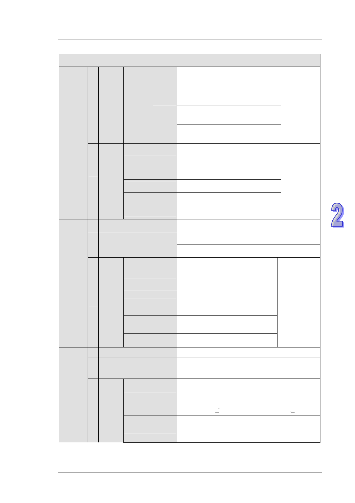
2.8 M Relay
The types and functions of special auxiliary relays (special M) are listed in the table below. Care
should be taken that some devices of the same No. may bear different meanings in different series
MPUs. Special M and special D marked with “*” will be further illustrated in 2.13. Columns marked
with “R” refers to “read only”, “R/W” refers to “read and write”, “-“ refers to the status remains
unchanged and “#” refers to that system will set it up according to the status of the PLC.
OFF
Special
M
Function
ES2
SS2 SA2 SX2
EX2
Ø
ON
STOP
RUN
Ø
RUN
Ø
STOP
Attrib.
Latch
-ed
Default
M1000* OFF ON OFF R NO OFF
M1001* ON OFF ON R NO ON
M1002*
M1003*
M1004* ON when syntax errors occur OFF OFF - R NO OFF
M1008* OFF OFF - R NO OFF
M1009
M1011* 10ms clock pulse, 5ms ON/5ms OFF OFF - - R NO OFF
M1012*
M1013* 1s clock pulse, 0.5s ON / 0.5s OFF OFF - - R NO OFF
M1014* 1 min clock pulse, 30s ON / 30s OFF OFF - - R NO OFF
M1015* Enable high-speed timer OFF - - R/W NO OFF
M1016* OFF - - R/W NO OFF
Monitor normally open contact
Monitor normally closed contact
Enable single positive pulse at the
moment when RUN is activate (Normally
OFF)
Enable single negative pulse at the
moment when RUN is activate (Normally
ON)
Watchdog timer (ON: PLC WDT time out)
Indicate LV signal due to 24VDC
insufficiency
100ms clock pulse, 50ms ON / 50ms
OFF
Indicate Year display mode of RTC.
○ ○ ○ ○
○ ○ ○ ○
○ ○ ○ ○
○ ○ ○ ○
○ ○ ○ ○
○ ○ ○ ○
○ ○ ○ ○
○ ○ ○ ○
○ ○ ○ ○
○ ○ ○ ○
○ ○ ○ ○
○ ○ ○ ○
○ ○ ○ ○
OFF ON OFF R NO OFF
ON OFF ON R NO ON
OFF - - R NO OFF
OFF - - R NO OFF
M1017* OFF - - R/W NO OFF
M1018 Flag for Radian/Degree, ON for degree OFF - - R/W NO OFF
±30 seconds correction on real time clock
○ ○ ○ ○
○ ○ ○ ○
2-17
Page 50

DVP-ES2/EX2/SS2/SA2/SX2/SE Operation Manual - Programming
OFF
Special
M
Function
ES2
SS2 SA2 SX2
EX2
Ø
ON
STOP
Ø
RUN
STOP
RUN
Ø
Attrib.
Latch
-ed
Default
M1020 Zero flag
M1021 Borrow flag
M1022 Carry flag
M1024 COM1 monitor request
M1025*
M1026 RAMP mode selection
M1027 PR output mode selection (8/16 bytes)
M1028
M1029*
M1030*
M1031* Clear all non-latched memory
M1032* Clear all latched memory
M1033* Output state latched at STOP
M1034* Disable all Y outputs
Indicate incorrect request for
communication
Switch T64~T126 timer resulotion
(10ms/100ms). ON =10ms
CH0 (Y0, Y1) pulse output execution
completed.
Pulse output Y1 execution completed
○ ○ ○ ○
○ ○ ○ ○
○ ○ ○ ○
○ ○ ○ ○
○ ○ ○ ○
○ ○ ○ ○
○ ○ ○ ○
○ ○ ○ ○
○ ○ ○ ○
○ ○ ○ ○
○ ○ ○ ○
○ ○ ○ ○
○ ○ ○ ○
○ ○ ○ ○
OFF - - R NO OFF
OFF - - R NO OFF
OFF - - R NO OFF
OFF - - R/W NO OFF
OFF - - R NO OFF
OFF - - R/W NO OFF
OFF - - R/W NO OFF
OFF - - R/W NO OFF
OFF - - R NO OFF
OFF - - R NO OFF
OFF - - R/W NO OFF
OFF - - R/W NO OFF
OFF - - R/W NO OFF
OFF - - R/W NO OFF
M1035*
M1037*
M1038
M1039* Fix scan time
M1040 Disable step transition
M1041 Step transition start
M1042 Enable pulse operation
M1043 Zero return completed
M1044 Zero point condition
M1045 Disable “all output reset” function
M1046 Indicate STL status
M1047 Enable STL monitoring
M1048 Indicate alarm status
M1049 Enable alarm monitoring
Enable X7 input point as RUN/STOP
switch
Enable 8-sets SPD function (Has to be
used with D1037)
Switch T200~T255 timer resulotion
(10ms/1ms). ON = 1ms
○ ○ ○ ○
╳ ╳ ○○
○ ○ ○ ○
○ ○ ○ ○
○ ○ ○ ○
○ ○ ○ ○
○ ○ ○ ○
○ ○ ○ ○
○ ○ ○ ○
○ ○ ○ ○
○ ○ ○ ○
○ ○ ○ ○
○ ○ ○ ○
○ ○ ○ ○
- - - R/W YES OFF
OFF OFF OFF R/W NO OFF
OFF - - R/W NO OFF
OFF - - R/W NO OFF
OFF - - R/W NO OFF
OFF - OFF R/W NO OFF
OFF - - R/W NO OFF
OFF - OFF R/W NO OFF
OFF - OFF R/W NO OFF
OFF - - R/W NO OFF
OFF - - R NO OFF
OFF - - R/W NO OFF
OFF - - R NO OFF
OFF - - R/W NO OFF
M1050 Disable interruption I000 / I001
M1051 Disable interruption I100 / I101
2-18
○ ○ ○ ○
○ ○ ○ ○
OFF - - R/W NO OFF
OFF - - R/W NO OFF
Page 51

Special
M
Function
ES2
SS2 SA2 SX2
EX2
OFF
Ø
ON
2. Programming Concepts
STOP
RUN
Ø
RUN
Ø
STOP
Attrib.
Latch
-ed
Default
M1052 Disable interruption I200 / I201
M1053 Disable interruption I300 / I301
M1054 Disable interruption I400 / I401
M1055 Disable interruption I500 / I501
M1056 Disable interruption I600~I699
M1057 Disable interruption I700~I799
M1058 COM3 monitor request
M1059
M1060 System error message 1
M1061 System error message 2
M1062 System error message 3
M1063 System error message 4
M1064 Incorrect use of operands
M1065 Syntax error
M1066 Loop error
Disable high-speed counter interruptions
I010~I080
○ ○ ○ ○
○ ○ ○ ○
○ ○ ○ ○
○ ○ ○ ○
○ ○ ○ ○
○ ○ ○ ○
○ ╳ ○ ○
○ ○ ○ ○
○ ○ ○ ○
○ ○ ○ ○
○ ○ ○ ○
○ ○ ○ ○
○ ○ ○ ○
○ ○ ○ ○
○ ○ ○ ○
OFF - - R/W NO OFF
OFF - - R/W NO OFF
OFF - - R/W NO OFF
OFF - - R/W NO OFF
OFF - - R/W NO OFF
OFF - - R/W NO OFF
OFF - - R/W NO OFF
OFF - - R/W NO OFF
OFF - - R NO OFF
OFF - - R NO OFF
OFF - - R NO OFF
OFF - - R NO OFF
OFF OFF - R NO OFF
OFF OFF - R NO OFF
OFF OFF - R NO OFF
M1067* Program execution error
M1068* Execution error locked (D1068)
M1070
M1071
M1072 PLC status (RUN/STOP), ON = RUN
M1075
M1078
M1079
M1080 COM2 monitor request
M1081
M1083*
M1084*
M1085
Switching clock pulse of Y1 for PWM
instruction (ON: 100us; OFF: 1ms)
Switching clock pulse of Y3 for PWM
instruction (ON: 100us; OFF: 1ms)
Error occurring when write in Flash ROM
Y0/CH0(Y0, Y1) pulse output pause
(immediate)
Y1 pulse output pause (immediate)
Changing conversion mode for FLT
instruction
Selecting X6 pulse-width detecting mode.
M1083 = ON, detecting pulse-width when
X6 = ON; M1083 = OFF, detecting pulsewidth when X6 = OFF.
Enabling X6 Pulse width detecting
function. (has to be used with M1183 and
D1023)
Selecting DVP-PCC01 duplicating function
○ ○ ○ ○
○ ○ ○ ○
○ ○ ○ ○
○ ○ ○ ○
○ ○ ○ ○
○ ○
○ ○ ○ ○
○ ○ ○ ○
○ ○ ○ ○
○ ○ ○ ○
○ ○ ○ ○
○ ○ ○ ○
○ ○ ○ ○
○ ○
OFF OFF - R NO OFF
OFF - - R NO OFF
OFF - - R/W NO OFF
OFF - - R/W NO OFF
OFF ON OFF R/W NO OFF
OFF - - R NO OFF
OFF OFF - R/W NO OFF
OFF OFF - R/W NO OFF
OFF - - R/W NO OFF
OFF - - R/W NO OFF
OFF - - R/W NO OFF
OFF OFF OFF R/W NO OFF
OFF - - R/W NO OFF
2-19
Page 52

DVP-ES2/EX2/SS2/SA2/SX2/SE Operation Manual - Programming
OFF
Special
M
Function
ES2
SS2 SA2 SX2
EX2
Ø
ON
STOP
Ø
RUN
STOP
RUN
Ø
Attrib.
Latch
-ed
Default
M1086
M1088
M1089
M1090
M1091
M1092
M1093
M1094
Enabling password function for DVPPCC01
Matrix comparison.
Comparing between equivalent values
(M1088 = ON) or different values (M1088
= OFF).
Indicating the end of matrix comparison.
When the comparison reaches the last bit,
M1089 = ON.
Indicating start of matrix comparison.
When the comparison starts from the first
bit, M1090 = ON.
Indicating matrix searching results. When
the comparison has matched results,
comparison will stop immediately and
M1091 = ON.
Indicating pointer error. When the pointer
Pr exceeds the comparison range, M1092
= ON
Matrix pointer increasing flag. Adding 1 to
the current value of the Pr.
Matrix pointer clear flag. Clear the current
value of the Pr to 0
○ ○ ○ ○
○ ○ ○ ○
○ ○ ○ ○
○ ○ ○ ○
○ ○ ○ ○
○ ○ ○ ○
○ ○ ○ ○
○ ○ ○ ○
OFF - - R/W NO OFF
OFF OFF - R/W NO OFF
OFF OFF - R NO OFF
OFF OFF - R NO OFF
OFF OFF - R NO OFF
OFF OFF - R NO OFF
OFF OFF - R/W NO OFF
OFF OFF - R/W NO OFF
M1095
M1096
M1097
M1098
M1099
M1102*
M1103*
M1104
M1105
M1106
M1107
Carry flag for matrix rotation / shift /
output.
Borrow flag for matrix rotation/shift/input
Direction flag for matrix
rotation/displacement
Counting the number of bits which are “1”
or “0”
ON when the bits counting result is “0”
Y2/CH1 (Y2, Y3) pulse output execution
completed
Y3 pulse output completed
Y2/CH1 (Y2, Y3) pulse output pause
(immediate)
Y3 pulse output pause (immediate)
Zero point selection. M1106=ON, change
the zero point to the right of DOG switch
for zero return on CH0.
Zero point selection. M1107=ON, change
the zero point to the right of DOG switch
for zero return on CH1.
○ ○ ○ ○
○ ○ ○ ○
○ ○ ○ ○
○ ○ ○ ○
○ ○ ○ ○
○ ○ ○ ○
○ ○ ○ ○
○ ○ ○ ○
○ ○ ○ ○
○ ○ ○ ○
○ ○ ○ ○
OFF OFF - R NO OFF
OFF OFF - R/W NO OFF
OFF OFF - R/W NO OFF
OFF OFF - R/W NO OFF
OFF OFF - R/W NO OFF
OFF - - R/W NO OFF
OFF - - R/W NO OFF
OFF OFF - R/W NO OFF
OFF OFF - R/W NO OFF
OFF OFF - R/W NO OFF
OFF OFF - R/W NO OFF
M1108
2-20
Y0/CH0 (Y0, Y1) pulse output pause
(ramp down)
○ ○ ○ ○
OFF OFF - R/W NO OFF
Page 53

Special
M
Function
ES2
SS2 SA2 SX2
EX2
OFF
Ø
ON
2. Programming Concepts
STOP
RUN
Ø
RUN
Ø
STOP
Attrib.
Latch
-ed
Default
M1109
M1110
M1111
M1112
M1113
M1119*
M1120*
M1121
M1122
M1123
M1124
M1125
Y1 pulse output pause (ramp down)
Y2/CH1 (Y2, Y3) pulse output pause
(ramp down)
Y3 pulse output pause (ramp down)
Switching clock pulse of Y0 for PWM
instruction (ON: 100us; OFF: 1ms)
Switching clock pulse of Y2 for PWM
instruction (ON: 100us; OFF: 1ms)
Enable 2-speed output function of
DDRVI instruction
Retaining the communication setting of
COM2 (RS-485), modifying D1120 will be
invalid when M1120 is set.
For COM2(RS-485), data transmission
ready
For COM2(RS-485), sending request
For COM2(RS-485), data receiving
completed
For COM2(RS-485), data receiving ready
For COM2(RS-485), communication ready
status reset
○ ○ ○ ○
○ ○ ○ ○
○ ○ ○ ○
○ ○ ○ ○
○ ○ ○ ○
○╳○○
○ ○ ○ ○
○ ○ ○ ○
○ ○ ○ ○
○ ○ ○ ○
○ ○ ○ ○
○ ○ ○ ○
OFF OFF - R/W NO OFF
OFF OFF - R/W NO OFF
OFF OFF - R/W NO OFF
OFF OFF - R/W NO OFF
OFF OFF - R/W NO OFF
OFF OFF OFF R/W NO OFF
OFF OFF - R/W NO OFF
OFF OFF - R NO OFF
OFF OFF - R/W NO OFF
OFF OFF - R/W NO OFF
OFF OFF - R/W NO OFF
OFF OFF OFF R/W NO OFF
M1126
M1127
M1128
M1129 For COM2(RS-485), receiving time out
M1130 For COM2(RS-485), STX/ETX selection
M1131
M1132
M1136*
M1137
M1138*
M1139*
M1140
For COM2(RS-485), set STX/ETX as user
defined or system defined
For COM2(RS-485), data sending /
receiving / converting completed. (RS
instruction is not supported)
For COM2(RS-485),
Transmitting/Receiving status Indication
For COM2(RS-485), ON when
MODRD/RDST/MODRW data is being
converted from ASCII to Hex
ON when there are no communication
related instructions in the program
For COM3(RS-485/USB), retaining
communication setting
Retain DNET mapping data during nonexecuting period
For COM1 (RS-232), retaining
communication setting. Modifying D1036
will be invalid when M1138 is set.
For COM1(RS-232), ASCII/RTU mode
selection (OFF: ASCII; ON: RTU)
For COM2 (RS-485), MODRD / MODWR
/ MODRW data receiving error
○ ○ ○ ○
○ ○ ○ ○
○ ○ ○ ○
○ ○ ○ ○
○ ○ ○ ○
○ ○ ○ ○
○ ○ ○ ○
○
╳ ╳ ○ ○
○ ○ ○ ○
○ ○ ○ ○
○ ○ ○ ○
○ ○
╳
OFF OFF OFF R/W NO OFF
OFF OFF OFF R/W NO OFF
OFF OFF OFF R/W NO OFF
OFF OFF - R/W NO OFF
OFF OFF - R/W NO OFF
OFF OFF - R NO OFF
OFF - - R NO OFF
OFF - - R/W NO OFF
- - - R/W NO OFF
OFF - - R/W NO OFF
OFF - - R/W NO OFF
OFF OFF - R NO OFF
2-21
Page 54

DVP-ES2/EX2/SS2/SA2/SX2/SE Operation Manual - Programming
OFF
Special
M
Function
ES2
SS2 SA2 SX2
EX2
Ø
ON
STOP
Ø
RUN
STOP
RUN
Ø
Attrib.
Latch
-ed
Default
M1141
M1142
M1143*
M1156*
M1158*
M1161 8/16 bit mode (ON = 8 bit mode)
M1162
M1167 16-bit mode for HKY input
M1168 Designating work mode of SMOV
M1177
M1178 Enable knob VR0
For COM2 (RS-485), MODRD / MODWR
/ MODRW parameter error
Data receiving error of VFD-A handy
instructions
For COM2(RS-485), ASCII/RTU mode
selection (OFF: ASCII; ON: RTU)
Enabling the mask and alignment mark
function on I400/I401(X4) corresponding
to Y0
Enabling the mask and alignment mark
function on I600/I601(X6) corresponding
to Y2
Switching between decimal integer and
binary floating point for SCLP instruction.
ON: binary floating point; OFF: decimal
integer
Enable the communication instruction for
Delta VFD series inverter.
ON: VFD-A (Default), OFF: other models
of VFD
○ ○ ○ ○
○ ○ ○ ○
○ ○ ○ ○
○ ○ ○ ○
○ ○ ○ ○
○ ○ ○ ○
○ ○ ○ ○
○ ○ ○ ○
○ ○ ○ ○
○ ○ ○ ○
╳ ╳ ○ ○
OFF OFF - R NO OFF
OFF OFF - R NO OFF
OFF - - R/W NO OFF
OFF OFF - R/W NO OFF
OFF OFF - R/W NO OFF
OFF - - R/W NO OFF
OFF - - R/W NO OFF
OFF - - R/W NO OFF
OFF - - R/W NO OFF
OFF - - R/W NO OFF
OFF - - R/W NO OFF
M1179 Enable knob VR1
M1182 = ON, disable auto-mapping
function when connected with left-side
modules.
For SA2 /SX2 models, values of AIO
modules will be auto-mapped to
M1182
M1183
M1190
M1191 Set Y1 high speed output as 0.01 ~ 100Hz
M1192 Set Y2 high speed output as 0.01 ~ 100Hz
M1193 Set Y3 high speed output as 0.01 ~ 100Hz
M1200 C200 counting mode (ON: count down)
M1201 C201 counting mode (ON: count down)
D9800 and above.
If the left side is connected with a
communication module, additional 10
words will be occupied. Ex: 04AD-SL
+ EN01-SL + SA2, average value of
Ch1~Ch4 of 04AD-SL maps to
D9810~D9813.
M1183 = ON, disable auto mapping
function when connected with special
modules
#: ES2/EX2: OFF; SS2/SA2/SX2: ON
(maps to D9900 and above)
Set Y0 high speed output as 0.01 ~
100Hz
╳ ╳ ○ ○
╳ ╳ ○ ○
○ ○ ○ ○
○ ○ ○ ○
○ ○ ○ ○
○ ○ ○ ○
○ ○ ○ ○
○ ○ ○ ○
○ ○ ○ ○
OFF - - R/W NO OFF
OFF - - R/W NO OFF
# - - R/W NO #
OFF OFF - R/W NO OFF
OFF OFF - R/W NO OFF
OFF OFF - R/W NO OFF
OFF OFF - R/W NO OFF
OFF - - R/W NO OFF
OFF - - R/W NO OFF
M1202 C202 counting mode ON: count down)
2-22
○ ○ ○ ○
OFF - - R/W NO OFF
Page 55

Special
M
Function
ES2
SS2 SA2 SX2
EX2
OFF
Ø
ON
2. Programming Concepts
STOP
RUN
Ø
RUN
Ø
STOP
Attrib.
Latch
-ed
Default
M1203 C203 counting mode (ON: count down)
M1204 C204 counting mode (ON: count down)
M1205 C205 counting mode (ON :count down)
M1206 C206 counting mode (ON: count down)
M1207 C207 counting mode (ON: count down)
M1208 C208 counting mode (ON: count down)
M1209 C209 counting mode (ON: count down)
M1210 C210 counting mode (ON: count down)
M1211 C211 counting mode (ON: count down)
M1212 C212 counting mode (ON: count down)
M1213 C213 counting mode (ON: count down)
M1214 C214 counting mode (ON: count down)
M1215 C215 counting mode (ON: count down)
M1216 C216 counting mode (ON: count down)
M1217 C217 counting mode (ON: count down)
○ ○ ○ ○
○ ○ ○ ○
○ ○ ○ ○
○ ○ ○ ○
○ ○ ○ ○
○ ○ ○ ○
○ ○ ○ ○
○ ○ ○ ○
○ ○ ○ ○
○ ○ ○ ○
○ ○ ○ ○
○ ○ ○ ○
○ ○ ○ ○
○ ○ ○ ○
○ ○ ○ ○
OFF - - R/W NO OFF
OFF - - R/W NO OFF
OFF - - R/W NO OFF
OFF - - R/W NO OFF
OFF - - R/W NO OFF
OFF - - R/W NO OFF
OFF - - R/W NO OFF
OFF - - R/W NO OFF
OFF - - R/W NO OFF
OFF - - R/W NO OFF
OFF - - R/W NO OFF
OFF - - R/W NO OFF
OFF - - R/W NO OFF
OFF - - R/W NO OFF
OFF - - R/W NO OFF
M1218 C218 counting mode (ON: count down)
M1219 C219 counting mode (ON: count down)
M1220 C220 counting mode (ON: count down)
M1221 C221 counting mode (ON: count down)
M1222 C222 counting mode (ON: count down)
M1223 C223 counting mode (ON: count down)
M1224 C224 counting mode (ON: count down)
M1225 C225 counting mode (ON: count down)
M1226 C226 counting mode (ON: count down)
M1227 C227 counting mode (ON: count down)
M1228 C228 counting mode (ON: count down)
M1229 C229 counting mode (ON: count down)
M1230 C230 counting mode (ON: count down)
M1231 C231 counting mode (ON: count down)
C232 counting mode (ON: count down)
M1232
C232 counter monitor (ON: count down)
○ ○ ○ ○
○ ○ ○ ○
○ ○ ○ ○
○ ○ ○ ○
○ ○ ○ ○
○ ○ ○ ○
○ ○ ○ ○
○ ○ ○ ○
○ ○ ○ ○
○ ○ ○ ○
○ ○ ○ ○
○ ○ ○ ○
○ ○ ○ ○
○ ○ ○ ○
╳ ○ ╳ ╳
○ ╳ ○ ○
OFF - - R/W NO OFF
OFF - - R/W NO OFF
OFF - - R/W NO OFF
OFF - - R/W NO OFF
OFF - - R/W NO OFF
OFF - - R/W NO OFF
OFF - - R/W NO OFF
OFF - - R/W NO OFF
OFF - - R/W NO OFF
OFF - - R/W NO OFF
OFF - - R/W NO OFF
OFF - - R/W NO OFF
OFF - - R/W NO OFF
OFF - - R/W NO OFF
OFF - - R/W NO OFF
OFF - - R NO OFF
2-23
Page 56

DVP-ES2/EX2/SS2/SA2/SX2/SE Operation Manual - Programming
OFF
Special
M
Function
ES2
SS2 SA2 SX2
EX2
Ø
ON
STOP
Ø
RUN
STOP
RUN
Ø
Attrib.
Latch
-ed
Default
M1233 C233 counter monitor (ON: count down)
M1234 C234 counter monitor (ON: count down)
M1235 C235 counting mode (ON: count down)
M1236 C236 counting mode (ON: count down)
M1237 C237 counting mode (ON: count down)
M1238 C238 counting mode (ON: count down)
M1239 C239 counting mode (ON: count down)
M1240 C240 counting mode (ON: count down)
M1241 C241 counting mode (ON: count down)
M1242 C242 counting mode (ON: count down)
M1243
M1244
M1245
M1246 C246 counter monitor (ON: count down)
M1247 C247 counter monitor (ON: count down)
C243 Reset function control. ON = R
function disabled
C244 Reset function control. ON = R
function disabled
C245 counter monitor (ON: count down)
○ ○ ○ ○
○ ○ ○ ○
○ ○ ○ ○
○ ○ ○ ○
○ ○ ○ ○
○ ○ ○ ○
○ ○ ○ ○
○ ○ ○ ○
○ ○ ○ ○
○ ○ ○ ○
○ ○ ○ ○
○ ○ ○ ○
○ ○ ○ ○
○ ○ ○ ○
○ ○ ○ ○
OFF - - R NO OFF
OFF - - R NO OFF
OFF - - R/W NO OFF
OFF - - R/W NO OFF
OFF - - R/W NO OFF
OFF - - R/W NO OFF
OFF - - R/W NO OFF
OFF - - R/W NO OFF
OFF - - R/W NO OFF
OFF - - R/W NO OFF
OFF - - R/W NO OFF
OFF - - R/W NO OFF
OFF - - R NO OFF
OFF - - R NO OFF
OFF - - R NO OFF
M1248 C248 counter monitor (ON: count down)
M1249 C249 counter monitor (ON: count down)
M1250
M1251 C251 counter monitor (ON: count down)
M1252 C252 counter monitor (ON: count down)
M1253 C253 counter monitor (ON: count down)
M1254 C254 counter monitor (ON: count down)
M1257
M1260
M1262
M1270
M1271
M1272
M1273
C250 counter monitor (ON: count down)
Set the ramp up/down of Y0, Y2 to be “S
curve.” ON = S curve.
Set up X7 as the reset signal for software
counters C235 ~ C241
Enable cyclic output for table output
function of DPTPO instruction. ON =
enable.
C235 counting mode (ON: falling-edge
count)
C236 counting mode ON: falling-edge
count)
C237 counting mode (ON: falling-edge
count)
C238 counting mode (ON: falling-edge
count)
○ ○ ○ ○
○ ○ ○ ○
○ ○ ○ ○
○ ○ ○ ○
○ ○ ○ ○
○ ○ ○ ○
○ ○ ○ ○
○ ○ ○ ○
○ ○ ○ ○
○ ○ ○ ○
○ ○ ○ ○
○ ○ ○ ○
○ ○ ○ ○
○ ○ ○ ○
OFF - - R NO OFF
OFF - - R NO OFF
OFF - - R NO OFF
OFF - - R NO OFF
OFF - - R NO OFF
OFF - - R NO OFF
OFF - - R NO OFF
OFF OFF - R/W NO OFF
OFF - - R/W NO OFF
OFF OFF - R/W NO OFF
OFF - - R/W NO OFF
OFF - - R/W NO OFF
OFF - - R/W NO OFF
OFF - - R/W NO OFF
2-24
Page 57

Special
M
Function
ES2
SS2 SA2 SX2
EX2
OFF
Ø
ON
2. Programming Concepts
STOP
RUN
Ø
RUN
Ø
STOP
Attrib.
Latch
-ed
Default
M1274
M1275
M1276
M1277
M1280*
M1284*
M1286*
M1303
M1304*
M1305
M1306
M1307
M1308*
M1312
M1313
M1314
M1315
M1316
M1317
M1318
M1319
M1320*
C239 counting mode (ON: falling-edge
count)
C240 counting mode (ON: falling-edge
count)
C241 counting mode (ON: falling-edge
count)
C242 counting mode (ON: falling-edge
count)
For I000 / I001, reverse interrupt trigger
pulse direction (Rising/Falling)
For I400 / I401, reverse interrupt trigger
pulse direction (Rising/Falling)
For I600 / I601, reverse interrupt trigger
pulse direction (Rising/Falling)
High / low bits exchange for XCH
instruction
Enable force-ON/OFF of input point X
Reverse Y1 pulse output direction in high
speed pulse output instructions
Reverse Y3 pulse output direction in high
speed pulse output instructions
For ZRN instruction, enable left limit
switch
Output specified pulses or seek Z phase
signal when zero point is achieved.
For COM1(RS-232), sending request
(Only applicable for MODRW and RS
instruction)
For COM1(RS-232), ready for data
receiving (Only applicable for MODRW
and RS instruction)
For COM1(RS-232), data receiving
completed (Only applicable for MODRW
and RS instruction)
For COM1(RS-232), data receiving error
(Only applicable for MODRW and RS
instruction)
For COM3(RS-485), sending request
(Only applicable for MODRW and RS
instruction)
For COM3(RS-485), ready for data
receiving (Only applicable for MODRW
and RS instruction)
For COM3(RS-485), data receiving
completed (Only applicable for MODRW
and RS instruction)
For COM3(RS-485), data receiving error
(Only applicable for MODRW and RS
instruction)
For COM3 (RS-485), ASCII/RTU mode
selection. (OFF: ASCII; ON: RTU)
○ ○ ○ ○
○ ○ ○ ○
○ ○ ○ ○
○ ○ ○ ○
○ ○ ○ ○
○ ○ ○ ○
○ ○ ○ ○
○ ○ ○ ○
○ ○ ○ ○
○ ○ ○ ○
○ ○ ○ ○
○ ○ ○ ○
○○○○
○ ○ ○ ○
○ ○ ○ ○
○ ○ ○ ○
○ ○ ○ ○
○╳○╳
○╳○╳
○╳○╳
○╳○╳
○╳○╳
OFF - - R/W NO OFF
OFF - - R/W NO OFF
OFF - - R/W NO OFF
OFF - - R/W NO OFF
OFF OFF - R/W NO OFF
OFF OFF - R/W NO OFF
OFF OFF - R/W NO OFF
OFF - - R/W NO OFF
OFF - - R/W NO OFF
OFF OFF - R/W NO OFF
OFF OFF - R/W NO OFF
OFF OFF - R/W NO OFF
OFF OFF OFF R/W NO OFF
OFF OFF - R/W NO OFF
OFF OFF - R/W NO OFF
OFF OFF - R/W NO OFF
OFF OFF - R/W NO OFF
OFF OFF - R/W NO OFF
OFF OFF - R/W NO OFF
OFF OFF - R/W NO OFF
OFF OFF - R/W NO OFF
OFF - - R/W NO OFF
2-25
Page 58

DVP-ES2/EX2/SS2/SA2/SX2/SE Operation Manual - Programming
OFF
Special
M
Function
ES2
SS2 SA2 SX2
EX2
Ø
ON
STOP
Ø
RUN
STOP
RUN
Ø
Attrib.
Latch
-ed
Default
M1346*
M1347
M1348
M1350*
M1351*
M1352*
M1353*
M1354*
M1355*
M1356*
M1360*
Output clear signals when ZRN is
completed
Auto-reset Y0 when high speed pulse
output is completed
Auto-reset Y1 when high speed pulse
output is completed
Enable PLC LINK
Enable auto mode on PLC LINK
Enable manual mode on PLC LINK
Enable access up to 50 words through
PLC LINK (If M1353 is ON,
D1480~D1511 are latched devices.)
Enable simultaneous data read/write in a
polling of PLC LINK
Select Slave linking mode in PLC LINK
(ON: manual; OFF: auto-detection)
Enable station number selection function.
When both M1353 and M1356 are ON,
the user can specify the station number
in D1900~D1931
Slave ID#1 status on PLC LINK network
○ ○ ○ ○
○ ○ ○ ○
○ ○ ○ ○
○ ○ ○ ○
○ ○ ○ ○
○ ○ ○ ○
○ ○ ○ ○
○ ○ ○ ○
○ ○ ○ ○
○╳○○
○ ○ ○ ○
OFF
OFF
OFF
Off - OFF R/W NO OFF
OFF - - R/W NO OFF
OFF - - R/W NO OFF
OFF - - R/W YES OFF
OFF - - R/W NO OFF
- - R/W NO
- - R/W NO
- - R/W NO
- - - R/W YES OFF
- - - R/W YES OFF
- - - R/W YES OFF
OFF
OFF
OFF
M1361*
M1362*
M1363*
M1364*
M1365*
M1366*
M1367*
M1368*
M1369*
M1370*
M1371*
M1372*
M1373*
M1374*
M1375*
M1376*
M1377*
Slave ID#2 status on PLC LINK network
Slave ID#3 status on PLC LINK network
Slave ID#4 status on PLC LINK network
Slave ID#5 status on PLC LINK network
Slave ID#6 status on PLC LINK network
Slave ID#7 status on PLC LINK network
Slave ID#8 status on PLC LINK network
Slave ID#9 status on PLC LINK network
Slave ID#10 status on PLC LINK network
Slave ID#11 status on PLC LINK network
Slave ID#12 status on PLC LINK network
Slave ID#13 status on PLC LINK network
Slave ID#14 status on PLC LINK network
Slave ID#15 status on PLC LINK network
Slave ID#16 status on PLC LINK network
Indicate Slave ID#1 data interchange
status on PLC LINK
Indicate Slave ID#2 data interchange
status on PLC LINK
○ ○ ○ ○
○ ○ ○ ○
○ ○ ○ ○
○ ○ ○ ○
○ ○ ○ ○
○ ○ ○ ○
○ ○ ○ ○
○ ○ ○ ○
○ ○ ○ ○
○ ○ ○ ○
○ ○ ○ ○
○ ○ ○ ○
○ ○ ○ ○
○ ○ ○ ○
○ ○ ○ ○
○ ○ ○ ○
○ ○ ○ ○
- - - R/W YES OFF
- - - R/W YES OFF
- - - R/W YES OFF
- - - R/W YES OFF
- - - R/W YES OFF
- - - R/W YES OFF
- - - R/W YES OFF
- - - R/W YES OFF
- - - R/W YES OFF
- - - R/W YES OFF
- - - R/W YES OFF
- - - R/W YES OFF
- - - R/W YES OFF
- - - R/W YES OFF
- - - R/W YES OFF
OFF - - R NO OFF
OFF - - R NO OFF
2-26
Page 59
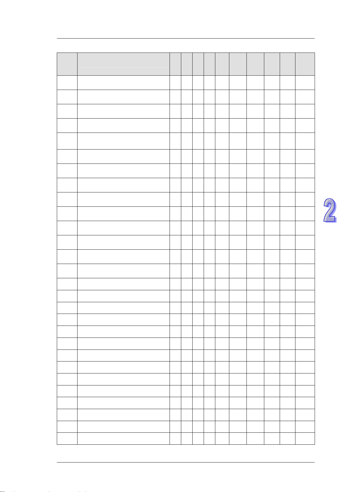
Special
M
Function
ES2
SS2 SA2 SX2
EX2
OFF
Ø
ON
2. Programming Concepts
STOP
RUN
Ø
RUN
Ø
STOP
Attrib.
Latch
-ed
Default
M1378*
M1379*
M1380*
M1381*
M1382*
M1383*
M1384*
M1385*
M1386*
M1387*
M1388*
M1389*
M1390*
M1391*
M1392* Slave ID#1 linking error
Indicate Slave ID#3 data interchange
status on PLC LINK
Indicate Slave ID#4 data interchange
status on PLC LINK
Indicate Slave ID#5 data interchange
status on PLC LINK
Indicate Slave ID#6 data interchange
status on PLC LINK
Indicate Slave ID#7 data interchange
status on PLC LINK
Indicate Slave ID#8 data interchange
status on PLC LINK
Indicate Slave ID#9 data interchange
status on PLC LINK
Indicate Slave ID#10 data interchange
status on PLC LINK
Indicate Slave ID#11 data interchange
status on PLC LINK
Indicate Slave ID#12 data interchange
status on PLC LINK
Indicate Slave ID#13 data interchange
status on PLC LINK
Indicate Slave ID#14 data interchange
status on PLC LINK
Indicate Slave ID#15 data interchange
status on PLC LINK
Indicate Slave ID#16 data interchange
status on PLC LINK
○ ○ ○ ○
○ ○ ○ ○
○ ○ ○ ○
○ ○ ○ ○
○ ○ ○ ○
○ ○ ○ ○
○ ○ ○ ○
○ ○ ○ ○
○ ○ ○ ○
○ ○ ○ ○
○ ○ ○ ○
○ ○ ○ ○
○ ○ ○ ○
○ ○ ○ ○
○ ○ ○ ○
OFF - - R NO OFF
OFF - - R NO OFF
OFF - - R NO OFF
OFF - - R NO OFF
OFF - - R NO OFF
OFF - - R NO OFF
OFF - - R NO OFF
OFF - - R NO OFF
OFF - - R NO OFF
OFF - - R NO OFF
OFF - - R NO OFF
OFF - - R NO OFF
OFF - - R NO OFF
OFF - - R NO OFF
OFF - - R NO OFF
M1393* Slave ID#2 linking error
M1394* Slave ID#3 linking error
M1395* Slave ID#4 linking error
M1396* Slave ID#5 linking error
M1397* Slave ID#6 linking error
M1398* Slave ID#7 linking error
M1399* Slave ID#8 linking error
M1400* Slave ID#9 linking error
M1401* Slave ID#10 linking error
M1402* Slave ID#11 linking error
M1403* Slave ID#12 linking error
M1404* Slave ID#13 linking error
M1405* Slave ID#14 linking error
○ ○ ○ ○
○ ○ ○ ○
○ ○ ○ ○
○ ○ ○ ○
○ ○ ○ ○
○ ○ ○ ○
○ ○ ○ ○
○ ○ ○ ○
○ ○ ○ ○
○ ○ ○ ○
○ ○ ○ ○
○ ○ ○ ○
○ ○ ○ ○
OFF - - R NO OFF
OFF - - R NO OFF
OFF - - R NO OFF
OFF - - R NO OFF
OFF - - R NO OFF
OFF - - R NO OFF
OFF - - R NO OFF
OFF - - R NO OFF
OFF - - R NO OFF
OFF - - R NO OFF
OFF - - R NO OFF
OFF - - R NO OFF
OFF - - R NO OFF
2-27
Page 60

DVP-ES2/EX2/SS2/SA2/SX2/SE Operation Manual - Programming
OFF
Special
M
Function
ES2
SS2 SA2 SX2
EX2
Ø
ON
STOP
Ø
RUN
STOP
RUN
Ø
Attrib.
Latch
-ed
Default
M1406* Slave ID#15 linking error
M1407* Slave ID#16 linking error
M1408*
M1409*
M1410*
M1411*
M1412*
M1413*
M1414*
M1415*
M1416*
M1417*
M1418*
M1419*
M1420*
M1421*
M1422*
M1423*
M1424*
M1425*
M1426*
M1427*
M1428*
M1429*
M1430*
M1431*
M1432*
M1433*
M1434*
M1435*
M1436*
Indicate that reading from Slave ID#1 is
completed
Indicate that reading from Slave ID#2 is
completed
Indicate that reading from Slave ID#3 is
completed
Indicate that reading from Slave ID#4 is
completed
Indicate that reading from Slave ID#5 is
completed
Indicate that reading from Slave ID#6 is
completed
Indicate that reading from Slave ID#7 is
completed
Indicate that reading from Slave ID#8 is
completed
Indicate that reading from Slave ID#9 is
completed
Indicate that reading from Slave ID#10 is
completed
Indicate that reading from Slave ID#11 is
completed
Indicate that reading from Slave ID#12 is
completed
Indicate that reading from Slave ID#13 is
completed
Indicate that reading from Slave ID#14 is
completed
Indicate that reading from Slave ID#15 is
completed
Indicate that reading from Slave ID#16 is
completed
Indicate that writing to Slave ID#1 is
completed
Indicate that writing to Slave ID#2 is
completed
Indicate that writing to Slave ID#3 is
completed
Indicate that writing to Slave ID#4 is
completed
Indicate that writing to Slave ID#5 is
completed
Indicate that writing to Slave ID#6 is
completed
Indicate that writing to Slave ID#7 is
completed
Indicate that writing to Slave ID#8 is
completed
Indicate that writing to Slave ID#9 is
completed
Indicate that writing to Slave ID#10 is
completed
Indicate that writing to Slave ID#11 is
completed
Indicate that writing to Slave ID#12 is
completed
Indicate that writing to Slave ID#13 is
completed
○ ○ ○ ○
○ ○ ○ ○
○ ○ ○ ○
○ ○ ○ ○
○ ○ ○ ○
○ ○ ○ ○
○ ○ ○ ○
○ ○ ○ ○
○ ○ ○ ○
○ ○ ○ ○
○ ○ ○ ○
○ ○ ○ ○
○ ○ ○ ○
○ ○ ○ ○
○ ○ ○ ○
○ ○ ○ ○
○ ○ ○ ○
○ ○ ○ ○
○ ○ ○ ○
○ ○ ○ ○
○ ○ ○ ○
○ ○ ○ ○
○ ○ ○ ○
○ ○ ○ ○
○ ○ ○ ○
○ ○ ○ ○
○ ○ ○ ○
○ ○ ○ ○
○ ○ ○ ○
○ ○ ○ ○
○ ○ ○ ○
OFF - - R NO OFF
OFF - - R NO OFF
OFF - - R NO OFF
OFF - - R NO OFF
OFF - - R NO OFF
OFF - - R NO OFF
OFF - - R NO OFF
OFF - - R NO OFF
OFF - - R NO OFF
OFF - - R NO OFF
OFF - - R NO OFF
OFF - - R NO OFF
OFF - - R NO OFF
OFF - - R NO OFF
OFF - - R NO OFF
OFF - - R NO OFF
OFF - - R NO OFF
OFF - - R NO OFF
OFF - - R NO OFF
OFF - - R NO OFF
OFF - - R NO OFF
OFF - - R NO OFF
OFF - - R NO OFF
OFF - - R NO OFF
OFF - - R NO OFF
OFF - - R NO OFF
OFF - - R NO OFF
OFF - - R NO OFF
OFF - - R NO OFF
OFF - - R NO OFF
OFF - - R NO OFF
2-28
Page 61

2. Programming Concepts
OFF
Special
M
M1437*
M1438* OFF - - R NO OFF
M1439*
M1524
M1525 OFF - - R/W NO OFF
M1534
Indicate that writing to Slave ID#14 is
completed
Indicate that writing to Slave ID#15 is
completed
Indicate that writing to Slave ID#16 is
completed
Auto-reset Y2 when high speed pulse
output is completed
Auto-reset Y3 when high speed pulse
output is completed
Enable ramp-down time setting on Y0.
Has to be used with D1348.
Function
ES2
SS2 SA2 SX2
EX2
○ ○ ○ ○
○ ○ ○ ○
○ ○ ○ ○
○ ○ ○ ○
○ ○ ○ ○
○ ○ ○ ○
STOP
Ø
ON
RUN
OFF - - R NO OFF
OFF - - R NO OFF
OFF - - R/W NO OFF
OFF - - R/W NO OFF
Ø
RUN
Ø
STOP
Attrib.
Latch
-ed
Default
M1535
M1538 Indicate pause status of Y0 OFF OFF - R/W NO OFF
M1539 Indicate pause status of Y1 OFF OFF - R/W NO OFF
M1540 Indicate pause status of Y2 OFF OFF - R/W NO OFF
M1541 Indicate pause status of Y3 OFF OFF - R/W NO OFF
Enable ramp-down time setting on Y2.
Has to be used with D1349.
○ ○ ○ ○
○ ○ ○ ○
○ ○ ○ ○
○ ○ ○ ○
○ ○ ○ ○
OFF - - R/W NO OFF
2-29
Page 62

DVP-ES2/EX2/SS2/SA2/SX2/SE Operation Manual - Programming
2.9 S Relay
Initial step relay
Starting instruction in Sequential Function Chart (SFC).
S0~S9, total 10 points.
Zero return step relay
Returns to zero point when using IST instruction in program. Zero
return step relays not used for IST instruction can be used as
general step relays.
S10~S19, total 10 ponits.
Latched step relay
In sequential function chart (SFC), latched step relay will be saved
when power loss after running. The state of power on after power
loss will be the same as the sate before power loss.
S20 ~ S127, total 108 points.
General purpose step relay
General relays in sequential function chart (SFC). They will be
cleared when power loss after running.
S128 ~ S911, total 784 points.
Alarm step relay
Used with alarm driving instruction API 46 ANS as an alarm
contact for recording the alarm messages or eliminating external
malfunctions.
S912 ~ S1023, total 112 points.
2.10 T (Timer)
The units of the timer are 1ms, 10ms and 100ms and the counting method is counting up. When
the present value in the timer equals the set value, the associated output coil will be ON. The set
value should be a K value in decimal and can be specified by the content of data register D.
The actual set time in the timer = timer resolution× set value
Ex: If set value is K200 and timer resolution is 10ms, the actual set time in timer will be 10ms*200 =
2000ms = 2 sec.
General Timer
The timer executes once when the program reaches END instruction. When TMR instruction is
executed, the timer coil will be ON when the current value reaches its preset value.
When X0 = ON, TMR instruction is driven. When current value achieves K100, the assocailte timer
contact T0 is ON to drive Y0. If X0 = OFFor the power is off, the current value in T0 will be cleared
as 0 and output Y0 driven by contact T0 will be OFF.
X0
TMR T0 K100
T0
2-30
X0
T0
Y0
Y0
present
value
10 sec
K100
Page 63

2. Programming Concepts
Accumulative Timer
The timer executes once when the program reaches END instruction. When TMR instruction is
executed, the timer coil will be ON when the current value reaches its preset value. For
accumulative timers, current value will not be cleared when timing is interrupted.
Timer T250 will be driven when X0 = ON. When X0 = OFFor the power is off, timer T250 will pause
and retain the current value. When X0 is ON again, T250 resumes timing from where it was paused.
X0
T250 K100
T2
T1+T2=10sec
K100
X0
T250
TMR
T250
Y0
T1
present
value
Y0
Timers for Subroutines and Interrupts
Timers for subroutines and interrupts count once when END instruction is met. The associated
output coils will be ON if the set value is achieved when End instruction executes. T184~T199 are
the only timers that can be used in subroutines or interrupts. Generals timers used in subroutines
and interrupts will not work if the subroutines or interrupts are not executing.
2.11 C (Counter)
Counters will increment their present count value when input signals are triggered from OFFON.
32 bits counters
Type General General High speed
Counters C0~C199 C200~C231(C232)
Count
direction
Range 0~32,767 -2,147,483,648~+2,147,483,647 0~2,147,483,647
Preset
value
register
Output
operation
16 bits
counters
C232(C233)~C242,
C245~C254
C243, C244
Count up Count up/down Count up
Constant K or
data register
Constant K or data register D (Dword)
D (Word)
Counter will keep on
Counter will
stop when
preset value
reached
Counter will keep on counting when preset
value reached. The count value will become
-2,147,483,648 if one more count is added
to +2,147,483,647
counting when preset
value is reached. The
count value will
become 0 if one more
count is added to
+2,147,483,647
2-31
Page 64

DVP-ES2/EX2/SS2/SA2/SX2/SE Operation Manual - Programming
32 bits counters
Output
contact
function
16 bits
counters
Ouptut Coil
will be ON
when counter
reaches
preset value.
Output coil is ON when counter reaches or
is above preset value.
Output coil is OFF when counter is below
preset value.
Associated devices
are activated
High speed
conparison
- -
immediately when
preset value is
reached, i.e.
independant of scan
time.
Reset
action
The present value will reset to 0 when RST instruction is executed, output coil will
be OFF.
Example:
LD X0
RST C0
LD X1
CNT C0 K5
LD C0
OUT Y0
When X0 = ON, RST instruction resets
C0. Every time When X1 is driven, C0 will
count up (add 1).
When C0 reaches the preset value K5,
output coil Y0 will be ON and C0 will stop
counting and ignore the signals from input
X1.
X0
X1
C0
X0
X1
C0
present
value
Output coil is ON
when counter
reaches or is above
preset value
C0RST
C0 K 5CNT
Y0
5
4
3
2
1
0
settings
0
2-32
Contacts Y0, C0
Page 65

2. Programming Concepts
M relays M1200~M1254 are used to set the up/down counting direction for C200~C254
respectively. Setting the corresponding M relay ON will set the counter to count down.
Example:
LD X10
OUT M1200
LD X11
RST C200
LD X12
CNT C200 K-5
LD C200
OUT Y0
a) X10 drives M1200 to
determine counting direction
(up / down) of C200
b) When X11 goes from OFF to
ON, RST instsruction will be
executed and the PV (present
value) in C200 will be cleared
and contact C200 is OFF.
c) When X12 goes from Off to
On, PV of C200 will count up
X10
X11
X12
C200
Accumulatively
X10
X11
increasing
M1200
Y0
C200RST
C200 K-5DCNT
Progressively
decreasing
Accumulatively
increasing
(plus 1) or count down (minus
1).
d) When PV in C200 changes
from K-6 to K-5, the contact
C200 will be energized. When
PV in C200 changes from K-5
to K-6, the contact of C200
will be reset.
e) If MOV instruction is applied
through WPLSoft or HPP to
designate a value bigger than
SV to the PV register of C0,
next time when X1 goes from
OFF to ON, the contact C0
will be ON and PV of C0 will
equal SV.
X12
PV in
C200
Contacts
Y0, C0
454
3
2
1
0
When the output contact
was On.
3
2
1
0
-1
-2
-3
-4
-5
-6
-6
-7
-7
-8
0
-3
-4
-5
2-33
Page 66

DVP-ES2/EX2/SS2/SA2/SX2/SE Operation Manual - Programming
2.12 High-speed Counters
There are two types of high speed counters provided including Software High Speed Counter
(SHSC) and Hardware High Speed Counter (HHSC). The same Input point (X) can be designated
with only one high speed counter. Double designation on the same input or the same counter will
result in syntax error when executing DCNT instruction.
Applicable Software High Speed Counters:
C
X
X0
X1 U/D
X2 U/D B
X3 U/D
X4 U/D A
X5 U/D B
X6 U/D A
X7 U/D B
R/F M1270 M1271 M1272 M1273 M1274 M1275 M1276 M1277 - - -
U/D M1235 M1236 M1237 M1238 M1239 M1240 M1241 M1242 - - -
C235 C236 C237 C238 C239 C240 C241 C242 C232 C233 C234
U/D
1-phase input 2 phase 2 input
A
U: Count up D: Count down A: Phase A input B: Phase B input
Note:
1. U/D (Count up/Count down) can be specified by special M. OFF = count up; ON = count down.
2. R/F (Rising edge trigger/ Falling edge trigger) can also be specified by special M. OFF =
Rising; ON = Falling.
3. SHSC supports max 10kHz input pulse on single point. Max 8 counters are applicable in the
same time.
4. SS2 model does not support 2-phase 2-input conuting by (X0,X2) (C232).
5. For 2-phase 2-input conuting, (X4, X5) (C233) and (X6, X7) (C234), max 5kHz. (X0,X2)
(C232), max 15kHz.
6. 2-phase 2-input counting supports double and quadruple frequency, which is selected in
D1022 as the table in next page
2-34
Page 67

Applicable Hardware High Speed Counters:
2. Programming Concepts
C
1-phase
1-phase 2-input 2-phase 2-input
X
input
C243 C244 C245 C246 C247 C248 C249 C250 C251 C252 C253 C254
X0 U U/D U/D U U A A
X1 R Dir Dir D D B B
X2 U U/D U/D A A
X3 R Dir Dir B B
X4 R R R
X5 R R
U: Count up A: Phase A input Dir: Directoin signal input
D: Count down B: Phase B input R: Reset signal input
Note:
1. The max frequency of the 1-phase input counters X0 (C243) and X2(C244) is 100kHz on
ES2/EX2/SA2/SX2 model and 20kHz on SS2 model.
2. The max frequency of the 1-phase 2-input counters (X0, X1)(C245, C246) and (X2, X3)(C249,
C250) is 100kHz on ES2/EX2/SA2/SX2 model and 20kHz on SS2 model.
3. The max frequency of the 1-phase 2-input counters (X0, X1)(C247, C248) is 10kHz on
ES2/EX2/SS2/SX2 model and 100kHz on 32ES211T and SA2 model..
4. The max frequency of the 2-phase 2-input counter (X0, X1)(C251, C252) is 5kHz on ES2/EX2
model, 10kHz on SS2/SX2 model and 50kHz on 32ES211T and SA2 model.
5. The max frequency of the 2-phase 2-input counter (X2, X3)(C253, C254) is 5kHz on
ES2/EX2/SA2 model, 10 kHz on SS2/SX2 model and 50kHz on 32ES211T.
6. 2-phase 2-input counting supports double and 4 times frequency, which is selected in D1022
as the table in next page. Please refer to the below table for detailed counting wave form.
D1022 Counting mode
A
A
B
B
K2
(Double Frequency)
dow
dow
n
n
t
t
n
n
u
u
o
o
c
c
p
p
u
u
c
c
o
o
un
un
t
t
A
A
B
B
K4 or other value
(Quadruple frequency)
d
d
o
o
w
w
n
n
(Default)
t
t
n
n
u
u
o
o
c
c
p
p
u
u
c
c
o
o
u
u
n
n
t
t
2-35
Page 68

DVP-ES2/EX2/SS2/SA2/SX2/SE Operation Manual - Programming
7. C243 and C244 support count-up mode only and occupy the associate input points X1 and
X3 as reset (“R”) function. If users do not need to apply reset function, set ON the associated
special M relays (M1243 and M1244) to disable the reset function.
8. “Dir” refers to direction control function. OFF indicates counting up; ON indicates counting
down.
9. When X1, X3, X4 and X5 is applied for reset function and associated external interrupts are
disabled, users can define the reset function as Rising/Falling-edge triggered by special M
relays
Reset Function X1 X3 X4 X5
R/F M1271 M1273 M1274 M1275
10. When X1, X3, X4 and X5 is applied for reset function and external interrupts are applied, the
interrupt instructions have the priority in using the input points. In addition, PLC will move the
current data in the counters to the associated data registers below then reset the counters.
Special D D1241, D1240 D1243, D1242
Counter C243 C246 C248 C252 C244 C250 C254
External Interrupt
X1
(I100/I101)
X4(I400/I401)
X3
(I300/I301)
X5(I500/I501)
Example:
EI
I101
M1000
M1000
DCNT
DMOV
C243 K100
FEND
D1240 D0
IRET
END
When C243 is counting and external interrupt is triggerred from X1(I101), counted value in C243
will be move to (D1241, D1240) immediately then C243 is reset. After this interrupt I101 executes.
1-phase 1 input high-speed counter:
Example:
LD X20
RST C235
LD X21
OUT M1235
LD X22
DCNT C235 K5
LD C235
OUT Y0
X20
C235RST
X21
M1235
X22
C235 K5DCNT
C235
Y0
2-36
Page 69

2. Programming Concepts
1. X21 drives M1235 to determine counting direction (Up/Down) of C235.
2. When X20 = ON, RST instsruction executes and the current value in C235 will be cleared.
Contact C235 will be OFF
3. When X22 = ON, C235 receives signals from X0 and counter will count up (+1) or count
down (-1).
4. When counter C235 reaches K5, contact C235 will be ON. If there is still input signal inp ut
for X0, it will keep on counting.
counting down
X21,M1243 contact
X20
X22
X0
counting up
C243
present
value
3
1
0
Y0, C243 contact
1-phase 2 inputs high-speed counter:
Example:
LD X20
RST C247
LD X21
DCNT C247 K5
LD C247
OUT Y0
7
6
5
4
3
2
6
5
4
X20
C247RST
X21
C247 K 5DCNT
C247
Y0
1. When X20 is ON, RST instsruction executes and the current value in C247 will be cleared.
Contact C247 will be OFF.
2. When X21=ON, C247 receives count signals from X0 and counter counts up (+1), or
C247 receives count signal from X1 and counter count s down (-1)
3. When C247 reaches K5, contact C247 will be ON. If there is still input signal from X0 or
X1, C247 will keep on counting
2-37
Page 70

DVP-ES2/EX2/SS2/SA2/SX2/SE Operation Manual - Programming
X20
X21
X0
count up
X1
count down
C247
present
value
3
0
Y0, C 2 47 contact
5
4
3
2
1
7
6
6
AB-phase input high-speed counter:
5
4
Example:
LD M1002
MOV K2 D1022
LD X20
RST C251
LD X21
DCNT C251 K5
LD C251
M1002
K2 D1 022MOV
X20
C251RST
X21
C251 K 5DCNT
C251
Y0
OUT Y0
1. When X20 is ON, RST instsruction executes and the current value in C251 will be cleared.
Contact C251 will be OFF.
2. When X21 is ON, C251 receives A phase counting signal of X0 input terminal and B
phase counting signal of X1 input terminal and executes count up or count down
3. When counter C251 reaches K5, contact C251 will be ON. If there is still input signal from
X0 or X1, C251 will keep on counting
4. Counting mode can be specified as double frequency or 4-times frequency by D1022.
Default: quadruple frequency.
2-38
Page 71

2. Programming Concepts
X20
X21
A-phase X0
B-phase X1
6
C251 present value
3
5
4
3
2
1
0
Counti ng up
5
4
3
Cou nt i ng do w n
2
1
0
Y0, C251 contact
2.13 Special Data Register
The types and functions of special registers (special D) are listed in the table below. Care should
be taken that some registers of the same No. may bear different meanings in different series MPUs.
Special M and special D marked with “*” will be further illustrated in 2.13. Columns marked with “R”
refers to “read only”, “R/W” refers to “read and write”, “-“ refers to the status remains unchanged
and “#” refers to that system will set it up according to the status of the PLC. For detailed
explanation please also refer to 2.13 in this chapter.
OFF
STOP
Special
D
D1000* 200 - - R/W NO 200
D1001 - - - R NO #
D1002* - - - R NO #
D1003 # - - R YES 15872
D1004* 0 0 - R NO 0
SV of program scan ning WDT (Unit: 1ms)
Displaying the firmware version of DVP-PLC
(initial factory setting)
Program capacity
Sum of program memory (sum of the PLC internal
program memory.
Syntax check error code
Content
ES2
EX2SS2SA2SX2
○ ○ ○ ○
○ ○ ○ ○
○ ○ ○ ○
○ ○ ○ ○
○ ○ ○ ○
Ø
ON
Ø
RUN
RUN
Ø
STOP
Attrib.
Latch
-ed
Default
D1008* 0 - - R NO 0
D1009 - - - R YES 0
D1015* 0 - - R/W NO 0
D1018*
D1019*
D1020* 10 - - R/W NO 10
D1022
Step address when WDT is ON
Number of LV (Low voltage) signal occurrence
Current scan time (Unit: 0.1ms)
Minimum scan time (Unit: 0.1ms)
Maximum scan time (Unit: 0.1ms)
Value of accumulative high-speed timer
(0~32,767, unit: 0.1ms)
πPI (Low byte)
πPI(High byte)
X0~X7 input filter (unit: ms) 0~20ms adjustable
Counting mode selection (Double frequency/ 4
times frequency) for AB phase counter (From X0,
X1 input)
○ ○ ○ ○
○ ○ ○ ○
○ ○ ○ ○
○ ○ ○ ○
○ ○ ○ ○
○ ○ ○ ○
○ ○ ○ ○
○ ○ ○ ○
○ ○ ○ ○
○ ○ ○ ○
# # # D1010* R NO 0
# # # D1011* R NO 0
# # # D1012* R NO 0
H’
H’
H’
0FDB
0FDB
H’
4049
H’
4049
4 - - R/W NO 4
0FDB
H’
4049
R/W NO
R/W NO
H’
0FDB
H’
4049
2-39
Page 72

DVP-ES2/EX2/SS2/SA2/SX2/SE Operation Manual - Programming
OFF
Special
D
D1023*
D1025*
D1026*
D1027*
D1028
D1029
D1030
D1031
Content
Register for Storing detected pulse width (unit:
0.1ms)
Code for communication request error
Pulse number for masking Y0 when M1156 = ON
(Low word)
Pulse number for masking Y0 when M1156 = ON
(High word)
Index register E0
Index register F0
PV of Y0 pulse output (Low word)
PV of Y0 pulse output (High word)
ES2
EX2SS2SA2SX2
○ ○ ○ ○
○ ○ ○ ○
○ ○ ○ ○
○ ○ ○ ○
○ ○ ○ ○
○ ○ ○ ○
○ ○ ○ ○
○ ○ ○ ○
STOP
Ø
Ø
ON
RUN
0 - - R/W NO 0
0 - - R NO 0
0 0 - R/W NO 0
0 0 - R/W NO 0
0 - - R/W NO 0
0 - - R/W NO 0
- - - R/W YES 0
- - - R/W YES 0
RUN
Ø
STOP
Attrib.
Latch
-ed
Default
D1032
D1033
D1036*
D1037*
D1038
D1039*
D1040
D1041
D1042
D1043
D1044
D1045
D1046
D1047
PV of Y1 pulse output (Low word)
PV of Y1 pulse output (High word)
COM1 (RS-232) communication protocol
Register for setting 8-sets SPD function (has to be
used with M1037)
1. Delay time setting for data response when PLC
is SLAVE in COM2 / COM3 RS-485
communication. Range: 0 ~ 10,000 (unit: 0.1ms).
2. By using PLC LINK in COM2 (RS-485), D1038
can be set to send next communication data with
delay. Range: 0 ~ 10,000 (Unit: one scan cycle)
Fixed scan time (ms)
No. of the 1st step point which is ON.
No. of the 2nd step point which is ON
No. of the 3rd step point which is ON.
No. of the 4th step point which is ON
No. of the 5th step point which is ON.
No. of the 6th step point which is ON
No. of the 7th step point which is ON.
No. of the 8th step point which is ON
○ ○ ○ ○
○ ○ ○ ○
○ ○ ○ ○
○ ○ ○ ○
○ ○ ○ ○
○ ○ ○ ○
○ ○ ○ ○
○ ○ ○ ○
○ ○ ○ ○
○ ○ ○ ○
○ ○ ○ ○
○ ○ ○ ○
○ ○ ○ ○
○ ○ ○ ○
0 - - R/W NO 0
0 - - R/W NO 0
H’86 - - R/W NO H’86
0 - - R/W NO 0
- - - R/W NO 0
0 - - R/W NO 0
0 - - R NO 0
0 - - R NO 0
0 - - R NO 0
0 - - R NO 0
0 - - R NO 0
0 - - R NO 0
0 - - R NO 0
0 - - R NO 0
D1049
D1050
↓
D1055
D1062*
D1067*
D1068*
2-40
No. of alarm which is ON
Converted data for Modbus communication data
processing. PLC automatically converts the ASCII
data in D1070~D1085 into Hex data and stores
the 16-bit Hex data into D1050~D1055
Average number of times an analog signal is input
to the EX2/SX2 series PLC
The default value is K10 for EX2 version 2.6 and
version 2.8.
Error code for program execution error
Address of program execution error
○ ○ ○ ○
○ ○ ○ ○
○ ╳ ╳ ○
○ ○ ○ ○
○ ○ ○ ○
0 - - R NO 0
0 - - R NO 0
2 - - R/W YES 2
0 0 - R NO 0
0 - - R NO 0
Page 73

Special
D
D1070
↓
D1085
D1086
D1087
D1089
↓
D1099
D1109*
D1110*
D1111*
D1112*
D1113*
D1114*
D1115*
D1116*
D1117*
D1118*
D1120*
D1121*
D1122
D1123
Content
Feedback data (ASCII) of Modbus
communication. When PLC’s RS-485
communication instruction receives feedback
signals, the data will be saved in the registers
D1070~D1085. Usres can check the received
data in these registers.
High word of the password in DVP-PCC01
(displayed in hex according to its ASCII codes)
Low word of the password in DVP-PCC01
(displayed in hex according to its ASCII codes)
Sent data of Modbus communication.
When PLC’s RS-485 communication instruction
sends out data, the data will be stored in
D1089~D1099. Users can check the sent data in
these registers.
COM3 (RS-485) Communication protocol
Average value of EX2/SX2 analog input channel 0
(AD 0) When average times in D1062 is set to 1,
D1110 indicates present value.
Average value of EX2/SX2 analog input channel 1
(AD 1) When average times in D1062 is set to 1,
D1111 indicates present value
Average value of EX2/SX2 analog input channel 2
(AD 2) Whenaverage times in D1062 is set to 1,
D1112 indicates present value
Average value of 20EX2/SX2 analog input
channel 3 (AD 3) Whenaverage times in D1062 is
set to 1, D1113 indicates present value
Displaying the status of the analog input channel
of 30EX2
Enable/disable 20EX2/SX2 AD channels
(0: enable (default) / 1: disable)
bit0~bit3 sets AD0~AD3.
P.S. 30EX2 does not support this function.
20EX2/SX2 analog input/output mode setting
30EX2 analog input/output mode setting
Output value of analog output channel 0 (DA 0) of
EX2/SX2
Output value of analog output channel 1 (DA 0) of
20EX2/SX2
P.S. 30EX2 does not support this function.
EX2/SX2 sampling time of analog/digital
converstion. Default: 2. Unit: 1ms. Sampling time
will be regarded as 2ms if D1118≦2
COM2 (RS-485) communication protocol
COM1(RS-232) and COM2(RS-485) PLC
communication address
COM2(RS-485) Residual number of words of
transmitting data
COM2(RS-485) Residual number of words of the
receiving data
ES2
EX2SS2SA2SX2
○ ○ ○ ○
○ ○ ○ ○
○ ○ ○ ○
○ ○ ○ ○
○ ╳ ○ ○
○ ╳ ╳ ○
○ ╳ ╳ ○
○ ╳ ╳ ○
○ ╳ ╳ ○
○ ╳ ╳ ╳
○ ╳ ╳ ○
○ ╳ ╳ ○
○ ╳ ╳ ╳
○ ╳ ╳ ○
○ ╳ ╳ ○
○ ╳ ╳ ○
○ ○ ○ ○
○ ○ ○ ○
○ ○ ○ ○
○ ○ ○ ○
2. Programming Concepts
OFF
STOP
Ø
RUN
RUN
Ø
STOP
Ø
ON
0 - - R NO 0
0 - - R/W NO 0
0 - - R/W NO 0
0 - - R NO 0
H’86 - - R/W NO H’86
0 - - R NO 0
0 - - R NO 0
0 - - R NO 0
0 - - R NO 0
0 - - R NO 0
0 - - R/W YES 0
0 0 0 R/W YES 0
- - - R/W YES H’FFFF
0 0 0 R/W NO 0
0 0 0 R/W NO 0
2 - - R/W YES 2
H’86 - - R/W NO H’86
- - - R/W Yes 1
0 0 - R NO 0
0 0 - R NO 0
Attrib.
Latch
-ed
Default
2-41
Page 74

DVP-ES2/EX2/SS2/SA2/SX2/SE Operation Manual - Programming
OFF
Special
D
D1124
D1125
D1126
D1127
D1128
D1129
D1130
D1131
D1132
D1133
D1134
D1135*
D1136*
D1137*
Content
COM2(RS-485) Definition of start character (STX)
COM2(RS-485) Definition of first ending character
(ETX1)
COM2(RS-485) Definition of second ending
character (ETX2)
Number of pulses for ramp-up operation of
positioning instruction (Low word)
Number of pulses for ramp-up operation of
positioning instruction (High word)
COM2 (RS-485) Communication time-out setting
(ms)
COM2 (RS-485) Error code returning from
Modbus
Input/output percentage value of CH0(Y0,Y1)
close loop control
Input/output percentage value of CH1(Y2,Y3)
close loop control
Number of pulses for ramp-down operation of
positioning instruction (Low word)
Number of pulses for ramp-down operation of
positioning instruction (High word)
Pulse number for masking Y2 when M1158 = ON
(Low word)
Pulse number for masking Y2 when M1158 = ON
(High word)
Address where incorrect use of operand occurs
ES2
EX2SS2SA2SX2
○ ○ ○ ○
○ ○ ○ ○
○ ○ ○ ○
○ ○ ○ ○
○ ○ ○ ○
○ ○ ○ ○
○ ○ ○ ○
○ ○ ○ ○
○ ○ ○ ○
○ ○ ○ ○
○ ○ ○ ○
○ ○ ○ ○
○ ○ ○ ○
○ ○ ○ ○
STOP
Ø
Ø
ON
RUN
H’3A - - R/W NO H’3A
H’0D - - R/W NO H’0D
H’0A - - R/W NO H’0A
0 - - R/W NO 0
0 - - R/W NO 0
0 - - R NO 0
100 - - R/W NO 100
100 - - R/W NO 100
0 - - R NO 0
0 - - R NO 0
0 0 - R/W NO 0
0 0 - R/W NO 0
0 0 - R NO 0
RUN
Ø
STOP
Attrib.
Latch
-ed
Default
D1140*
D1142*
D1143*
D1145*
D1167
D1168
D1169
D1178
D1179
D1182
D1183
D1184
D1185
Number of I/O modules (max. 8)
Number of input points (X) on DIO modules
Number of output points (Y) on DIO modules
Number of the connected let-side modules
The specific end word to be detected for RS
instruction to execute an interruption request
(I140) on COM1 (RS-232).
The specific end word to be detected for RS
instruction to execute an interruption request
(I150) on COM2 (RS-485)
The specific end word to be detected for RS
instruction to execute an interruption request
(I160) on COM3 (RS-485)
VR0 value
VR1 value
Index register E1
Index register F1
Index register E2
Index register F2
○ ○ ○ ○
○ ○ ○ ○
○ ○ ○ ○
╳ ╳ ○ ○
○ ○ ○ ○
○ ○ ○ ○
○ ╳ ○ ╳
╳ ╳ ○ ○
╳ ╳ ○ ○
○ ○ ○ ○
○ ○ ○ ○
○ ○ ○ ○
○ ○ ○ ○
0 - - R NO 0
0 - - R NO 0
0 - - R NO 0
0 - - R NO 0
0 - - R/W NO 0
0 - - R/W NO 0
0 - - R/W NO 0
0 - - R NO 0
0 - - R NO 0
0 - - R/W NO 0
0 - - R/W NO 0
0 - - R/W NO 0
0 - - R/W NO 0
D1186
2-42
Index register E3
○ ○ ○ ○
0 - - R/W NO 0
Page 75
Special
D
D1187
Index register F3
Content
ES2
EX2SS2SA2SX2
○ ○ ○ ○
2. Programming Concepts
OFF
STOP
Ø
RUN
RUN
Ø
STOP
Ø
ON
0 - - R/W NO 0
Attrib.
Latch
-ed
Default
D1188
D1189
D1190
D1191
D1192
D1193
D1194
D1195
D1220
D1221
D1232*
D1233*
D1234*
D1235*
D1240*
D1241*
D1242*
D1243*
D1244
D1245
D1249
D1250
D1252
Index register E4
Index register F4
Index register E5
Index register F5
Index register E6
Index register F6
Index register E7
Index register F7
Pulse output mode setting of CH0 (Y0, Y1)
Pulse output mode setting of CH1 (Y2, Y3)
Number of output pulses for CH0 (Y0, Y1) rampdown stop when mark sensor receives signals.
(Low word).
Number of output pulses for CH0 (Y0, Y1) rampdown stop when mark sensor receives signals.
(High word).
Number of output pulses for CH1 (Y2, Y3) rampdown stop when mark sensor receives signals.
(Low word).
Number of output pulses for CH2 (Y2, Y3) rampdown stop when mark sensor receives signals.
(High word).
When interupt I400/I401/I100/I101 occurs,
D1240 stores the low word of high-speed counter.
When interupt I400/I401/I100/I101 occurs,
D1241 stores the high Word of high-speed
counter.
When interupt I500/I501/I300/I301 occurs,
D1242 stores the low Wordof high-speed counter.
When interupt I500/I501/I300/I301 occurs, D1243
stores the high Word of high-speed counter.
Idle time (pulse number) setting of CH0 (Y0, Y1)
The function is disabled if set value≦0.
Idle time (pulse number) setting of CH1 (Y2, Y3)
The function is disabled if set value≦0.
Set value for COM1 (RS-232) data receiving timeout (Unit: 1ms, min. 50ms, value smaller than
50ms will be regarded as 50ms) (only applicable
for MODRW/RS instruction) In RS instruction, no
time-out setting if “0” is specified.
COM1 (RS-232) communication error code (only
applicable for MODRW/RS instruction)
Set value for COM3 (RS-485) data receiving timeout (Unit: 1ms, min. 50ms, value smaller than
50ms will be regarded as 50ms) (only applicable
for MODRW/RS instruction) In RS instruction, no
time-out setting if “0” is specified
○ ○ ○ ○
○ ○ ○ ○
○ ○ ○ ○
○ ○ ○ ○
○ ○ ○ ○
○ ○ ○ ○
○ ○ ○ ○
○ ○ ○ ○
○ ○ ○ ○
○ ○ ○ ○
○ ○ ○ ○
○ ○ ○ ○
○ ○ ○ ○
○ ○ ○ ○
○ ○ ○ ○
○ ○ ○ ○
○ ○ ○ ○
○ ○ ○ ○
○ ○ ○ ○
○ ○ ○ ○
○ ○ ○ ○
○ ○ ○ ○
○ ╳ ○ ╳
0 - - R/W NO 0
0 - - R/W NO 0
0 - - R/W NO 0
0 - - R/W NO 0
0 - - R/W NO 0
0 - - R/W NO 0
0 - - R/W NO 0
0 - - R/W NO 0
0
- -
0
- -
0 0 -- R/W NO 0
0 0 -- R/W NO 0
0 0 -- R/W NO 0
0 0 -- R/W NO 0
0 0 - R
0 0 - R
0 0 - R
0 0 - R
0 - - R/W NO 0
0 - - R/W
0 - - R/W NO 0
0 - - R/W
50 - - R/W NO50
R/W
R/W
NO
NO
NO
NO
NO
NO
NO
NO
0
0
0
0
0
0
0
0
2-43
Page 76

DVP-ES2/EX2/SS2/SA2/SX2/SE Operation Manual - Programming
OFF
Special
D
D1253
Content
COM3 (RS-485) communication error code (only
applicable for MODRW/RS instruction)
ES2
EX2SS2SA2SX2
○ ╳ ○ ╳
STOP
Ø
Ø
ON
RUN
0 - - R/W
RUN
Ø
STOP
Attrib.
Latch
-ed
NO
Default
0
D1255*
D1256
↓
D1295
D1296
↓
D1311
D1312*
D1313*
D1314*
D1315*
D1316*
D1317*
D1318*
D1319*
D1320*
D1321*
D1322*
D1323*
D1324*
D1325*
D1326*
D1327*
D1336
COM3 (RS-485) PLC communication address
For COM2 RS-485 MODRW instruction.
D1256~D1295 store the sent data of MODRW
instruction. When MODRW instruction sends out
data, the data will be stored in D1256~D1295.
Users can check the sent data in these registers.
For COM2 RS-485 MODRW instruction.
D1296~D1311 store the converted hex data from
D1070 ~ D1085 (ASCII). PLC automatically
converts the received ASCII data in D1070 ~
D1085 into hex data.
Specify the number of additional pulses for
additional pulses output and Z-phase seeking
function of ZRN instruction (Has to be used with
M1308)
Second of RTC: 00 ~ 59
Minute of RTC: 00 ~ 59
Hour of RTC: 00 ~ 23
Day of RTC: 01 ~ 31
Month of RTC: 01 ~ 12
Week of RTC: 1 ~ 7
Year of RTC: 00 ~ 99 (A.D.)
ID of the 1
ID of the 2
ID of the 3
ID of the 4
ID of the 5
ID of the 6
ID of the 7
ID of the 8
st
right side module
nd
right side module
rd
right side module
th
right side module
th
right side module
th
right side module
th
right side module
th
right side module
PV of Y2 pulse output (Low word)
○ ╳ ○ ○
○ ○ ○ ○
○ ○ ○ ○
○ ╳ ○ ○
○ ○ ○ ○
○ ○ ○ ○
○ ○ ○ ○
○ ○ ○ ○
○ ○ ○ ○
○ ○ ○ ○
○ ○ ○ ○
○ ╳ ╳ ╳
○ ╳ ╳ ╳
○ ╳ ╳ ╳
○ ╳ ╳ ╳
○ ╳ ╳ ╳
○ ╳ ╳ ╳
○ ╳ ╳ ╳
○ ╳ ╳ ╳
○ ○ ○ ○
50 - - R/W
YES
1
0 - - R NO 0
0 - - R NO 0
0 0 - R/W NO 0
- - - R/W YES 0
- - - R/W YES 0
- - - R/W YES 0
- - - R/W YES 1
- - - R/W YES 1
- - - R/W YES 2
- - - R/W YES 8
0 - - R NO 0
0 - - R NO 0
0 - - R NO 0
0 - - R NO 0
0 - - R NO 0
0 - - R NO 0
0 - - R NO 0
0 - - R NO 0
- - - R/W YES 0
D1337
D1338
D1339
D1340
D1343
D1348*
D1349*
2-44
PV of Y2 pulse output (High word)
PV of Y3 pulse output (Low word)
PV of Y3 pulse output (High word)
st
Start/end frequency of the 1
group pulse output
CH0 (Y0, Y1)
Ramp up/down time of the 1
st
group pulse output
CH0 (Y0, Y1)
When M1534 = ON, D1348 stores the ramp-down
time of CH0(Y0, Y1) pulse output.
When M1535 = ON, D1349 stores the ramp-down
time of CH1(Y2, Y3) pulse output.
○ ○ ○ ○
○ ○ ○ ○
○ ○ ○ ○
○ ○ ○ ○
○ ○ ○ ○
○ ○ ○ ○
○ ○ ○ ○
- - - R/W YES 0
- - - R/W NO 0
- - - R/W NO 0
100 - - R/W NO 100
100 - - R/W NO 100
100 - - R/W NO 100
100 - - R/W NO 100
Page 77

Special
D
D1352
D1353
D1354
D1355*
D1356*
D1357*
D1358*
D1359*
D1360*
D1361*
D1362*
D1363*
D1364*
D1365*
D1366*
D1367*
D1368*
D1369*
D1370*
D1386
D1387
D1388
D1389
D1390
D1391
D1392
Content
nd
Start/end frequency of the 2
group pulse output
CH1 (Y2, Y3)
nd
Ramp up/down time of the 2
group pulse
output CH1 (Y2, Y3)
PLC Link scan cycle (Unit: 1ms)
Max: K32000
D1354 = K0 when PLC Link stops or when the
first scan is completed
Starting reference for Master to read from Slave
ID#1
Starting reference for Master to read from Slave
ID#2
Starting reference for Master to read from Slave
ID#3
Starting reference for Master to read from Slave
ID#4
Starting reference for Master to read from Slave
ID#5
Starting reference for Master to read from Slave
ID#6
Starting reference for Master to read from Slave
ID#7
Starting reference for Master to read from Slave
ID#8
Starting reference for Master to read from Slave
ID#9
Starting reference for Master to read from Slave
ID#10
Starting reference for Master to read from Slave
ID#11
Starting reference for Master to read from Slave
ID#12
Starting reference for Master to read from Slave
ID#13
Starting reference for Master to read from Slave
ID#14
Starting reference for Master to read from Slave
ID#15
Starting reference for Master to read from Slave
ID#16
ID of the 1
st
left side module
ID of the 2nd left side module
ID of the 3rd left side module
ID of the 4th left side module
ID of the 5th left side module
ID of the 6th left side module
ID of the 7th left side module
ES2
EX2SS2SA2SX2
○ ○ ○ ○
○ ○ ○ ○
○ ○ ○ ○
○ ○ ○ ○
○ ○ ○ ○
○ ○ ○ ○
○ ○ ○ ○
○ ○ ○ ○
○ ○ ○ ○
○ ○ ○ ○
○ ○ ○ ○
○ ○ ○ ○
○ ○ ○ ○
○ ○ ○ ○
○ ○ ○ ○
○ ○ ○ ○
○ ○ ○ ○
○ ○ ○ ○
○ ○ ○ ○
╳ ╳ ○ ○
╳ ╳ ○ ○
╳ ╳ ○ ○
╳ ╳ ○ ○
╳ ╳ ○ ○
╳ ╳ ○ ○
╳ ╳ ○ ○
2. Programming Concepts
OFF
STOP
Ø
Ø
ON
RUN
Ø
STOP
100 - - R/W NO 100
100 - - R/W NO 100
0 0 0 R NO
- - - R/W YES H’1064
- - - R/W YES H’1064
- - - R/W YES H’1064
- - - R/W YES H’1064
- - - R/W YES H’1064
- - - R/W YES H’1064
- - - R/W YES H’1064
- - - R/W YES H’1064
- - - R/W YES H’1064
- - - R/W YES H’1064
- - - R/W YES H’1064
- - - R/W YES H’1064
- - - R/W YES H’1064
- - - R/W YES H’1064
- - - R/W YES H’1064
- - - R/W YES H’1064
0 - - R NO 0
0 - - R NO 0
0 - - R NO 0
0 - - R NO 0
0 - - R NO 0
0 - - R NO 0
0 - - R NO 0
RUN
Attrib.
Latch
-ed
Default
0
2-45
Page 78

DVP-ES2/EX2/SS2/SA2/SX2/SE Operation Manual - Programming
OFF
Special
D
D1393
D1399*
D1415*
D1416*
D1417*
D1418*
D1419*
D1420*
D1421*
D1422*
D1423*
D1424*
D1425*
D1426*
D1427*
D1428*
D1429*
D1430*
D1431*
Content
ID of the 8th rleft side module
Starting ID of Slave designated by PLC LINK
Starting reference for Master to write in Slave
ID#1
Starting reference for Master to write in Slave
ID#2
Starting reference for Master to write in Slave
ID#3
Starting reference for Master to write in Slave
ID#4
Starting reference for Master to write in Slave
ID#5
Starting reference for Master to write in Slave
ID#6
Starting reference for Master to write in Slave
ID#7
Starting reference for Master to write in Slave
ID#8
Starting reference for Master to write in Slave
ID#9
Starting reference for Master to write in Slave
ID#10
Starting reference for Master to write in Slave
ID#11
Starting reference for Master to write in Slave
ID#12
Starting reference for Master to write in Slave
ID#13
Starting reference for Master to write in Slave
ID#14
Starting reference for Master to write in Slave
ID#15
Starting reference for Master to write in Slave
ID#16
Times of PLC LINK polling cycle
ES2
EX2SS2SA2SX2
╳ ╳ ○ ○
○ ○ ○ ○
○ ○ ○ ○
○ ○ ○ ○
○ ○ ○ ○
○ ○ ○ ○
○ ○ ○ ○
○ ○ ○ ○
○ ○ ○ ○
○ ○ ○ ○
○ ○ ○ ○
○ ○ ○ ○
○ ○ ○ ○
○ ○ ○ ○
○ ○ ○ ○
○ ○ ○ ○
○ ○ ○ ○
○ ○ ○ ○
○ ○ ○ ○
STOP
Ø
Ø
ON
RUN
0 - - R NO 0
- - - R/W YES 1
- - - R/W YES H’10C8
- - - R/W YES H’10C8
- - - R/W YES 10C8
- - - R/W YES H’10C8
- - - R/W YES H’10C8
- - - R/W YES H’10C8
- - - R/W YES H’10C8
- - - R/W YES H’10C8
- - - R/W YES H’10C8
- - - R/W YES H’10C8
- - - R/W YES H’10C8
- - - R/W YES H’10C8
- - - R/W YES H’10C8
- - - R/W YES H’10C8
- - - R/W YES H’10C8
- - - R/W YES H’10C8
0 - - R/W NO 0
RUN
Ø
STOP
Attrib.
Latch
-ed
Default
D1432*
D1433*
D1434*
D1435*
D1436*
D1437*
D1438*
D1439*
D1440*
D1441*
2-46
Current times of PLC LINK polling cycle
Number of slave units linked to EASY PLC
LINK
Data length to be read on Slave ID#1
Data length to be read on Slave ID#2
Data length to be read on Slave ID#3
Data length to be read on Slave ID#4
Data length to be read on Slave ID#5
Data length to be read on Slave ID#6
Data length to be read on Slave ID#7
Data length to be read on Slave ID#8
○ ○ ○ ○
○ ○ ○ ○
○ ○ ○ ○
○ ○ ○ ○
○ ○ ○ ○
○ ○ ○ ○
○ ○ ○ ○
○ ○ ○ ○
○ ○ ○ ○
○ ○ ○ ○
0 - - R/W NO 0
0 - - R/W NO 0
- - - R/W YES 16
- - - R/W YES 16
- - - R/W YES 16
- - - R/W YES 16
- - - R/W YES 16
- - - R/W YES 16
- - - R/W YES 16
- - - R/W YES 16
Page 79

Special
D
D1442*
Content
Data length to be read on Slave ID#9
ES2
EX2SS2SA2SX2
○ ○ ○ ○
2. Programming Concepts
OFF
STOP
Ø
RUN
RUN
Ø
STOP
Ø
ON
- - - R/W YES 16
Attrib.
Latch
-ed
Default
D1443*
D1444*
D1445*
D1446*
D1447*
D1448*
D1449*
D1450*
D1451*
D1452*
D1453*
D1454*
D1455*
D1456*
D1457*
D1458*
Data length to be read on Slave ID#10
Data length to be read on Slave ID#11
Data length to be read on Slave ID#12
Data length to be read on Slave ID#13
Data length to be read on Slave ID#14
Data length to be read on Slave ID#15
Data length to be read on Slave ID#16
Data length to be written on Slave ID#1
Data length to be written on Slave ID#2
Data length to be written on Slave ID#3
Data length to be written on Slave ID#4
Data length to be written on Slave ID#5
Data length to be written on Slave ID#6
Data length to be written on Slave ID#7
Data length to be written on Slave ID#8
Data length to be written on Slave ID#9
○ ○ ○ ○
○ ○ ○ ○
○ ○ ○ ○
○ ○ ○ ○
○ ○ ○ ○
○ ○ ○ ○
○ ○ ○ ○
○ ○ ○ ○
○ ○ ○ ○
○ ○ ○ ○
○ ○ ○ ○
○ ○ ○ ○
○ ○ ○ ○
○ ○ ○ ○
○ ○ ○ ○
○ ○ ○ ○
- - - R/W YES 16
- - - R/W YES 16
- - - R/W YES 16
- - - R/W YES 16
- - - R/W YES 16
- - - R/W YES 16
- - - R/W YES 16
- - - R/W YES 16
- - - R/W YES 16
- - - R/W YES 16
- - - R/W YES 16
- - - R/W YES 16
- - - R/W YES 16
- - - R/W YES 16
- - - R/W YES 16
- - - R/W YES 16
D1459*
D1460*
D1461*
D1462*
D1463*
D1464*
D1465*
D1480*
↓
D1495*
D1496*
↓
D1511*
D1512*
↓
D1527*
Data length to be written on Slave ID#10
Data length to be written on Slave ID#11
Data length to be written on Slave ID#12
Data length to be written on Slave ID#13
Data length to be written on Slave ID#14
Data length to be written on Slave ID#15
Data length to be written on Slave ID#16
The data which is read from slave ID#1 in the PLC
LINK at the time when M1353 is OFF
The initial data register where the data read from
slave ID#1~ID#16 in the PLC LINK is stored at the
time when M1353 is ON
The data which is written into slave ID#1 in the
PLC LINK at the time when M1353 is OFF
The initial data register where the data written into
slave ID#1~ID#16 in the PLC LINK is stored at the
time when M1353 is ON
The data which is read from slave ID#2 in the PLC
LINK
○ ○ ○ ○
○ ○ ○ ○
○ ○ ○ ○
○ ○ ○ ○
○ ○ ○ ○
○ ○ ○ ○
○ ○ ○ ○
○ ○ ○ ○
○ ○ ○ ○
○ ○ ○ ○
○ ○ ○ ○
○ ○ ○ ○
- - - R/W YES 16
- - - R/W YES 16
- - - R/W YES 16
- - - R/W YES 16
- - - R/W YES 16
- - - R/W YES 16
- - - R/W YES 16
0 - - R NO 0
- - - R YES 0
0 - - R/W NO 0
- - - R/W YES 0
0 - -
R NO 0
D1528*
The data which is written into slave ID#2 in the
○ ○ ○ ○
0 - -
R/W NO 0
2-47
Page 80

DVP-ES2/EX2/SS2/SA2/SX2/SE Operation Manual - Programming
OFF
Special
D
↓
D1543*
PLC LINK
Content
ES2
EX2SS2SA2SX2
Ø
ON
STOP
Ø
RUN
RUN
Ø
STOP
Attrib.
Latch
-ed
Default
D1544*
↓
D1559*
D1560*
↓
D1575*
D1576*
↓
D1591*
D1592*
↓
D1607*
D1608*
↓
D1623*
D1624*
↓
D1639*
D1640*
↓
D1655*
The data which is read from slave ID#3 in the PLC
LINK
The data which is written into slave ID#3 in the
PLC LINK
The data which is read from slave ID#4 in the PLC
LINK
The data which is written into slave ID#4 in the
PLC LINK
The data which is read from slave ID#5 in the PLC
LINK
The data which is written into slave ID#5 in the
PLC LINK
The data which is read from slave ID#6 in the PLC
LINK
○ ○ ○ ○
○ ○ ○ ○
○ ○ ○ ○
○ ○ ○ ○
○ ○ ○ ○
○ ○ ○ ○
○ ○ ○ ○
0 - -
0 - -
0 - -
0 - -
0 - -
0 - -
0 - -
R NO 0
R/W NO 0
R NO 0
R/W NO 0
R NO 0
R/W NO 0
R NO 0
D1656*
↓
D1671*
D1672*
↓
D1687*
D1688*
↓
D1703*
D1704*
↓
D1719*
D1720*
↓
D1735*
D1736*
↓
D1751*
D1752*
The data which is written into slave ID#6 in the
PLC LINK
The data which is read from slave ID#7 in the PLC
LINK
The data which is written into slave ID#7 in the
PLC LINK
The data which is read from slave ID#8 in the PLC
LINK
The data which is written into slave ID#8 in the
PLC LINK
The data which is read from slave ID#9 in the PLC
LINK
The data which is written into slave ID#9 in the
○ ○ ○ ○
○ ○ ○ ○
○ ○ ○ ○
○ ○ ○ ○
○ ○ ○ ○
○ ○ ○ ○
○ ○ ○ ○
0 - -
0 - -
0 - -
0 - -
0 - -
0 - -
0 - -
R/W NO 0
R NO 0
R/W NO 0
R NO 0
R/W NO 0
R NO 0
R/W NO 0
2-48
Page 81

Special
D
↓
D1767*
PLC LINK
Content
ES2
EX2SS2SA2SX2
2. Programming Concepts
OFF
STOP
Ø
ON
Ø
RUN
RUN
Ø
STOP
Attrib.
Latch
-ed
Default
D1768*
↓
D1783*
D1784*
↓
D1799*
D1800*
↓
D1815*
D1816*
↓
D1831*
D1832*
↓
D1847*
D1848*
↓
D1863*
D1864*
↓
D1879*
The data which is read from slave ID#10 in the
PLC LINK
The data which is written into slave ID#10 in the
PLC LINK
The data which is read from slave ID#11 in the
PLC LINK
The data which is written into slave ID#11 in the
PLC LINK
The data which is read from slave ID#12 in the
PLC LINK
The data which is written into slave ID#12 in the
PLC LINK
The data which is read from slave ID#13 in the
PLC LINK
○ ○ ○ ○
○ ○ ○ ○
○ ○ ○ ○
○ ○ ○ ○
○ ○ ○ ○
○ ○ ○ ○
○ ○ ○ ○
0 - -
0 - -
0 - -
0 - -
0 - -
0 - -
0 - -
R NO 0
R/W NO 0
R NO 0
R/W NO 0
R NO 0
R/W NO 0
R NO 0
D1880*
↓
D1895*
D1896*
↓
D1911*
D1900*
↓
D1931*
D1912*
↓
D1927*
D1928*
↓
D1943*
D1944*
↓
D1959*
The data which is written into slave ID#13 in the
PLC LINK
The data which is read from slave ID#14 in the
PLC LINK
Specify the station number of Slaves for PLC-Link
when M1356 is ON. Consecutive station numbers
set by D1399 will be invalid in this case. Note that
the registers are latched only when M1356 is ON.
The data which is written into slave ID#14 in the
PLC LINK
The data which is read from slave ID#15 in the
PLC LINK
The data which is written into slave ID#15 in the
PLC LINK
○ ○ ○ ○
○ ○ ○ ○
○ ╳ ○ ○
○ ○ ○ ○
○ ○ ○ ○
○ ○ ○ ○
0 - -
0 - -
0 - - R/W NO
0 - -
0 - -
0 - -
R/W NO 0
R NO 0
R/W NO 0
R NO 0
R/W NO 0
2-49
Page 82

DVP-ES2/EX2/SS2/SA2/SX2/SE Operation Manual - Programming
OFF
STOP
Special
D
D1960*
D1975*
D1976*
D1991*
D1994 0
The data which is read from slave ID#16 in the
↓
PLC LINK
The data which is written into slave ID#16 in the
↓
PLC LINK
Remaining times for PLC password setting on
DVP-PCC01
Content
ES2
EX2SS2SA2SX2
○ ○ ○ ○
○ ○ ○ ○
○ ○ ○ ○
Ø
ON
0 - -
0 - -
Ø
RUN
RUN
Ø
STOP
Latch
Attrib.
-ed
Default
R NO 0
R/W NO 0
D1995
D1996
D1997
D1998
D1999
D9900~
D9999
Data length for PLC ID Setting on DVP-PCC01
st
Word of PLC ID Setting for DVP-PCC01
1
(Indicated by Hex format corresponding to ASCII
codes)
nd
Word of PLC ID Setting for DVP-PCC01
2
(Indicated by Hex format corresponding to ASCII
codes)
rd
Word of PLC ID Setting for DVP-PCC01
3
(Indicated by Hex format corresponding to ASCII
codes)
th
word of PLC ID Setting for DVP-PCC01
4
(Indicated by Hex format corresponding to ASCII
codes)
For AIO modules only. (Please refer to DVP-PLC
Operation Manual – Modules for more
information)
○ ○ ○ ○
○ ○ ○ ○
○ ○ ○ ○
○ ○ ○ ○
○ ○ ○ ○
○ ╳ ╳ ╳
0 - -
0 - -
0 - -
0 - -
0 - -
- - R/W NO 0
-
R/W NO 0
R/W NO 0
R/W NO 0
R/W NO 0
R/W NO 0
2-50
Page 83

2. Programming Concepts
2.14 E, F Index Registers
Index registers are used as modifiers to indicate a specified device (word, double word) by defining
an offset. Devices can be modified includes byte device (KnX, KnY, KnM, KnS, T, C, D) and bit
device (X, Y, M, S). E, F registers cannot be used for modifying constant (K, H) Index registers not
used as a modifier can be used as general purpose register.
Index register [E], [F]
Index registers are 16-bit registers which can be read and written. There are 16 points indicated as
E0~E7 and F0~F7. If you need a 32-bit register, you have to designate E. In this case, F will be
covered up by E and cannot be used. It is recommended to use instruction DMOVP K0 E to reset E
(including F) at power-on.
16-bit
F0
16-bit
E0
32-bit
F0
High word
The combinations of E and F when designating a 32-bit register are:
(E0, F0) , (E1, F1) (E2, F2) (E3, F3) (E4, F4) , (E5, F5) (E6, F6) (E7, F7)
Example:
When X0 = ON and E0 = 8, F0 = 14, D5E0 = D(5+8) = D13, D10F0 = D(10+14) = D24, the content
in D13 will be moved to D24.
E0
Low word
X0
K8 E0MOV
MOV
K14 F0
MOV
D5E0 D10 F0
2.15 Nest Level Pointer[N], Pointer[P], Interrupt Pointer [I]
N Master control nested N0~N7, 8 points
Pointer
P For CJ, CALL instructions P0~P255, 256 points
The control point of
master control nested
The location point of CJ,
CALL
2-51
Page 84

DVP-ES2/EX2/SS2/SA2/SX2/SE Operation Manual - Programming
I000/I001(X0),
I100/I101(X1),
I200/I201(X2),
I300/I301(X3),
I400/I401(X4),
I500/I501(X5),
I600/I601(X6),
I700/I701(X7), 8 points
(01, rising-edge trigger
, 00, falling-edge
trigger
I602/I699, I702/I799, 2
points (Timer
resolution=1ms)
)
The location point of
interrupt subroutine.
Pointer I
External interrupt
For interrupt
Timer interrupt
High-speed counter
interrupt
Communication
interrupt
Nest Level Pointer N: used with instruction MC and MCR. MC is master start instruction. When
the MC instruction is executed, the instructions between MC and MCR will be executed normally.
MC-MCR master control instruction is nested level structure and max. 8 levels can be applicable,
which is numbered from N0 to N7.
Pointer P: used with application instructions CJ, CALL, and SRET.
CJ condition jump:
When X0 = ON, program will jump from address 0 to N (designated label P1) and keep on the
execution. Instructions between 0 and N will be ignored.
When X0 = OFF, program will execute from 0 and keep on executing the followings. CJ instruction
won’t be executed at this time.
X0
0
I010, I020, I030, I040,
I050, I060, I070, I080, 8
points
I140(COM1: RS232),
I150(COM2: RS-485),
I160(COM3: RS-485), 3
points
P**
P1CJ
X1
Y1
X2
P1 N
CALL subroutine, SRET subroutine END:
When X0 is ON, program will jump to P2 to execute the designated subroutine. When SRET
instruction is executed, it returns to address 24 to go on executing.
2-52
Y2
Page 85
2. Programming Concepts
P**
P2CALL
subroutine
subroutine return
Call subr ou t in e P **
(subroutine
P2)
20
24
P2
X0
X1
Y1
FEND
Y0
Y1
SRET
Interrupt pointer I: used with application instruction API 04 EI, API 05 DI, API 03 IRET. There are
four types of interruption pointers. To insert an interruption, users need to combine EI (enable
interruption), DI (disable interruption) and IRET (interruption return) instructions
1. External interrupt
When input signal of input terminal X0~X7 is triggered on rising-edge or falling-edge, it will
interrupt current program execution and jump to the designated interrupt subroutine pointer
I000/I001(X0), I100/I101(X1), I200/I201(X2), I300/I301(X3), I400/I401(X4), I500/I501(X5),
I600/I601(X6), I700/I701(X7). When IRET instruction is executed, program execution returns
to the address before interrupt occurs.
When X0 (C243) works with I100/I101 (X1), X0/X1 (C246, C248, C252) works with I400/I401,
the value of C243, C246, C248, C252 will be stored in (D1240, D1241)
When X2 (C244) works with I300/I301 (X3), X2/X3 (C250, C254) works with I500/I501, the
value of C244, C250, C254 will be stored in (D1242, D1243).
2. Timer interrupt
PLC automatically interrupts the currently executed program every a fixed period of time
(2ms~99ms) and jumps to the execution of a designated interruption subroutine
3. Counter interrupt
The high-speed counter comparison instruction API 53 DHSCS can designate that when the
comparison reaches the target, the currently executed program will be interrupted and jump to the
designated interruption subrountine executing the interruption pointers I010, I020, I030, I040,
I050 ,I060, I070, I080..
4. Communication interrupt
I140:
Communication instruction RS (COM1 RS-232) can be designated to send interrupt request when
specific charcters are received. Interrupt I140 and specific characters is set to low byte of D1167.
This function can be adopted when the PLC receives data of different length during the
2-53
Page 86

DVP-ES2/EX2/SS2/SA2/SX2/SE Operation Manual - Programming
communication. Set up the specific end word in D1167 and write the interruption subroutine I140.
When PLC receives the end word, the program will execute I140.
I150:
Communication instruction RS (COM2 RS-485) can be designated to send interrupt request when
specific charcters are received. Interrupt I150 and specific characters is set to low byte of D1168.
This function can be adopted when the PLC receives data of different length during the
communication. Set up the specific end word in D1168 and write the interruption subroutine I150.
When PLC receives the end word, the program will execute I150..
I160:
Communication instruction RS (COM3 RS-485) can be designated to send interrupt request when
specific charcters are received. Interrupt I160 and specific characters is set to low byte of D1169
This function can be adopted when the PLC receives data of different length during the
communication. Set up the specific end word in D1169 and write the interruption subroutine I160.
When PLC receives the end word, the program will execute I160
2-54
Page 87

2. Programming Concepts
2.16 Applications of Special M Relays and D Registers
Function Group
Number
PLC Operation Flag
M1000~M1003
Contents:
These relays provide information of PLC operation in RUN status.
M1000:
NO contact for monitoring PLC status. M1000 remains “ON” when PLC is running.
M1000
PLC is running
Keeps being ON
Normally ON contact
in PLC RUN status
Y0
M1001:
NC contact for monitoring PLC st atus. M1001 remains “OFF” when PLC is running.
M1002:
Enables single positive pulse for the first scan when PLC RUN is activated. Used to initialize
registers, ouptuts, or counters when RUN is executed..
M1003:
Enables single negative pulse for the first scan when PLC RUN is activated. Used to initialize
registers, ouptuts, or counters when RUN is executed.
PLC RUN
M1000
M1001
M1002
M1003
scan time
Function Group
Number
Monitor Timer
D1000
Contents:
1. Monitor timer is used for moitoring PLC scan time. When the scan time exceeds the set value
(SV) in the monitor timer, the red ERROR LED will be ON and all outputs will be “OFF”.
2-55
Page 88

DVP-ES2/EX2/SS2/SA2/SX2/SE Operation Manual - Programming
2. The default in the monitor timer is 200ms. If the program is long or the operation is too
complicated, MOV instruction can be used to modify SV. See the example below for SV =
300ms.
M1002
0
Initial pulse
MOV K300 D1000
3. The maximum SV in the monitor timer is 32,767ms. However, care should be taken when
adjusting SV. If SV in D1000 is too big, it cost much longer for operation errors to be detected.
Therefore, SV is suggested to be shorter than 200ms.
4. Scan time could be prolonged due to complicated instruction operations or too many I/O
modules being connected. Check D1010 ~ D1012 to see if the scan time exceeds the SV in
D1000. Besides modifying the SV in D1000, users can also apply WDT instruction (API 07).
When program execution progresses to WDT instruction, the internal monitor timer will be
reset and therefore the scan time will not exceed the set value in the monitor timer.
Function Group
Number
Program Capacity
D1002
Contents:
This register holds the program capacity of the PLC.
SS2: 7,920 steps (Word)
ES2 / EX2 / SA2 / SX2 series: 15,872 steps (Word)
Function Group
Number
Syntax Check
M1004, D1004, D1137
Contents:
1. When errors occur in syntax check, ERROR LED indicator will flash and special relay M1004
= ON.
2. Timings for PLC syntax check:
a) When the power goes from “OFF” to “ON”.
b) When WPLSoft writes the program into PLC.
c) When on-line editing is being conducted on WPLSoft.
3. Errors might result from parameter error or grammar error. The error code of the error will be
placed in D1004. The address where the fault is located is saved in D1137. If the error
belongs to loop error it may not have an address associated with it. In this case the value in
D1137 is invalid.
4. For syntax error codes pease refer to section 6.2 Error Code table.
Function Group
Number
Contents:
1. When the scan is time-out during execution, ERROR LED will be ON and M1008 = ON.
2-56
Watchdog T i mer
M1008, D1008
Page 89

2. Programming Concepts
2. D1008 saves the STEP address where the timeout occurred
Function Group
Number
Scan Time Monitor
D1010~D1012
Contents:
The present value, minimum value and maximum value of scan time are stored in D1010 ~ D1012.
D1010: current scan time
D1011: minimum scan time
D1012: maximum scan time
Function Group
Number
Internal Clock Pulse
M1011~M1014
Contents:
1. PLC provides four different clock pulses to aid the application. When PLC is power-on, the
four clock pulses will start automatically.
10 m s
M1011 (10 ms)
100 ms
M1012 (100 ms)
1 sec
M1013 (1 sec)
M1014 (60 sec)
100 Hz
10 Hz
1 Hz
1 min
2. Clock pulse works even when PLC stops, i.e. activation of clock pulse is not synchronized
with PLC RUN execution.
Function Group
Number
High-speed Timer
M1015, D1015
Contents:
1. When M1015 = ON, high-speed timer D1015 will be activated when the current scan
proceeds to END instruction. The minimum resolution of D1015 i s 100 us.
2. The range of D1015 is 0~32,767. When it counts to 32,767, it will start from 0 again.
3. When M1015 = OFF, D1015 will stop timing immediately.
Example:
1. When X10 = ON, M1015 = ON to start high-speed timer and record the present value in
D1015.
2. When X10 = OFF, M1015 = OFF. High-speed timer is disabled.
2-57
Page 90

DVP-ES2/EX2/SS2/SA2/SX2/SE Operation Manual - Programming
X10
M1015
Function Group
Number
M1016~M1017, D1313~D1319
Real Time Clock
Contents:
1. Special M and special D relevant to RTC
Device Name Function
M1016 Year Display
M1017
±30 seconds
correction
OFF: display the last 2 digits of year in A.D
ON: display the last 2 digits of year in A.D. plus 2,000
When triggered from “Off” to “On”, the correction is enabled.
0 ~ 29 second: minute intact; second reset to 0
30~ 59 second: mimute + 1; second reset to 0
D1313 Second 0~59
D1314 Minute 0~59
D1315 Hour 0~23
D1316 Day 1~31
D1317 Month 1~12
D1318 Week 1~7
D1319 Year 0 ~ 99 (last 2 digits of Year in A.D.)
2. If set value for RTC is invalid. RTC will display the time as Second→0, Minute→0, Hour→0,
Day→1, Month→1, Week→1, Year→0.
3. Only when power is on can RTCs of SS2 series perform the fuction of timing. Memory of RTC
is latched. RTC will resume the time when power is down. For higher accuracy of RTC,
please conduction calibratoin on RTC when power resumes.
4. RTCs of SA2 V1.0 及 ES2/EX2/SX2 V2.0 series can still operate for one or two weeks after
the power is off (they vary with the ambient temperature). Therefore, if the machine has not
operated since one or two weeks ago, please reset RTC.
5. Methods of modifying RTC:
a) Apply TWR instruction to modify the built-in real time clock. Please refer to TWR
instruction for detail.
b) Use peripheral devices or WPLSoft to set the RTC value.
Function Group
Number
π (PI)
D1018~D1019
Contents:
6. D1018 and D1019 are combined as 32-bit data registe r for sto ring the floating point value ofπ
7. Floating point value = H 40490FDB
2-58
Page 91

2. Programming Concepts
Function Group
Number
Contents:
1. D1020 can be used for setting up the response time of receiving pulses at X0 ~X7 for ES2
series MPU. Default: 10ms, 0~20ms adjustable.
2. When the power of PLC goes from “OFF” to “ON”, the content of D1020 is set to 10
automatically.
Adjustment on Input Terminal Response Time
D1020
Terminal
response time
0
X0
0ms
1
1ms
Set by D1020
(default: 10)
Update input
status
Status
X7
10ms
10
15
15ms
memory
3. If the following programs are executed, the response time of X0 ~ X7 will be set to 0ms.
However, the fastest response time of input terminals will be 50μs due to that all terminals are
connected with RC filters..
M1000
MOV K0 D1020
normally ON contact
4. It is not necessary to adjust response time when using high-speed counters or interrupts
5. Using API 51 REFF instruction has the same effect as modifying D1020.
Function Group
Number
Contents:
When M1084 = ON, X6 pulse width detecting function is enabled and the detected pulse width is
stored in D1023 (unit: 0.1ms)
M1083 On:detecting width of negative half cycle (OFFÆON)
M1083 Off:detecting width of positive half cycle (ONÆOFF)
X6 pulse width detecting function
M1083,M1084, D1023
2-59
Page 92

DVP-ES2/EX2/SS2/SA2/SX2/SE Operation Manual - Programming
Function Group
Number
Communication Error Code
M1025, D1025
Contents:
In the connection between PLC and PC/HMI, M1025 will be ON when PLC receives illegal
communication request during the data transmission process. The error code will be stored in
D1025.
01: illegal instruction code
02: illegal device address.
03: requested data exceeds the range.
07: checksum error
Function Group
Number
Pulse output Mark and Mask function
M1108, M1110, M1156, M1158, M1538, M1540, D1026, D1027, D1135, D1136,
D1232, D1233, D1234, D1235, D1348, D1349
Contents:
Please refer to explanations of API 59 PLSR / API 158 DDRVI / API 197 DCLLM instructions.
Function Group
Number
Execution Completed Flag
M1029, M1030, M1102, M1103
Contents:
Execution Completed Flag:
MTR, HKY, DSW, SEGL, PR:
M1029 = ON for a scan cycle whenever the above instructions complete the execution.
PLSY, PLSR:
1. M1029 = ON when Y0 pulse output completes.
2. M1030 = ON when Y1 pulse output completes
3. M1102 = ON when Y2 pulse output completes.
4. M1103 = ON when Y3 pulse output completes.
5. When PLSY, PLSR instruction are OFF, M1029, M1030, M1102, M1103 will be OFF as well.
When pulse output instructions executes again, M1029, M1030, M1102, M1103 will be OFF
and turn ON when execution completes.
6. Users have to clear M1029 and M1030 manually.
INCD
:
M1029 will be “ON” for a scan period when the assigned groups of data comparison is comple ted
RAMP, SORT:
1. M1029= ON when instruction is completed. M1029 must be cleared by user manually.
2. If this instruction is OFF, M1029 will be OFF.
2-60
Page 93

2. Programming Concepts
DABSR:
1. M1029= ON when instruction is completed.
2. When the instruction is re-executed for the next time, M1029 will turn off first then ON again
when the instruction is completed
ZRN, DRVI, DRVA:
1. M1029 will be “ON” after Y0 and Y1 pulse output is completed. M1102 will be “ON” after Y2
and Y3 pulse output is compeleted.
2. When the instruction is re-executed for the next time, M1029 / M1102 will turn off first then
ON again when the instruction is completed.
Function Group
Number
Clear Instruction
M1031, M1032
Contents:
M1031 (clear non-latched memory) , M1032 (clear latched memory)
Device Devices will be cleared
M1031
Clear non-latched area
M1032
Clear latched area
Function Group
Number
Contents:
Contact status of Y, general-purpose M and general-p urpose S
General-purpose contact and timing coil of T
General-purpose contact, counting coil reset coil of C
General-purpose present value register of D
General-purpose present value register of T
General-purpose present value register of C
Contact status of M and S for latched
Contact and timing coil of accumulative timer T
Contact and timing coil of high-speed counter C for latched
Present value register of D for latched
Present value register of accumulative timer T
Present value register of high-speed counter C for latched
Output State Latched in STOP mode
M1033
When M1033 = ON, PLC outputs will be latched when PLC is switched from RUN to STOP.
Function Group
Number
Disabling all Y outputs
M1034
Contents:
When M1034 = ON, all outputs will turn off.
2-61
Page 94

DVP-ES2/EX2/SS2/SA2/SX2/SE Operation Manual - Programming
Function Group
Number
RUN/STOP Switch
M1035
Contents:
When M1035 = ON, PLC uses input point X7 as the switch of RUN/STOP.
Function Group
COM Port Function
Port
Item
COM1 COM2 COM3
Communication format D1036 D1120 D1109
Number
Communication setting holding M1138 M1120 M113 6
ASCII/RTU mode M1139 M1143 M1320
Slave communication address D1121 D1255
Contents:
COM ports (COM1: RS-232, COM2: RS-485, COM3: RS-485) support communication format of
MODBUS ASCII/RTU modes. When RTU format is selected, the data length should be set as 8.
COM2 and COM3 support transmission speed up to 921kbps. COM1, COM2 and COM3 can be
used at the same time.
COM1:
Can be used in master or slave mode. Supports ASCII/RTU communication format, baudrate
(115200bps max), and modification on data length (data bits, parity bits, stop bits). D1036: COM1
(RS-232) communication protocol of master/slave PLC. (b8 - b15 are not used) Please refer to
table below for setting.
COM2:
Can be used in master or slave mode. Supports ASCII/RTU communication format, baudrate
(921kbps max), and modification on data length (data bits, parity bits, stop bits). D1120: COM2
(RS-485) communication protocol of master/slave PLC. Please refer to table below for setting.
COM3:
Can be used in master or slave mode. Supports ASCII/RTU communication format, baudrate
(921kbps max), and modification on data length (data bits, parity bits, stop bits). D1109: COM3
(RS-485) communication protocol of master/slave PLC. (b8 - b15 are not used) Please refer to
table below for setting.
b0 Data Length
b1
b2
Parity bit
Content
0: 7 data bits, 1: 8 data bits
(RTU supports 8 data bits only)
00: None
01: Odd
11: Even
b3 Stop bits 0: 1 bit, 1: 2bits
b4
b5
b6
Baud rate
0001(H1): 110
0010(H2): 150
0011(H3): 300
2-62
Page 95
2. Programming Concepts
b7
Content
0100(H4): 600
0101(H5): 1200
0110(H6): 2400
0111(H7): 4800
1000(H8): 9600
1001(H9): 19200
1010(HA): 38400
1011(HB): 57600
1100(HC): 115200
1101(HD):
1110(HE):
1111(HF):
500000 (COM2 /
COM3)
31250 (COM2 /
COM3)
921000 (COM2 /
COM3)
b8 Select start bit 0: None 1: D1124
b9 Select the 1st end bit 0: None 1: D1125
b10 Select the 2nd end bit 0: None 1: D1126
b11~b15 Undefined
Example 1: Modifying COM1 communication format
1. Add the below instructions on top of the program to modify the communication format of
COM1. When PLC switches from STOP to RUN, the program will detect whether M1138 is
ON in the first scan. If M1138 is ON, the program will modify the communication settings of
COM1 according to the value set in D1036
2. Modify COM1 communication format to ASCII mode, 9600bps, 7 data bits, even parity, 1 stop
bits (9600, 7, E, 1).
M1002
MOV
SET M1138
H86 D10 36
Example 2: Modiying COM2 communication format
1. Add the below instructions on top of the program to modify the communication format of
COM2. When PLC switches from STOP to RUN, the program will detect whether M1120 is
ON in the first scan. If M1120 is ON, the program will modify the communication settings of
COM2 according to the value set in D1120
2. Modify COM2 communication format to ASCII mode, 9600bps, 7 data bits, even parity, 1 stop
bits (9600, 7, E, 1)
M1002
MOV
H86 D1120
.
SET M1120
2-63
Page 96

DVP-ES2/EX2/SS2/SA2/SX2/SE Operation Manual - Programming
Example 3: Modifying COM3 communication format
1. Add the below instructions on top of the program to modify the communication format of
COM3. When PLC switches from STOP to RUN, the program will detect whether M1136 is
ON in the first scan. If M1136 is ON, the program will modify the communication settings of
COM3 according to the value set in D1109
2. Modify COM3 communication format to ASCII mode, 9600bps, 7 data bits, even parity, 1 stop
bits (9600, 7, E, 1).
M1002
MOV
H86 D1109
SET M1136
Example 4: RTU mode setting of COM1、COM2、COM3
1. COM1, COM2 and COM3 support ASCII/RTU mode. COM1 is set by M1139, COM2 is set by
M1143 and COM3 is set by M1320. Set the flags ON to enable RTU mode or OFF to enable
ASCII mode.
2. Modify COM1/COM2/COM3 communication format to RTU mode, 9600bps, 8 data bits, even
parity, 1 stop bits (9600, 8, E, 1).
COM1:
M1002
MOV
SET M1138
SET M1139
H87
D1036
COM2:
M1002
MOV
H87 D1120
2-64
COM3:
M1002
SET M1120
SET M1143
MOV
SET M1136
SET M1320
H87 D1109
Page 97

2. Programming Concepts
Note:
1. The modified communication format will not be changed when PLC state turns from RUN to
STOP.
2. If the PLC is powered OFF then ON again in STOP status, the modified communication
format on COM1~COM3 will be reset to default communication format (9600, 7, E, 1).
Function Group
Number
Contents:
1. M1037 and D1037 can be used to enable 8 sets of SPD instructions. When M1037 is ON, 8
sets of SPD instructions will be enabled. When M1037 is OFF, the function will be disabled.
2. The detected speed will be stored in the registers designated by D1037, e.g. if D1037 = K100,
the user has to set up the value in D100, indicating the interval for capturing the speed value
(unit: ms). In addition, the captured speed value will be stored in D101 ~ D108 in order.
Enable SPD function
M1037, D1037
※ When the function is enabled, C235~C242 will be occupied and unavailable in PLC
execution process program.
M1002
ZRST C235 C242
MOV K100 D1037
MOV K1000 D100
M1
M1037
M1000
PLSY
M1000
PLSY
M1000
PLSY
M1000
PLSY
K10000 K0 Y0
K9000 K0 Y1
K8000 K0 Y2
K7000 K0 Y3
END
Function Group
Number
Contents:
1. Data response delay time can be set when PLC is a Slave in COM2, COM3 RS-485
communication. Unit: 0.1ms. 0~10,000 adjustable.
Communication Response Delay
D1038
2-65
Page 98

DVP-ES2/EX2/SS2/SA2/SX2/SE Operation Manual - Programming
2. By using PLC-Link, D1038 can be set to send next communication data with delay. Unit: 1
scan cycle. 0~10,000 adjustable
Function Group
Number
Fixed scan time
M1039, D1039
Contents:
1. When M1039 is ON, program scan time is determined by D1039. When program execution is
completed, next scan will be activated only when the fixed scan time is reached. If D1039 is
less than actual scan time, it will scan by the actual program scan time.
M1000
M1039
Fix scan time
normally ON
contact
MOV P K20 D1039
Scan time is fixed to 20ms
2. Instructions related to scan time, RAMP, HKY, SEGL, ARWS and PR should be used with
“fixed scan time” or “timed interrupt”.
3. Particularly for instruction HKY, which is applied for 16-keys input operated by 4x4 matrix,
scan time should be set to 20ms or above.
4. Scan time displayed in D1010~D1012 also includes fixed scan time.
Function Group
Number
Contents:
1. The function is for EX2/SX2 Only
2. Resolution of AD (analog input) channels: 12 bits for 20EX2 and 20SX2; 16 bits for the
voltage/current mode of 30EX2; 0.1 ℃ for the temperature mode of 30EX2
3. The analog input signals and their corresponding digital values:
Mode
Voltage
Current
Te
mperature
Analog Function built in the PLC
D1062, D1110~D1113, D1116~D1118
Model
20EX2/SX2 30EX2
-10 V~+10 V -2000~+2000 -32000~+32000
-5 V~+5 V Not support -32000~+32000
1 V~+5 V ot support +0~+32000
+ N
-20 -2 -32mA~+20 mA 000~+2000 000~+32000
+4 +
mA~+20 mA +0~+2000 0~+32000
PT
100/PT1000
-180 ℃~ ℃
+800
NI100/NI1000
~ +170
-80 ℃ ℃
Not support -1800~+8000
ot support 800~+1700
N -
4. R (an utput) channels: 1esolution of DA alog o 2 bits
2-66
Page 99

2. Programming Concepts
5. The analog output signals and ondi their corresp ng digital values:
Model
Mode
20EX2/SX2 30EX2
Voltage -10 V~+10 V -2000~+2000 -32000~+32000
+0 mA 0~+4000 +0~+32000 ~+20 mA +Current
~+20 mA + 00 +0~+320
+4 mA 0~+40 00
6. The descriptions of the special data registers for the analog functions:
Device Function
Average number of times analog input signals are in put through CH0~CH3 of
20EX2/SX2: 1~20, Default = K2
D1062
Average of times analog input signals are input through CH0~CH2 of
30EX2: 1~15, Defau
number
lt = K2
D1110 Average value of EX2/SX2 analog input channel 0 (AD 0)
D1111 Average value of EX u2/SX2 analog inp t channel 1 (AD 1)
D1112 Average value of EX2 nput c /SX2 analog i hannel 2 (AD 2)
Average value of
If D1062 is ON, the averag
20E g inpu 3)
X2/SX2 analo
e value is the
t channel 3 (AD
current value
.
D1113
Displaying the status of the analog input channel of 30E
Please see the explanation below formation.
for more in
X2
Enable/disable 20EX2/SX2 AD channels
(0: enable (default) / 1: disable)
D1114
bit0~bit3 sets AD0~A D3.
30EX2 does not support this function.
D1116 Output value of analog output channel 0 (DA 0) of EX2/SX2
Output value of analog output channel 1 (DA 1) of 20EX2/SX2
D1117
30EX2 does not support this function.
D1118
For EX2/SX2 series, sampling time of analog/digital conversio
time will be regarded as 2ms If D1118≦2.
n. Sampling
The description of D1113 for 30EX2:
Bit15~12 Bit11~8 Bit7~4 Bit3~0
Reserved
Status of the analog Status of the an
input channel (AD2)
input channel (AD1)
alog
Status of the analog
input channel (AD0)
The status of the analog input channel of 30EX2:
Status 0x0 0x1 0x2
Description Normal
The analog input exceeds the The temperature sensor is
upper/lower limit. disconnected.
The upper/lowe of 30EX2: r limit values for the analog input mode
Analog input mode Upper limit value Lower limit value
-10~+10 V
+32384 -32384
Voltage
-5V~+5 V
+1 V +32~+5 V 384 -384
2-67
Page 100

DVP-ES2/EX2/SS2/SA2/SX2/SE Operation Manual - Programming
Analog input mode Upper limit value Lower limit value
Current
-20 mA~+20 mA +32384 -32384
+4 mA~+20 mA -384
+32384
Temperature
Device
number
D1115
The description o X2: f D1115 for 30E
PT100/PT1000 +8100 -1900
NI100/NI1000 +1800 0 -90
Function
20EX2/SX2 an
bit0~bit5: Sele
ult: Voltage)
Defa
bit0~ inputs (AD0~AD3
bit3: Analog )
bit4~ outputs (DA0~
bit5: Analog DA1)
bit8~bit 13: Current mode
b 3 (0: -20 mA 1: 4~20 mA)
it8~bit11: AD0~AD ~20 mA;
bit12~bit13: DA0~DA1 (0: 0~20 mA; 1: 4~20 mA)
EX2 analog inpu
30 t/output mode setting (Default=H’FFFF)
alog input/o ult=
ction betwee nt mode ( nt;
utput mode setting (Defa
n the voltage/curre
H’0)
0: Voltage; 1: Curre
Bit15~12 Bit11~8 Bit7~4 Bit3~0
Analog output
mode of D
The analog input modes for 30EX2:
Code 0x0 0x1 0x2 0x3
De 0 Two-wire PT1000 Two-wire NI1000 scription Tow-wire PT100 Three-wire NI10
Code 0x4 0x5 0x6 0x7
Description T1000 Three-wire NI1000Three-wire PT100 Three-wire NI100 Three-wire P
Code 0x8 0x9 0xA 0xB
Description
Code 0xC 0xD 0xE 0xF
Description
T modeshe analog output for 30EX2:
Code 0x0 0x1 0x2 0xF
De
scription nused
T setti 30EX2
he example of ng D1115 for
If the analog input mo is the two-w 0, the anal de of AD1
three 00, the ana put mode of AD e voltage mod V~ +5 V), and
-wire 10 log in 2 is th e (+1 the
analog output mode curren ~ +2 ing val
D .
1115 is H’2A61
Voltage: Voltage: Voltage:
-10 V~+10 V -5
Current:
+4 m
-10
Analog input input Analog input
Analog
mode of AD0 A0 mode of AD2 mode of AD1
Current:
V~+5 V +1 V~+5 V
A~+2
0 mA
Vol
tage:
V~+10 V mA~+20 mA
de of AD0
of DA0 is the t mode (+4 mA 0 mA), the sett ue in
Current:
+0
:
ire NI10
Reserved Unused
Current:
+4 mA~+20 mA
og input mo is the
-20 mA~+20 mA
U
2-68
 Loading...