

Page 1
Warning
COM
COM
24+
24-
DC/DC
+15V
-15V
CH1
CH1
voltage output
or less)
V+
I+
COM
FG
V+
I+
COM
FG
I+
COM
FG
V+
I+
COM
FG
V+
parameters
System used, data length is 8 bi ts (b7 ~ b0).
It is used to set the OFFSE T value of CH1 ~ CH4.
2,000 ~ K2,000.
parameters
Data register to save all error status.
EX: if the digital input exceeds 4,000, error (K2) will occur. If the analog output exceeds 10V, both analog input value
b0: 4,800 bps (bit/sec).
b1: 9,600 bps (bit/sec) (default setti ng).
b13: reserved.
Show software version in hexadecimal.
0
Digital input
COM
COM
24+
DC/DC
-15V
CH1
CH1
V+
I+
COM
FG
V+
I+
COM
FG
I+
COM
FG
V+
I+
COM
FG
V+
Please read this instruction sheet carfully before use.
The DC input power must be OFF before any maintenance.
This is an OPEN-TYPE built-in DVP04DA-S, and the DVP04DA-S is certified to meet IEC 61131-2 (UL 508)
safety requirements when installed in the enclosure to prevent high temperature, high humidity, exceessive
vibration, corrosive gases, liquids, airbome dust or metallic particles. Also, it is equipped with protective methods
such as some special tool or key to open the enclosure, in order to prevent the hazard to users or any damage to
the DVP04DA-S.
DO NOT connect the AC power to any of the input/output terminals, or it may damage the DVP04DA-S. Make sure
that all the wiring is well conducted prior to power on.
DO NOT touch the internal circuit for at least 1 minute after the power is OFF.
Make sure that the DVP04DA-S is properly grounded to prevent any electromagnetic noise.
Introduction
ENGLISH
Model Explanation & Peripherals
Thank you for choosing DELTA DVP PLC Series. The analog output module of DVP04DA-S series can
read/write the data of analog output module by using instructions FROM/TO via DVP-PLC
SS/SA/SX/SC/SV MPU program. The analog output module receives 12-bit digital data of 4 groups from
PLC MPU and converts it into 4 points analog output signal either in voltage or in current.
The software version of DVP04DA-S analog output module can be updated via RS-485 communication.
Power unit and module are separate. Size is small and easy to install.
Users can select output from voltage or current via wiring. Voltage output range is 0V ~ +10V DC
(resolution is 2.5mV). Current output range is 0mA ~ 20mA (resolution is 5µA).
Product Profile & Outline
1
2
3
1. Status indicator (POWER, RUN and ERROR) 8. Extension port
2. Model name 9. Extension unit clip
3. DIN rail clip 10. DIN rail (35mm)
4. I/O terminals 11. RS-485 communication port
5. I/O point indicator 12. Mounting rail of the extension un it
6. Mounting hole of the extension uni t 13. DC power input
7. Nameplate 14. Extension port
4
5
25.20
3.00
V+
C
I+
H
COM
1
FG
V+
C
I+
H
COM
2
FG
●
V+
C
I+
H
COM
3
90.00
FG
V+
C
I+
H
COM
4
FG
●
4.00
6
60.00
7
8
10
9
3
Unit: mm
3.4
60.00
3.00
11
12
14
13
90.00
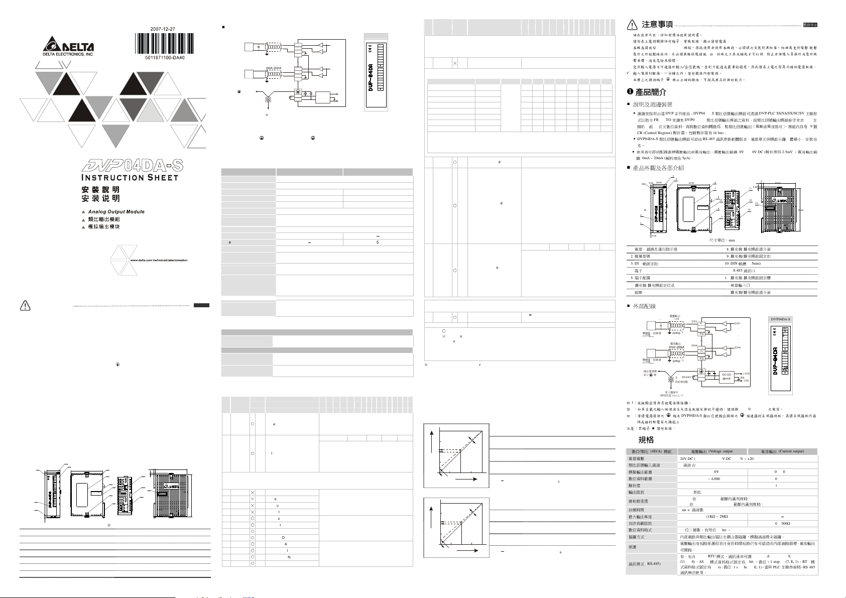
External Wiring
0V~+10V
*2
AC drive, recorder,
scale valve...
current output
AC drive, recorder,
scale valve...
terminal of
power module
class 3 grounding
Note 1: Please isolate analog output and other power wiring.
Note 2: If noise interference from loaded input terminal wiring is significant, please connect capacitor with 0.1 ~ 0.47µF
Note 3: Please connect power module terminal and analog output module terminal to system earth point and
Warning: DO NOT wire to the no function terminal ●.
Specifications
Digital/Analog (2D/A) module Voltage output Current output
Power supply voltage 24V DC (20.4V DC ~ 28.8V DC) (-15% ~ +20%)
Analog input channel 2 channels/each module
Analog output r ange 0 ~ 10V 0 ~ 20mA
Digital data range 0 ~ 4,000 0 ~ 4,000
Resolution 12 bits (1
Output impedance 0.5Ω or lower
(100
25V for noise filtering.
make system earth point be grounded or connects to machine cover.
Overall accuracy
Response time 3ms × channels
Max. output current 20mA (1KΩ ~ 2MΩ)
Tolerance carried impedance
Digital data format 2’s complementary of 16-bit, 13 significant bits.
Isolation method Isolation between digital area and analog area. But no isolation among
Protection
Communication mode
(RS-485)
Connect to DVP-PLC MPU in
series
V+
I+
shielding cable *1
FG
CH4
V+
I+
FG
shielding cable *1
DC24V
*3
system grounding
±0.5% of full scale of 25°C (77°F).
±1% of full scale during 0 ~ 55°C (32 ~ 131°F).
channels.
Voltage output has short circuit protection but a long period short circuit may
cause internal wire damage and current output break.
Yes, communication formats are (4,800/9,600/19,200/38,400/57,600/115,200
bps). Communication format: ASCII mode is 7 bits, even bit, 1 st op bit (7, E,
1). Communication format of RTU mode is 8 bits, even bit, 1 stop bit (8, E, 1).
When connecting to PLC MPU in series, RS-485 can’t be used.
If DVP04DA-S modules are connected to MPU, the modules are numbered
from 0 - 7. 0 is the closest and 7 is the furthest to the MPU. 8 modules is the
max and they DO NOT occupy any digital I/O points of the MPU.
.
.
.
.
.
CH4
AG
converter
=2.5mV) 12 bits (1
LSB
-
0 ~ 500Ω
DVP04DA-S
=5µA)
LSB
-
Others
Max. rated power
consumption
Operation/storage
Vibration/shock immunity
CR (Control Register)
RS-485
CR
#
address
#0 H’4032
#1 H’4033
CR#1 is used to set two internal ch annels working mode of analog output m odule. Every channel has four modes that
can be set individuall y. For example: if setting CH1 to mode 2 (b2 ~ b0 = 010), CH2 to mode 1 (b5 ~ b3 = 001). It needs to
set CR#1 to H’000A.
#6 H’4038
#7 H’4039
#8 H’403A
#9 H’403B
#18 H’4044
#19 H’4045
#20 H’4046
#21 H’4047
#24 H’404A
#25 H’404B
#26 H’404C
#27 H’404D
24V DC (20.4V DC ~ 28.8V DC) (-15% ~ +20%), 4W, supply from external
power.
Operation: 0°C ~ 55°C (temperature); 50 ~ 95% (humidity); pollution degree 2.
Storage: -25°C ~70°C (temperature); 5 ~ 95% (humidity).
International standards: IEC 61131-2, IEC 68-2-6 (TEST Fc)/IEC 61131-2 & IEC
68-2-27 (TEST Ea)
Latched Register name b15 b14 b13 b12 b11 b10 b9 b8 b7 b6 b5 b4 b3 b2 b1 b0
○
R Model type
○
R/W Output mode setting
╳
R/W CH1 output value
╳
R/W CH2 output value
╳
R/W CH3 output value
╳
R/W CH4 output value
○
R/W To adjust OFFSET value of CH1
○
R/W To adjust OFFSET value of CH2
○
R/W To adjust OFFSET value of CH3
○
R/W To adjust OFFSET value of CH4
○
R/W To adjust GAIN value of CH1
○
R/W To adjust GAIN value of CH2
○
R/W To adjust GAIN value of CH3
○
R/W To adjust GAIN value of CH4
Power supply
Environment
DVP-04DA model code=H’89.
User can read the data from program to check if there is
extension module.
Reserved CH4 CH3 CH2 CH1
Output mode setting: default setting is H’0000.
Mode 0: output voltage mode (0V ~ 10V).
Mode 1: output voltage mode (2V ~ 10V).
Mode 2: output current mode (4mA ~ 20mA).
Mode 3: output current mode (0mA ~ 20mA).
Mode 4: none use.
The output setting range of channel CH 1 ~ CH4 is K0 ~
K4,000. Default setting is K0 and unit i s LSB.
The setting range is KThe default setting is K0 and unit i s LSB.
It is used to set the GAIN valu e of CH ~ CH4.
The setting range is K0 ~ K4,00 0.
The default setting is K2,000 and uni t is LSB.
RS-485
CR
Latched Register name b1 5 b14 b13 b12 b11 b10 b9 b8 b7 b6 b5 b4 b3 b2 b1 b0
#
address
CR#18 ~ CR#27: Please be noticed that GAIN VALUE – OFFSET VALUE=+400
value difference comes up small (within range), the ou tput signal resolution is then sli m and the variation is definitely
larger. On the contrast, if the valu e difference exceeds the range, the output signal resolutio n becomes larger and the
variation is definitely smaller.
#30 H’4050
╳
R Error status
CR#30 is error code. Please r efer to the following chart.
Error description Content b15 ~ b8 b7 b6 b5 b4 b3 b2 b1 b0
Power source abnormal K1 (H’1) 0 0 0 0 0 0 0 1
Analog input value error K2 (H ’2) 0 0 0 0 0 0 1 0
Setting mode error K4 (H ’4) 0 0 0 0 0 1 0 0
Offset/gain error K8 (H’8) 0 0 0 0 1 0 0 0
Hardware malfunction K16 (H’10) 0 0 0 1 0 0 0 0
Digital range error K32 (H’20) 0 0 1 0 0 0 0 0
Average times setting error K64 (H’40) 0 1 0 0 0 0 0 0
Instruction error K128 (H’80)
Note: Each error code will have correspon ding bit (b0 ~ b7). Two or more errors may happe n at the same time. 0
means normal and 1 means having error.
error K2 and K32 will occur.
#31 H’4051
○
R/W Communication address settin g
#32 H’4052
#33 H’4053
Communication baud rate
○
R/W
setting
Reset to default setting and set
R/W
○
characteristics adjustable priorit y
Please refer to error code chart for detail .
Reserved
Used to set RS-485 communicati on address. The setting
range is from 01 to 254 and the default setting is K1.
Used to set communication baud rate (4,800 / 9,600 /
19,200 / 38,400 / 57,600 / 115,200 bps). Communicatio n
format: ASCII mode is 7 bits, even bit, 1 stop bit (7, E, 1).
Communication format of RTU mode is 8 bits, even bit, 1
stop bit (8, E, 1).
b2: 19,200 bps (bit/sec).
b3: 38,400 bps (bit/sec).
b4: 57,600 bps (bit/sec).
b5: 115,200 bps (bit/sec).
b6b14: exchange low and high byte of CRC check code
(RTU mode only).
b15: ASCII/RTU mode selection.
Output latched setting, default settin g H’0000.
Give CH1 setting for example:
1. When b0=0, user can set O FFSET and GAIN value of
2. b1 is used to check if characteristic register is latched.
3. When b2 is set to 1, all s ettings are reset to default
CR#33 is used to set the in ternal function priority. For example: characteristic register. Output latched functio n will save
output setting to the internal m emory before power loss.
#34 H’4054
#35 ~ #48 System used
Symbols: ○ means latched.
LSB (Least Significant Bit): 1. Voltage ou tput: 1
※
The corresponding parameters address H’4032 ~ H’4054 of CR#0 ~ CR#34 are pr ovided for user to read/
write data via RS-485.
A. Communication baud rate: 4,800/9,600/19,200/38,400/57,600/115,200 bps.
B. Communication format: ASCII mode is 7 bits, even bit, 1 stop bit (7, E, 1). Communication format of RTU
C. Function code: 03’H - read data from register. 06’H - write one word to register. 10’H - write multiple
R Software version.
○
╳
means not latched.
R means can read data by using FRO M instruction via RS-485.
W means can write data by using TO instruc tion via RS-485.
2. Current output: 1
=10V/8,000=2.5mV.
LSB
=20mA/4,000=5µA.
LSB
For example: H’010A means 1.0A.
mode is 8 bits, even bit, 1 stop bit (8, E, 1).
words to register.
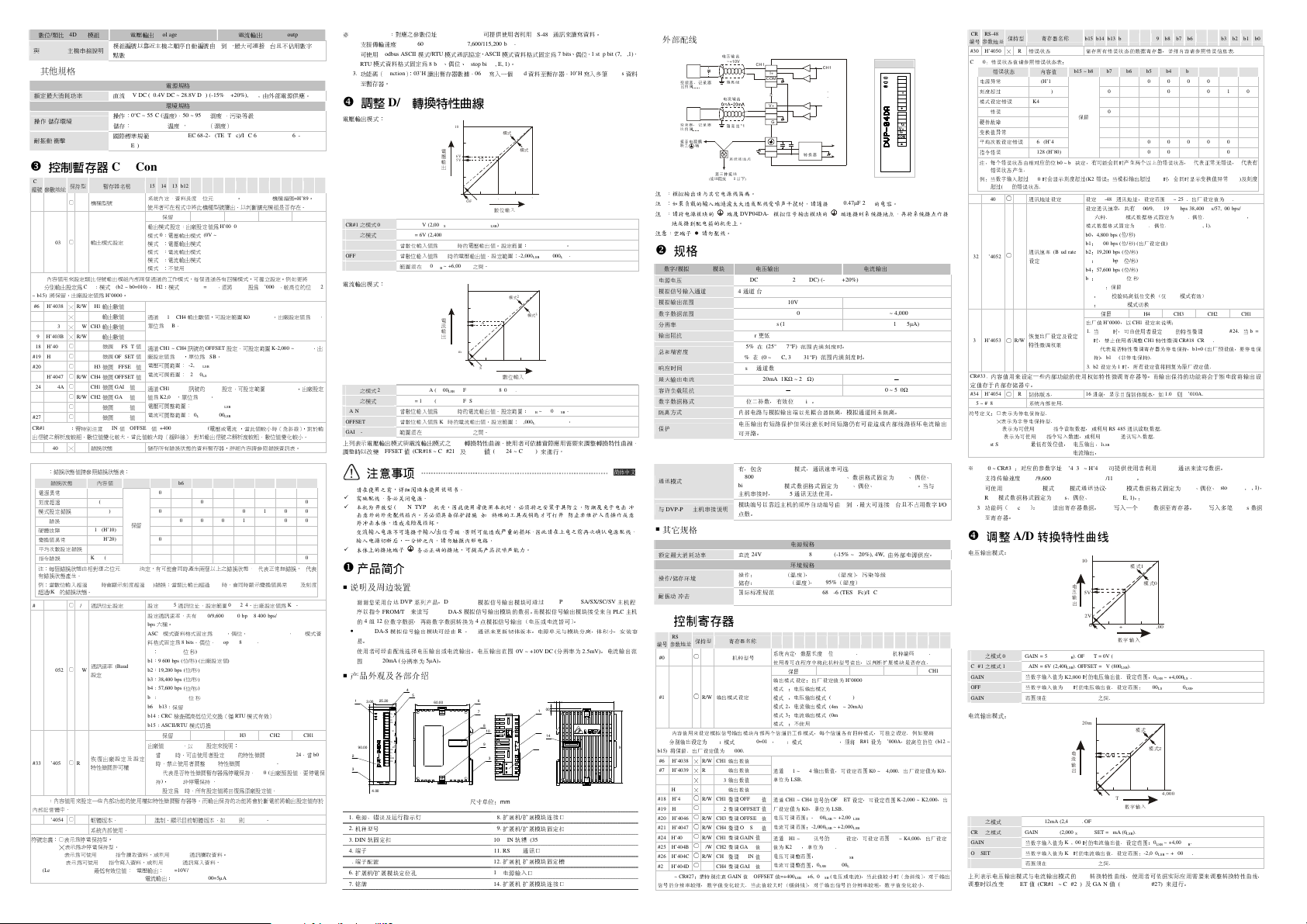
Adjust A/D Conversion Curve
~ +6,000
(voltage or current).If the
LSB
LSB
1 0 0 0 0 0 0 0
Reserved CH4 CH3 CH2 CH1
CH1 (CR#18, CR#24). When b0=1, inhibit user to adju st
OFFSET and GAIN value of CH1 (CR#18, CR#24).
b1=0 latched (default setting), b1 =1 not latched.
setting.
Voltage output mode:
voltage
output
10V
6V
GAIN
5V
2V
+2,00 0 + 4,000
OFFSE T
Mode 0 of CR#1: GAIN=5V (2,000
mode 1
Mode 1 of CR#1: GAIN=6V (2,400
mode 0
GAIN:
OFFSET:
GAIN-OFFSET: Setting range: +400
The setting range of voltage output value when digital
input value is K2,000 should be 0
The setting range of voltage output value when digital
input value is K0 should be -2,000
), OFFSET=0V (0
LSB
), OFFSET=2V (800
LSB
~ +6,000
LSB
LSB
LSB
LSB
~ +4,000
~ +2,000
LSB
.
).
).
LSB
LSB
LSB
Current output mode:
20mA
12mA
GAIN
10mA
current
output
4mA
0
+2,000 +4 ,000
OFFSET
The charts above are D/A conversion characteristic curve of voltage input mode and curr ent input mode. Users
can adjust conversion characteristic curve by changing OFFSET values (CR#18 ~ CR#21) and GAIN values
(CR#24 ~ CR#27) depend on application.
digital input
Mode 2 of CR#1: GAIN=12mA (2,400
mode 2
Mode 3 of CR#1: GAIN=10mA (2,000
mode 3
GAIN:
OFFSET:
GAIN-OFFSET: Setting range: +400
), OFFSET=4mA (800
LSB
), OFFSET=0mA (0
The setting range of current output when digital input
value is K2,000 should be 0
The setting range of cur rent output when digital input
value is K0 should be -2,000
LSB
~ +6,000
LSB
~ +4,000
LSB
LSB
~ +2,000
.
LSB
LSB
).
LSB
.
LSB
.
LSB
注意事項
請在使用之前,詳細 閱讀本使用說明書。
請勿在上電時觸摸任何端 子。實施配線,務必關 閉電源。
本機為開放型
(OPEN TYPE)
意外之外殼配線箱內。另必須具備保 護措施
擊本體,造成危險及損壞。
交流輸入電源不可連接於輸 入/出信號端,否則可能造 成嚴重的損壞,因此請在 上電之前再次確認電源配 線。
輸入電源切斷後,一分鐘 之內,請勿觸摸內部電 路。
本體上之接地端子
說明及週邊裝置
DVP04DA-S
產品外觀及各部介紹
1.
2.
3.
4.
5.
6.
7.
外部配線
註1:模擬輸出請與其他電 源線隔離。
註2:如果負載之輸入端 漣波太大造成配線受雜訊干 擾時,請連接
註3:請將電源模組之
注意:空端子
數位/類比
.
電源電壓
類比訊號輸入通道
.
模擬輸出範圍
數位資料範圍
解析度
輸出阻抗
總和精密度
).
回應時間
最大輸出電流
容許負載阻抗
數位資料格式
隔離方式
保護
通訊模式
務必正確的接地,可提 高產品抗雜訊能力。
產品簡介
謝謝您採用台達
DVP
式以指令
FROM/TO
類比信號輸出模組 可經由
1
25.20
3.00
90.00
4.00
軌固定扣
來讀寫
暫存器,每個暫存器 有
解析度為
4
V+
C
I+
H
COM
1
FG
V+
C
I+
H
COM
2
FG
●
V+
C
I+
H
COM
3
FG
V+
C
I+
H
COM
4
FG
●
機的4組12位元數位資料,再將數位資料轉換為4點類比信號輸出(電壓或電流皆可)。模組內具有49個
CR (Control Register)
易。
使用者可經由配線選擇電壓 輸出或電流輸出。電壓輸出範 圍
圍
0mA ~ 20mA (
2
3
電源、錯誤及運行指示 燈
機種型號
DIN
端子
端子配置
擴充機/擴充模組定位孔
銘牌
電壓輸出
0V~+10V
*2
隔離線
變頻器、記錄器
例閥..比 . ...
電流輸出
變頻器、記錄器
隔離線
例閥..比 . ...
接至電源模
之 組 端
第三種接地
( 地抗阻 00 以下接 1 )Ω
端及DVP04DA-S
地或接到配電箱之機殼 上。
請勿配線。
規格
(4D/A) 模組
4通道/台
0.5Ω or更低
3ms ×
16
(RS-485)
機殼,因此使用者使用 本機時,必須將之安裝於 具防塵、防潮及免於電擊/衝擊
系列產品。
DVP04DA-S
DVP04DA-S
5µA)。
(如:
特殊之工具或鑰匙才可打 開) 防止非維護人員操作或意外 衝
類比信號輸出模組可透 過
類比信號輸出模組之資 料。而類比信號輸出模組 接受來自
16 bits。
RS-485
通訊更新韌體版本。電源 單元與模組分離,體積 小,安裝容
0V ~ +10V DC (
5
*1
*1
DC24V
*3
系統接地點
24V DC (20.4V DC ~ 28.8V DC) (-15% ~ +20%)
±0.5% 在 (25°C, 77°F)
±1% 在 (0 ~ 55°C, 32 ~ 131°F)
位二補數,有效位
內部電路與類比輸出端 以光耦合器隔離,模擬通 道間未隔離。
電壓輸出有短路保護但須 注意長時間短路仍有可 能造成內部線路損壞,電流輸出
可開路。
有,包含
/115,200),ASCII
式資料格式固定為
通訊無法使用。
6
60.00
7
8
9
尺寸單位:
V+
I+
FG
CH4
V+
I+
FG
24-
類比信號輸出模組 之
電壓輸出
(Voltage output)
0 ~ 10V 0 ~ 20mA
0 ~ 4,000 0 ~ 4,000
12 bits (1
=2.5mV) 12 bits (1
LSB
通道數
10mA (1KΩ ~ 2MΩ)
-
11 bits。
ASCII/RTU
模式,通訊速率可選
模式資料格式固定 為
8 bits
11
12
10
13
3
mm
擴充機/擴充模組連介面
8.
擴充機/擴充模組固定扣
9.
DIN軌糟 (35mm)
10.
RS-485
通訊口
11.
擴充機/擴充模組固定槽
12.
電源輸入口
13.
擴充機/擴充模組連介面
14.
.
.
.
.
.
CH4
+15V
AG
轉換器
0.1 ~ 0.47µF 25V
端連接到系統接地點, 再將系統接點作接
範圍內滿刻度時。
範圍內滿刻度時。
7 bits
、偶位、
1 stop bit (8, E, 1)
(4,800/9,600/19,200/38,400/57,600
DVP-PLC SS/SA/SX/SC/SV
解析度為
2.5mV)
3.4
60.00
3.00
14
DVP04DA-S
之電容。
電流輸出
(Current output)
LSB
-
0 ~ 500Ω
、偶位、
1 stop bit (7, E, 1),RTU
。當與
PLC
主機串接時,
。電流輸出範
=5µA)
90.00
繁体中文
主機程
PLC
RS-485
主
模
Page 2
數位/類比
數位輸入
模式
0
V+
I+
COM
FG
V+
I+
COM
FG
I+
COM
FG
V+
I+
COM
FG
V+
0
(4D/A) 模組
與
DVP-PLC
主機串接說明
其他規格
額定最大消耗功率
操作/儲存環境
耐振動/衝擊
CR
編號
#0 H’4032
#1 H’4033
CR#1
CH4
~ b15)
#6 H’4038
#7 H’4039
#8 H’403A
#9 H’403B
#18 H’4044
#19 H’4045
#20 H’4046
#21 H’4047
#24 H’404A
#25 H’404B
#26 H’404C
#27 H’404D
CR#18 ~ CR#27
出信號之解析度較細,數位值變化較大。當此值較大時(緩斜 線),對於輸出信號之解析度較粗,數位值變化較小。
#30 H’4050
CR#30
#31 H’4051
#32 H’4052
#33 H’4053
CR#33
內部記憶體中。
#34 H’4054
#35 ~ #48
符號定義:○表示為停電保持型。
LSB (Least Significant Bit)
控制暫存器
RS-485
保持型 暫存器名稱
參數地址
○
R
○
R/W
內容值用來設定類比信號輸出模組內部兩個通道 的工作模式,每個通道各有四種模式,可獨立設定。例如要將
分別輸出設定為
將保留。出廠設定值為
╳
R/W CH1
╳
R/W CH2
╳
R/W CH3
╳
R/W CH4
○
R/W CH1微調OFFSET值
○
R/W CH2微調OFFSET值
○
R/W CH3微調OFFSET值
○
R/W CH4微調OFFSET值
○
R/W CH1微調GAIN值
○
R/W CH2微調GAIN值
○
R/W CH3微調GAIN值
○
R/W
:需特別注意
╳
R
:錯誤狀態值請參照錯誤狀態表:
錯誤狀態 內容值
電源異常
刻度超過
模式設定錯誤
O/G錯誤
硬體故障
變換值異常
平均次數設定錯誤
指令錯誤
注:每個錯誤狀態由相對應之位元
有錯誤狀態產生。
例:當數位輸入超過
超過
(K2)
的錯誤狀態。
○
R/W
○
R/W
○
R/W
:內容值用來設定一些內 部功能的使用權如特性微調暫 存器等。而輸出保持的功能將 會於斷電前將輸出設定值存於
○
R
╳表示為非停電保持型。
R
表示為可使用
W
表示為可使用TO指令寫入資料,或利用
電壓輸出
(Voltage output)
模組編號以靠近主機之 順序自動編號由0到7,最大 可連接8台且不佔用數字
點數
電源規格
直流
24V DC (20.4V DC ~ 28.8V DC) (-15% ~ +20%), 4W,
操作:
0°C ~ 55°C (溫度),50 ~ 95% (濕度)
儲存:
-25°C ~ 70°C (溫度),5 ~ 95%
國際標準規範
(TEST Ea)
環境規格
IEC 61131-2, IEC 68-2-6 (TEST Fc)/IEC 61131-2 & IEC 68-2-27
(濕度)
電流輸出
,污染等級
(Current output)
由外部電源供應。
2
CR (Control Register)
b15 b14 b13 b12 b11 b10 b 9 b8 b7 b6 b5 b4 b3 b2 b1 b0
機種型號
輸出模式設定
CH1
:模式
CH4微調GAIN值
錯誤狀態
K1 (H’1) 0 0 0 0 0 0 0 1
K2 (H’2) 0 0 0 0 0 0 1 0
K4 (H’4) 0 0 0 0 0 1 0 0
K8 (H’8) 0 0 0 0 1 0 0 0
K16 (H’10) 0 0 0 1 0 0 0 0
K32 (H’20) 0 0 1 0 0 0 0 0
K64 (H’40) 0 1 0 0 0 0 0 0
K128 (H’80)
4000
時會顯示刻度超過
通訊位址設定
通訊速率
設定
恢復 出廠 設定 及 設定
特性微調許可權
韌體版本。
系統內部使用。
FROM
最低有效位值:1.電壓輸出:
系統內定,資料長度8位元
使用者可在程式中將此機種型號讀出,以判斷擴充模組 是否存在。
保留
輸出模式設定:出廠設定值為
模式0:電壓輸出模式
模式1:電壓輸出模式
模式2:電流輸出模式
模式3:電流輸出模式
模式4:不使用
2 (b2 ~ b0=010),CH2
H’0000
輸出數值
輸出數值
輸出數值
輸出數值
GAIN值-OFFSET值=+400
(Baud rate)
指令讀取資料,或利用
:模式
。
通道
CH1 ~ CH4
單位為
LSB。
通道
CH1 ~ CH4
廠設定值為K0,單位為
電壓可調範圍:
電流可調範圍:
通道
CH1 ~ CH4
值為
K2,000
電壓可調整範圍:
電流可調整範圍:
儲存所有錯誤狀態的資料暫存器,詳細內容請參照錯誤 資訊表。
b15 ~ b8 b7 b6 b5 b4 b3 b2 b1 b0
保留
1 0 0 0 0 0 0 0
b0 ~ b7
決定,有可能會同時產生兩個以上之錯誤狀態,0代表正常無錯誤,1代表
(K2)
錯誤;當類比輸出超過
設定
RS-485
設定通訊速率,共有
bps
六種。
ASCII
模式資料格式固定為
料格式固定為
b0:4,800 bps (位/秒)
b1:9,600 bps (位/秒) (
b2:19,200 bps (位/秒)
b3:38,400 bps (位/秒)
b4:57,600 bps (位/秒)
b5:115,200 bps (位/秒)
b6 ~ b13
:保留
b14:CRC
b15:ASCII/RTU
保留
出廠值
H’0000,以CH1
1. 當b0=0
時,禁止使用者調整
2. b1
代表是否特性微調暫存器為停電保持,
持),
3. b2
設定為1時,所有設定值將回復為原廠設定值。
16
進制,顯示目前韌體版本,如
RS-485
1
LSB
2.
電流輸出:
(b7 ~ b0)。DVP04DA-S
CH4 CH3 CH2 CH1
H’0000
(0V ~ 10V)
(2V ~ 10V)
(4mA ~ 20mA)
(0mA ~ 20mA)
1 (b5 ~ b3=001)
,須將
輸出數值,可設定範圍
訊號的
OFFSET
LSB。
-2,000
~ +2,000
LSB
-2,000
~ +2,000
LSB
訊號的
GAIN
設定,可設定範圍
,單位為
LSB。
0
~ +4,000
LSB
LSB
0
~ +4,000
LSB
LSB
~ +6,000
(
電壓或電流),當此值較小時(急斜線),對於輸
LSB
LSB
10V
時,會同時顯示變換值異常
通訊位址,設定範圍
4,800/9,600/19,200 bps/38,400 bps/57,600 bps/115,200
7 bits
、偶位、
8 bits
、偶位、
1 stop bit (8, E, 1)。
出廠設定值
檢查碼高低位元交換(僅
模式切換
CH4 CH3 CH2 CH1
設定來說明:
時,可由使用者設定
b1=1 (
RS-485
=10V/4,000=2.5mV
1
LSB
CH1
非停電保持)。
通訊讀取資料。
通訊寫入資料。
=20mA/4,000=5µA
特性微調
CH1
CR#1設為H’000A
K0 ~ K4,000
設定,可設定範圍
LSB
LSB
01 ~ 254
。出廠設定值為K1。
1 stop bit (7, E, 1),RTU
)
RTU
模式有效)
的特性微調
CR#18, CR#24。
b1=0 (
1.0A則 H’010A。
機種編碼
,較高位的位
。出廠設定值為K0,
K-2,000 ~ K2,000
K0 ~ K4,000
CR#18, CR#24。當b0=1
出廠預設值,要停電保
(K32)
=H’89。
,出廠設定
及刻度
模式資
※
CR#0 ~ CR#34
1.
支援傳輸速度
2.
可使用
RTU
3.
功能碼(
至暫存器。
調整
I/O
電壓輸出模式:
CR#1
之模式
CR#1
之模式
GAIN
OFFSET
GAIN - OFFSET
CH1 ~
電流輸出模式:
(b12
,出
CR#1
之模式
CR#1
之模式
GAIN
OFFSET
GAIN - OFFSET
上列表示電壓輸出模式與 電流輸出模式之
調整時以
请在使用之前,详细 阅读本使用说明书。
实施配线,务必关闭电 源。
本机为开放型
击意外的外壳配线 箱内。另必须具备保 护措施
外冲击本体,造成危险及损 坏。
交流输入电源不可连 接于输入/出信号端,否则可能造成严重的损 坏,因此请在上 电之前再次确认电源配线 。
输入电源切断后,一分钟 之内,请勿触摸内部电 路。
本体上的接地端子
產品簡介
说明及周边装置
谢谢您采用台达
序以指令
的4组12位数字数据,再将数字数据 转换为4点模拟信号输出(电压 或电流皆可)。
DVP04DA-S
易。
使用者可经由配线选择电压 输出或电流输出。电 压输出范围
围
0mA ~ 20mA (
产品外观及各部介绍
1
90.00
2
3
1.
电源、错误及运行指示 灯
2.
机种型号
3. DIN
4.
端子
5.
端子配置
6.
扩展机/扩展模块定位孔
7.
铭牌
:對應之參數位址
Modbus ASCII模式/RTU
模式資料格式固定為
Function):03’H
D/A
0 GAIN = 5V (2,000
1 GAIN = 6V (2,400
2 GAIN = 12mA ( 2,400
3 GAIN = 10mA ( 2,000
改變
OFFSET值 (CR#18 ~ CR#21) 及GAIN值 (CR#24 ~ CR#27)
H’4032 ~ H’4054
4,800/9,600/19,200/38,400/57,600/115,200 bps。
8 bits
讀出暫存器數據。
轉換特性曲線
當數位輸入值為
當數位輸入值為K0時的電壓輸出值。設定範圍:
範圍須在
+400
LSB
當數位輸入值為
當數位輸入值為K0時的電流輸出值。設定範圍:
範圍須在
+400
LSB
可提供使用者利用
模式通訊協定,
ASCII
、偶位、
1 stop bit (8, E, 1)。
06’H
寫入一個
10V
電
壓
6V
GAI N
輸
5V
出
2V
0
+2 000,+4,0 00
OFF SET
). OFFSET = 0V (0
LSB
). OFFSET = 2V (800
LSB
K2,000
~ +6,000
電
流
輸
出
LSB
LSB
K2,000
~ +6,000
數位輸 入
).
LSB
LSB
時的電壓輸出值。設定範圍:
之間。
LSB
20 mA
12 mA
GA IN
10 mA
4m A
+2, 00 0 +4, 00 0
OF FSE T
). OFFSET = 4mA (800
). OFFSET = 0mA (0
D/A
LSB
時的電流輸出值。設定範圍:
之間。
LSB
轉換特性曲線,使用者可依據實際應用需要來 調整轉換特 性曲線,
注意事項
(OPEN TYPE)
机壳,因此使用者使用 本机时,必须将之 安装于具防尘、防潮及免 于电击/冲
(如:
务必正确的接地,可提 高产品抗噪声能力。
特殊的工具或钥匙才 可打开
DVP
系列产品。
DVP04DA-S
FROM/TO
来读写
DVP04DA-S
模拟信号输出模块可经 由
分辨率为
5µA)。
4
5
25.20
3.00
V+
C
I+
H
COM
1
FG
V+
C
I+
H
COM
2
FG
●
V+
C
I+
H
COM
3
FG
V+
C
I+
H
COM
4
FG
●
4.00
轨固定扣
10. DIN轨糟 (35mm)
12.
14.
13.
模拟信号输出模块可透 过
模拟信号输出模块的数 据。而模拟信号输出模块接受来 自
RS-485
通讯来更新韧体版本。电源单元与模块分 离,体积小,安装容
6
60.00
7
8
10
9
3
尺寸单位:
mm
8.
9.
11.
RS-485
通訊來讀寫資料。
模式資料格式固定 為
word
資料至暫存器。
模式
1
模式
0
).
0
~ +4,000
LSB
-2,000
~ +2,000
LSB
模式
2
3
).
LSB
).
0
~ +4,000
LSB
-2,000
~ +2,000
LSB
來進行。
DVP-PLC SS/SA/SX/SC/SV
0V ~ +10V DC (
3.00
11
12
14
13
扩展机/扩展模块连接口
扩展机/扩展模块固定扣
RS-485
通讯口
扩展机/扩展模块固定槽
电源输入口
扩展机/扩展模块连接口
7 bits
、偶位、
1 stop bit (7, E,1)
10’H
寫入多筆
。
LSB
。
LSB
。
LSB
。
LSB
)
防止非维护人员操 作或意
分辨率为
2.5mV)
3.4
60.00
words
資料
简体中文
主机程
PLC
主机
。电流输出范
90.00
外部配线
,
注1:模拟输出请与其它电 源线隔离。
注2:如果负载的输入端 涟波太大造成配线受噪声干 扰时,请连接
注3:请将电源模块的
地或接到配电箱的机壳 上。
注意:空端子
規格
数字/模拟
电源电压
模拟信号输入通道
模拟输出范围
数字数据范围
分辨率
输出阻抗
总和精密度
响应时间
最大输出电流
容许负载阻抗
数字数据格式
隔离方式
保护
通讯模式
与
DVP-PLC
其它规格
额定最大消耗功率
操作/储存环境
耐振动/冲击
控制寄存器
CR
RS-485
编号
参数地址
#0 H’4032
#1 H’4033
CR#1
内容值用来设定模拟信号输出模块内部两个信道的工作模 式,每个信道各有四种模式,可独立设定。例如要将
CH4
分别输出设定为
b15)
将保留。出厂设定值为
#6 H’4038
#7 H’4039
#8 H’403A
#9 H’403B
#18 H’4044
#19 H’4045
#20 H’4046
#21 H’4047
#24 H’404A
#25 H’404B
#26 H’404C
#27 H’404D
CR#18 ~ CR#27
信号的分辨率较细,数字值变化较大。当此值较大时(缓斜 线),对于输出信号的 分辨率较粗,数字值变化较小。
电压输 出
0V~+10V
*2
变频器 、记录 器
比例阀
..... .
变频器 、记录 器
..... .
比例阀
接至电 源模
块之 端
( )
接地阻抗 Ω以下
请勿配线。
(4D/A) 模块
24V DC (20.4V DC ~ 28.8V DC) (-15% ~ +20%)
4通道/台
0 ~ 10V 0 ~ 20mA
0 ~ 4,000 0 ~ 4,000
0.5Ω or更低
3ms ×
16
(RS-485)
主机串接说明
直流24V DC (20.4V DC ~ 28.8V DC) (-15% ~ +20%), 4W,
CH1
V+
I+
COM
隔离线
*1
FG
电流输 出
CH4
V+
I+
COM
FG
隔离线
*1
24+
DC24V
*3
24-
系统接 地点
第三种 接地
100
端及DVP04DA-S
模拟信号输出模块 的
电压输出
12 bits (1
±0.5% 在 (25°C, 77°F)
±1% 在 (0 ~ 55°C, 32 ~ 131°F)
通道数
20mA (1KΩ ~ 2MΩ)
位二补数,有效位
内部电路与模拟输出端 以光耦合器隔离,模拟通 道间未隔离。
电压输出有 短路保护但 须注意长时 间短路仍有 可能造成内 部线路损坏 电流输出
可开路。
有,包含
ASCII/RTU
(4,800/9,600/19,200/38,400/57,600/ 115,200)
bits (7, E, 1), RTU
主机串接时,
RS-485
模块编号以靠近主机的 顺序自动编号由0到7,最大可连接8台且不占用数字
点数。
操作:
0°C ~ 55°C
储存:
-25°C ~ 70°C
国际标准规范
IEC 61131-2, IEC 68-2-6 (TEST Fc)/IEC 61131-2 & IEC 68-2-27
(TEST Ea)
CH1
.
.
.
.
.
CH4
+15V
DC/DC
AG
转换器
-15V
0.1 ~ 0.47µF 25V
端连接到系统接地点, 再将系统接点作接
(Voltage output)
=2.5mV) 12 bits (1
LSB
范围内满刻度时。
-
0 ~ 500Ω
13 bits。
模式,通讯速率可选
模式数据格式固定为
通讯无法使用。
电源规格
环境规格
(温度),
(温度),
范围内满刻度时。
50 ~ 95%
(湿度),污染等级
5 ~ 95%
(湿度)
、数据格式固定为
8 bits
、偶位 、
CR
保持型 寄存器名称
○
R
○
R/W
CH1
╳
R/W CH1
╳
R/W CH2
╳
R/W CH3
╳
R/W CH4
○
R/W CH1微调OFFSET值
○
R/W CH2微调OFFSET值
○
R/W CH3微调OFFSET值
○
R/W CH4微调OFFSET值
○
R/W CH1微调GAIN值
○
R/W CH2微调GAIN值
○
R/W CH3微调GAIN值
○
R/W CH4微调GAIN值
:需特别注意
b15 b14 b13 b12 b11 b10 b9 b8 b7 b6 b5 b4 b3 b 2 b1 b0
机种型号
输出模式设定
:模式
2 (b2 ~ b0=010),CH2
H’0000。
输出数值
输出数值
输出数值
输出数值
GAIN值-OFFSET值=+400
系统内定,数据长度8位
使用者可在程序中将此机种型号读出,以判断扩展模块 是否存在。
输出模式设定:出厂设定值为
模式0:电压输出模式
模式1:电压输出模式
模式2:电流输出模式
模式3:电流输出模式
模式4:不使用
通道
CH1 ~ CH4
单位为
通道
CH1 ~ CH4
厂设定值为K0,单位为
电压可调范围:
电流可调范围:
通道
CH1 ~ CH4
值为
K2,000
电压可调整范围:
电流可调整范围:
(b7 ~ b0)。DVP04DA-S
保留
CH4 CH3 CH2 CH1
H’0000
(0V ~ 10V)
(2V ~ 10V)
(4mA ~ 20mA)
(0mA ~ 20mA)
:模式
1 (b5 ~ b3=001)
,须将
输出数值,可设定范围
LSB。
信号的
OFFSET
设定,可设定范围
LSB。
-2,000
~ +2,000
LSB
LSB
-2,000
~ +2,000
LSB
LSB
讯号的
GAIN
设定,可设定范围
,单位为
LSB。
0
~ +4,000
LSB
LSB
0
~ +4,000
LSB
LSB
~ +6,000
(
电压或电流),当此值较小时(急斜线),对于输出
LSB
LSB
CR#1设为H’000A
的电容。
电流输出
1 stop bit (8, E, 1)
K0 ~ K4,000
DVP04DA-S
(Current output)
=5µA)
LSB
-
7 bits
、偶位、
由外部电源供应。
2
机种编码
,较高位的位
。出厂设定值为K0,
K-2,000 ~ K2,000
K0 ~ K4,000
。当与
=H’89。
1 stop
(b12 ~
,出厂设定
CR
RS-485
保持型 寄存器名称
编号
参数地址
#30 H’4050
╳
CR#30
#31 H’4051
#32 H’4052
#33 H’4053
CR#33
定值存于内部存储器 中。
#34 H’4054
#35 ~ #48
符号定义:○表示为停电保持型。
LSB (Least Significant Bit)
※
PLC
I/O
电压输出模式:
CR#1
CR#1
GAIN
OFFSET
GAIN - OFFSET
电流输出模式:
CH1 ~
R
:错误状态值请参照错误状态表:
错误状态 内容值
电源异常
K1 (H ’1) 0 0 0 0 0 0 0 1
刻度超过
模式设定错误
K4 (H’4) 0 0 0 0 0 1 0 0
O/G错误 K8 ( H’8) 0 0 0 0 1 0 0 0
硬件故障
变换值异常
K32 (H’20) 0 0 1 0 0 0 0 0
平均次数设定错误
指令错误
K128 ( H’80)
注:每个错误状态由相对应的位
错误状态产生。
例:当数字输入超过
超过
(K2)
的错误状态。
○
R/W
○
R/W
R/W
○
:
内容值用来设定一些内部 功能的使用权如特性微 调寄存器等。而输出保持的功能 将会于断电前将输出设
R
○
╳
表示为非停电保持型。
R
表示为可使用
W
表示为可使用TO指令写入数据,或利用
CR#0 ~ CR#34
:对应的参数字址
1.
支持传输速度
2.
可使用
Modbus ASCII模式/RTU
RTU
模式数据格式固定为
3.
功能码(
Function):03’H
至寄存器。
調整
A/D
之模式
0 GAIN = 5V (2,000
之模式
1 GAIN = 6V (2,400
,出
CR#1
之模式
2 GAIN = 12mA ( 2,400
CR#1
之模式
3 GAIN = 10mA ( 2,000
GAIN
OFFSET
GAIN - OFFSET
上列表示电压输出模式与 电流输出模式的
调整时以
改变
OFFSET值 (CR#18 ~ CR#21) 及GAIN值 (CR#24 ~ CR#27)
b15 b14 b13 b12 b11 b10 b9 b8 b7 b6 b5 b4 b3 b 2 b1 b0
错误状态
储存所有错误状态的数据寄存器,详细内容请参照错误信息 表。
b15 ~ b8 b7 b6 b5 b4 b3 b2 b1 b0
K2 (H’2) 0 0 0 0 0 0 1 0
保留
K16 (H’10) 0 0 0 1 0 0 0 0
K64 (H’40) 0 1 0 0 0 0 0 0
4000
时会显示刻度超过
通讯地址设定 设定
通讯速率
设定
恢复出厂设定及设定
特性微调权限
韧体版本。
系统内部使用。
FROM
最低有效位值:1.电压输出:
4,800/9,600/19,200/38,400/57,600/115,200 b ps。
轉換特性曲線
当数字输入值为
当数字输入值为K0时的电压输出值。设定范围:
范围须在
当数字输入值为
当数字输入值为K0时的电流输出值。设定范围:
范围须在
b0 ~ b7
(Baud rate)
16
指令读取数据,或利用
8 bits
读出寄存器数据。
1 0 0 0 0 0 0 0
决定,有可能会同时产生两个以上的错误状态,0代表正常无错误,1代表有
(K2)
错误;当模拟输出超过
RS-485
通讯地址,设定范围
设定通讯速率,共有
bps
模式数据格式固定为
b0:4,800 bps (位/秒)
b1:9,600 bps (位/秒) (
b2:19,200 bps (位/秒)
b3:38,400 bps (位/秒)
b4:57,600 bps (位/秒)
b5:115,200 bps (位/秒)
b6 ~ b13
b14:CRC
b15:ASCII/RTU
出厂值
1. 当b0=0
2. b1
3. b2
2.
电流输出:
H’4032 ~ H’4054
模式通讯协议,
、偶位、
4,800/9,600/19,200 bps/38,400 bps/57,600 bps/115,200
六种。
ASCII
模式数据格式固定为
8 bits
、偶位、
出厂设定值
:保留
校验码高低位交换(仅
模式切换
保留
时,禁止使用者调整
代表是否特性微调寄存器为停电保持,
持),
设定为1时,所有设定值将回复为原厂设定值。
CH4 CH3 CH2 CH1
H’0000,以CH1
设定来说明:
时,可由使用者设定
CH1
b1=1 (
非停电保持)。
进制,显示目前韧体版本,如
RS-485
通讯读取数据。
RS-485
通讯写入数据。
1
=10V/4,000=2.5mV
LSB
1
=20mA/4,000=5µA
LSB
可提供使用者利用
ASCII
模式数据格式固定 为
1 stop bit (8, E, 1)。:
06’H
写入一个
word
+400
+400
K2,000
LSB
K2,000
LSB
LSB
LSB
~ +6,000
~ +6,000
10V
电
压
输
出
). OFFSET = 0V (0
). OFFSET = 2V (800
时的电压输出值。设定范围:
20mA
电
12mA
流
10mA
输
出
). OFFSET = 4mA (800
LSB
). OFFSET = 0mA (0
LSB
时的电流输出值。设定范围:
D/A
模式
1
GAIN
之间。
GAIN
OFFS ET
之间。
+2,000
数字 输入
).
LSB
).
LSB
模式
+2,00 0 + 4,000
数字输 入
).
LSB
).
LSB
模式
+4,000
-2,000
3
模式2
-2,000
6V
5V
2V
0
OFFSET
LSB
4mA
LSB
转换特性曲线,使用 者可依据实际应用需要来调整转换特性曲线,
10V
时,会同时显示变换值异常
01 ~ 254
。出厂设定值为K1。
7 bits
、偶位 、
1 stop bit (8, E, 1)。
)
RTU
模式有效)
CH1
的特性微调
特性微调
CR#18, CR#24。
b1=0 (
1.0A则H’010A。
RS-485
通讯来读写数据。
7 bits
数据至寄存器。
10’H
0
0
~ +4,000
。
LSB
LSB
~ +2,000
。
LSB
LSB
0
~ +4,000
。
LSB
LSB
~ +2,000
。
LSB
LSB
来进行。
(K32)
1 stop bit (7, E, 1),RTU
CR#18, CR#24。当b0=1
出厂预设值,要停电保
、偶位、
1 stop bit (7, E, 1)
写入多笔
words
及刻度
,
数据
 Loading...