

Page 1
3.3V 32-1250Mbps AnyRate™
CLOCK AND DATA RECOVERY
SY87701L
FEATURES
■ Industrial temperature range (–40°C to +85°C)
■ 3.3V power supply
■ Clock and data recovery from 32Mbps up to
1.25Gbps NRZ data stream
■ Complies with Bellcore, ITU/CCITT and ANSI
specifications for applications such as OC-1, OC-3,
OC-12, ATM, FDDI, etc.
■ Two on-chip PLLs: one for clock generation and
another for clock recovery
■ Selectable reference frequencies
■ Differential PECL high-speed serial I/O
■ Line receiver input: No external buffering needed
■ Link fault indication
■ 100K ECL compatible I/O
■ Available in 28-pin SOIC and 32-pin EP-TQFP
packages
DESCRIPTION
The SY87701L is a complete Clock Recovery and Data
Retiming integrated circuit for data rates from 32Mbps
up to 1.25Gbps NRZ. The device is ideally suited for
SONET/SDH/ATM and Fibre Channel applications and
other high-speed data transmission systems.
Clock recovery and data retiming is performed by
synchronizing the on-chip VCO directly to the incoming
data stream. The VCO center frequency is controlled by
the reference clock frequency and the selected divide
ratio. On-chip clock generation is performed through the
use of a frequency multiplier PLL with a byte rate source
as reference.
The SY87701L also includes a link fault detection
circuit.
APPLICATIONS
■ SONET/SDH/ATM OC-1, OC-3, OC-12, OC-24
■ Fibre Channel, Escon
■ Gigabit Ethernet/Fast Ethernet
■ Proprietary architecture up to 1.25Gbps
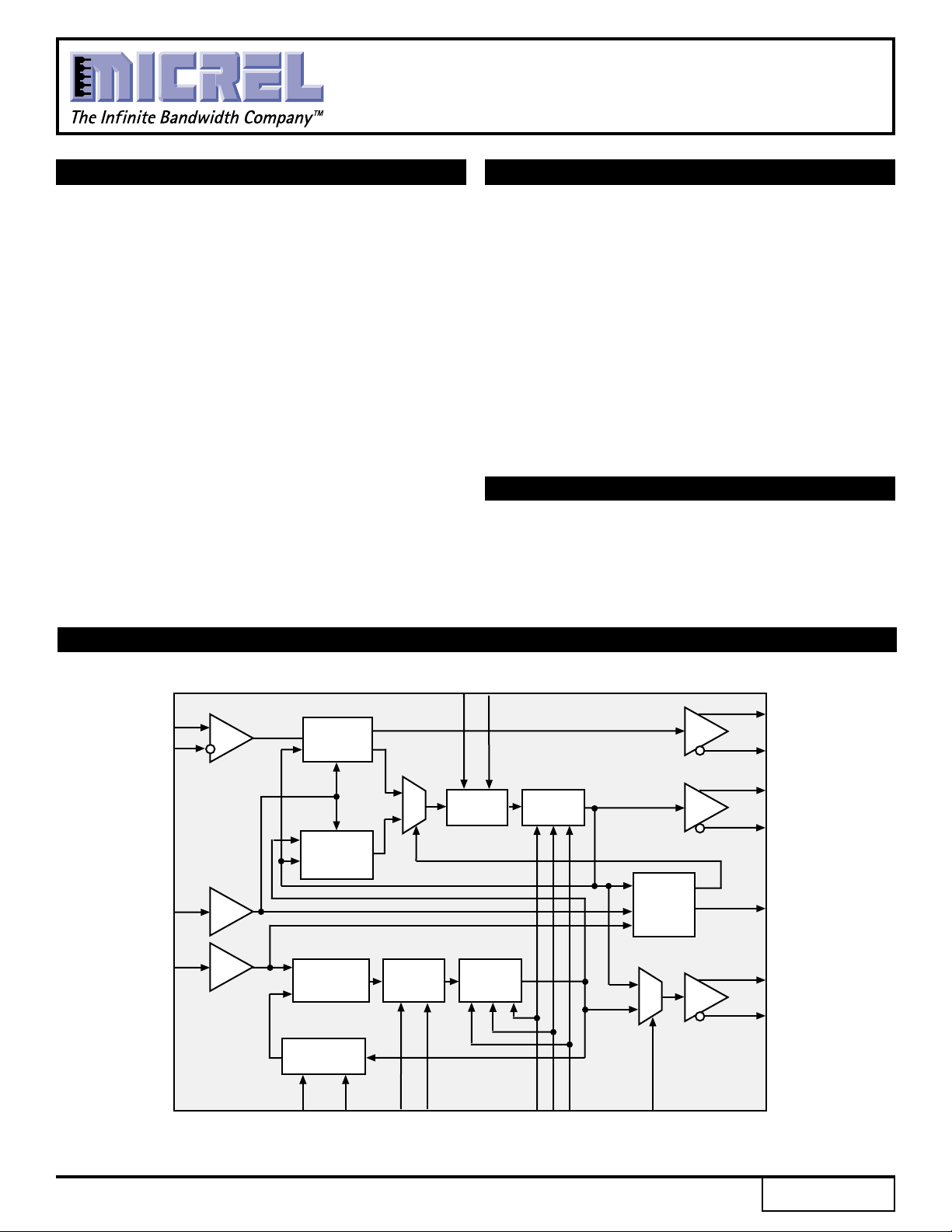
BLOCK DIAGRAM
RDINP
(PECL)
RDINN
CD
(PECL)
REFCLK
(TTL)
PHASE
DETECTOR
PHASE/
FREQUENCY
DETECTOR
PHASE/
FREQUENCY
DETECTOR
DIVIDER
BY 8, 10, 16, 20
0
1
CHARGE
PUMP
PLLR P/N
CHARGE
PUMP
VCO
SY87701L
VCO
LINK
FAULT
DETECTOR
1
0
RDOUTP
(PECL)
RDOUTN
RCLKP
(PECL)
RCLKN
LFIN
(TTL)
TCLKP
(PECL)
TCLKN
V
CC
VCCA
VCCO
GND
AnyRate™ is a trademark of Micrel, Inc.
DIVSEL 1/2
(TTL)
PLLS P/N
1
FREQSEL 1/2/3
(TTL)
CLKSEL
(TTL)
Rev.: B Amendment: /0
Issue Date:
September 2000
Page 2
Micrel
1
2
3
4
5
6
7
8
24
23
22
21
20
19
18
17
NC
RDINP
RDINN
FREQSEL1
REFCLK
FREQSEL2
FREQSEL3
NC
RDOUTP
RDOUTN
VCCO
RCLKP
RCLKN
VCCO
TCLKP
TCLKN
9
10
11 12 13 14 15 16
CLKSEL
PLLRP
PLLRN
GND
GND
GNDA
PLLSN
PLLSP
32
31
30 29 28 27 26 25
DIVSEL2
CD
VCC
VCC
VCCA
VCCA
LFIN
DIVSEL1
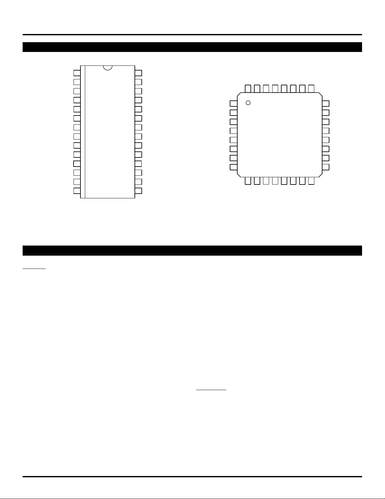
Top Vie w
EP-TQFP
H32-1
PIN CONFIGURATION
SY87701L
1VCCA
LFIN
2
DIVSEL1
FREQSEL1
REFCLK
FREQSEL2
FREQSEL3
RDINP
RDINN
N/C
10
PLLSP TCLKN1811
PLLSN CLKSEL1712
GND PLLRP1613
GND PLLRN1514
3
4
5
6
7
8
9
PIN DESCRIPTIONS
Top Vie w
SOIC
Z28-1
28 VCC
CD
27
DIVSEL2
26
RDOUTP
25
RDOUTN
24
VCCO
23
RCLKP
22
RCLKN
21
VCCO
20
TCLKP
19
INPUTS
RDINP, RDINN [Serial Data Input] Differential PECL.
These built-in line receiver inputs are connected to the
differential receive serial data stream. An internal receive
PLL recovers the embedded clock (RCLK) and data
(RDOUT) information. The incoming data rate can be within
one of eight frequency ranges depending on the state of
the FREQSEL pins. See “Frequency Selection” Table.
REFCLK [Reference Clock] TTL input.
This input is used as the reference for the internal
frequency synthesizer and the “training” frequency for the
receiver PLL to keep it centered in the absence of data
coming in on the RDIN inputs.
CD [Carrier Detect] PECL Input.
PLL and can be driven by the carrier detect output of optical
modules or from external transition detection circuitry. When
this input is HIGH the input data stream (RDIN) is recovered
normally by the Receive PLL. When this input is LOW the
data on the inputs RDIN will be internally forced to a constant
LOW, the data outputs RDOUT will remain LOW, the Link
Fault Indicator output LFIN forced LOW and the clock
recovery PLL forced to lock onto the clock frequency
generated from REFCLK.
This input controls the recovery function of the Receive
FREQSEL1, ..., FREQSEL3 [Frequency Select] TTL
Inputs.
These inputs select the output clock frequency range as
shown in the “Frequency Selection” Table.
DIVSEL1, DIVSEL2 [Divider Select] TTL Inputs.
These inputs select the ratio between the output clock
frequency (RCLK/TCLK) and the REFCLK input frequency
as shown in the “Reference Frequency Selection” Table.
CLKSEL [Clock Select] TTL Input.
This input is used to select either the recovered clock of
the receiver PLL (CLKSEL =HIGH) or the clock of the
frequency synthesizer (CLKSEL = LOW) to the TCLK
outputs.
OUTPUTS
LFIN [Link Fault Indicator] TTL Output.
This output indicates the status of the input data stream
RDIN. Active HIGH signal is indicating when the internal
clock recovery PLL has locked onto the incoming data
stream. LFIN will go HIGH if CD is HIGH and RDIN is within
the frequency range of the Receive PLL (1000ppm). LFIN
is an asynchronous output.
2
Page 3

Micrel
SY87701L
RDOUTP, RDOUTN [Receive Data Output] Differential
PECL.
These ECL 100K outputs represent the recovered data
from the input data stream (RDIN). This recovered data is
specified against the rising edge of RCLK.
RCLKP, RCLKN [Clock Output] Differential PECL.
These ECL 100K outputs represent the recovered clock
used to sample the recovered data (RDOUT).
TCLKP, TCLKN [Clock Output] Differential PECL.
These ECL 100K outputs represent either the recovered
clock (CLKSEL = HIGH) used to sample the recovered data
(RDOUT) or the transmit clock of the frequency synthesizer
(CLKSEL = LOW).
PLLSP, PLLSN [Clock Synthesis PLL Loop Filter]
External loop filter pins for the clock synthesis PLL.
PLLRP, PLLRN [Clock Recovery PLL Loop Filter]
External loop filter pins for the receiver PLL.
POWER & GROUND
VCC Supply Voltage
VCCA Analog Supply Voltage
VCCO Output Supply Voltage
GND Ground
NC No Connect
NOTE:
1. V
CC, VCCA, VCCO must be the same value.
(1)
(1)
(1)
FUNCTIONAL DESCRIPTION
Clock Recovery
Clock Recovery, as shown in the block diagram generates
a clock that is at the same frequency as the incoming data
bit rate at the Serial Data input. The clock is phase aligned
by a PLL so that it samples the data in the center of the
data eye pattern.
The phase relationship between the edge transitions of
the data and those of the generated clock are compared by
a phase/frequency detector. Output pulses from the detector
indicate the required direction of phase correction. These
pulses are smoothed by an integral loop filter. The output of
the loop filter controls the frequency of the Voltage Controlled
Oscillator (VCO), which generates the recovered clock.
Frequency stability without incoming data is guaranteed
by an alternate reference input (REFCLK) that the PLL locks
onto when data is lost. If the Frequency of the incoming
signal varies by greater than approximately 1000ppm with
respect to the synthesizer frequency, the PLL will be declared
out of lock, and the PLL will lock to the reference clock.
The loop filter transfer function is optimized to enable the
PLL to track the jitter, yet tolerate the minimum transition
density expected in a received SONET data signal. This
transfer function yields a 30µs data stream of continuous
1's or 0's for random incoming NRZ data.
The total loop dynamics of the clock recovery PLL
provides jitter tolerance which is better than the specified
tolerance in GR-253-CORE.
Lock Detect
The SY87701L contains a link fault indication circuit which
monitors the integrity of the serial data inputs. If the received
serial data fails the frequency test, the PLL will be forced to
lock to the local reference clock. This will maintain the correct
frequency of the recovered clock output under loss of signal
or loss of lock conditions. If the recovered clock frequency
deviates from the local reference clock frequency by more
than approximately 1000ppm, the PLL will be declared out
of lock. The lock detect circuit will pull the input data stream
in an attempt to reacquire lock to data. If the recovered
clock frequency is determined to be within approximately
1000ppm, the PLL will be declared in lock and the lock
detect output will go active.
3
Page 4
Micrel
y
CHARACTERISTICS
SY87701L
Performance
The SY87701L PLL complies with the jitter specifications
proposed for SONET/SDH equipment defined by the Bellcore
Specifications: GR-253-CORE, Issue 2, December 1995 and
ITU-T Recommendations: G.958 document, when used with
differential inputs and outputs.
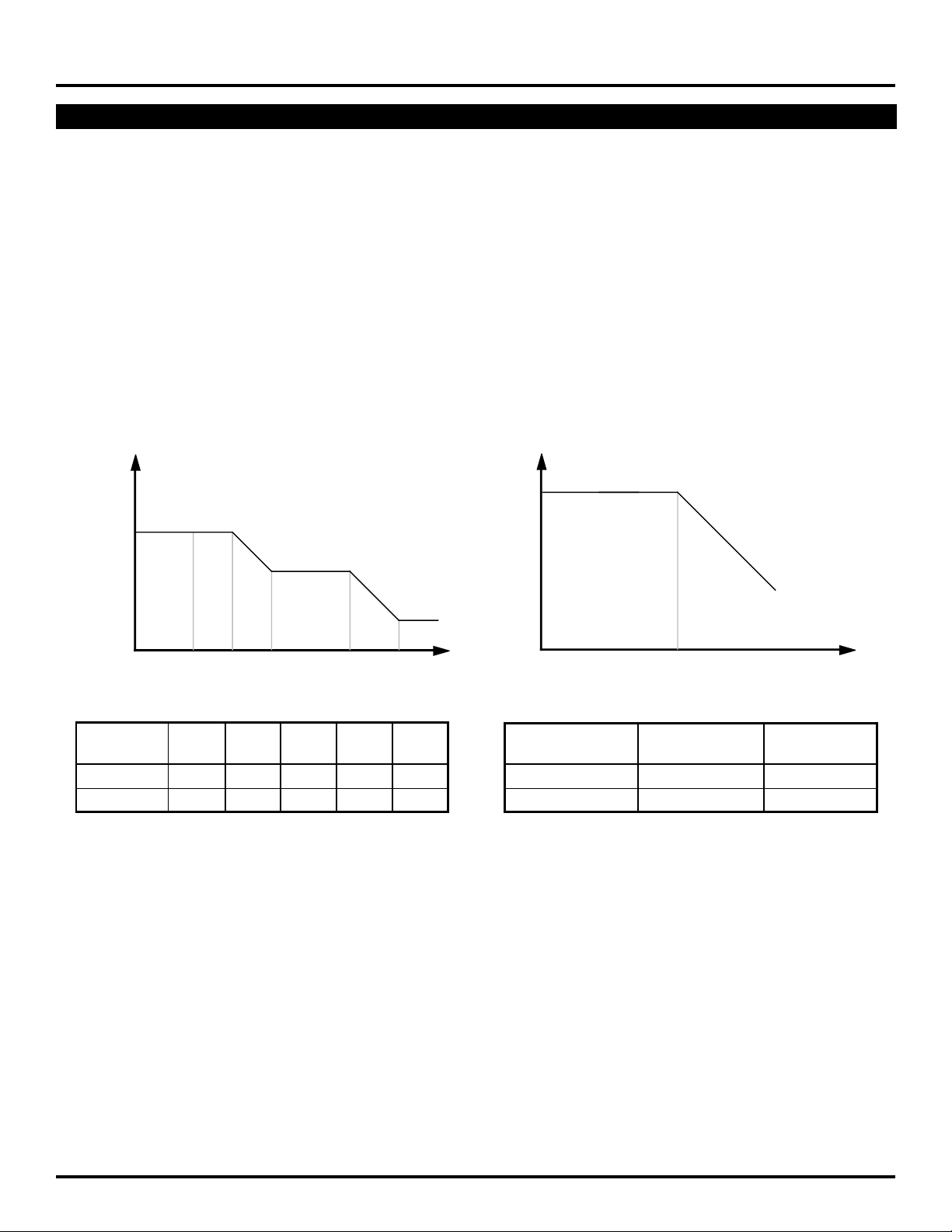
Input Jitter Tolerance
Input jitter tolerance is defined as the peak-to-peak
amplitude of sinusoidal jitter applied on the input signal that
causes an equivalent 1dB optical/electrical power penalty.
SONET input jitter tolerance requirement condition is the
input jitter amplitude which causes an equivalent of 1dB
power penalty.
A
15
1.5
(UI p-p)
Sinusoidal Input
Jitter Amplitude
0.40
-20dB/decade
-20dB/decade
Jitter Transfer
Jitter transfer function is defined as the ratio of jitter on
the output OC-N/STS-N signal to the jitter applied on the
input OC-N/STS-N signal versus frequency. Jitter transfer
requirements are shown in Figure 2.
Jitter Generation
The jitter of the serial clock and serial data outputs shall
not exceed .01 U.I. rms when a serial data input with no
jitter is presented to the serial data inputs.
Jitter Transfer (dB)
0.1
-20dB/decade
-20
Acceptable
Range
f0 f1 f2 f4 ft
Frequency
OC/STS-N f0 f1 f2 f3 ft
Level (Hz) (Hz) (Hz) (kHz) (kHz)
3 10 30 300 6.5 65
12 10 30 300 25 250
Figure 1. Input Jitter Tolerance
fc
Frequenc
OC/STS-N fc P
Level (kHz) (dB)
3 130 0.1
12 225 0.1
Figure 2. Jitter Transfer
4
Page 5

Micrel
FREQUENCY SELECTION TABLE
FREQSEL1 FREQSEL2 FREQSEL3 fVCO/fRCLK fRCLK Data Rates (Mbps)
0 0 0 1 750 – 1250
0 0 1 2 375 – 625
0 1 0 4 188 – 313
0 1 1 6 125 – 208
1 0 0 8 94 – 157
1 0 1 12 63 – 104
1 1 0 16 47 – 78
1 1 1 24 32 – 52
SY87701L
REFERENCE FREQUENCY SELECTION
DIVSEL1 DIVSEL2 fRCLK/fREFCLK
00 8
01 10
10 16
11 20
LOOP FILTER COMPONENTS
R5
PLLSP PLLSN
SONET Wide Range
R5 = 80Ω R5 = 350Ω
C3 = 1.5µF
(X7R Dielectric) C3 = 0.47µF (X7R Dielectric)
(1)
C3
ABSOLUTE MAXIMUM RATINGS
(1, 2)
Symbol Rating Value Unit
VCC Power Supply –0.5 to +7.0 V
VI Input Voltage –0.5 to VCC V
I
OUT Output Current mA
–Continuous 50
–Surge 100
Tstore Storage Temperature –65 to +150 °C
TA Operating Temperature –40 to +85 °C
JA Thermal Resistance 80 single °C/W
θ
@still air layer board,
46 multi-layer
NOTES:
1. Permanent device damage may occur if ABSOLUTE MAXIMUM RATINGS
are exceeded. This is a stress rating only and functional operation is not
implied at conditions other than those detailed in the operational sections
of this data sheet. Exposure to ABSOLUTE MAXIMUM RATING conditions
for extended periods may affect device reliability.
2. Airflow of 500LFPM recommended.
R6
PLLRP PLLRN
C4
SONET Wide Range
R6 = 50Ω R6 = 680Ω
C4 = 1.0µF (X7R Dielectric) C4 = 0.47µF (X7R Dielectric)
NOTE:
1. Suggested Values. Values may vary for different applications.
5
Page 6

Micrel
DC ELECTRICAL CHARACTERISTICS
Symbol Parameter Min. Typ. Max. Unit Condition
VCC Power Supply Voltage 3.15 3.3 3.45 V
CC Power Supply Current — 170 230 mA
I
PECL 100K DC ELECTRICAL CHARACTERISTICS
VCC = VCCO = VCCA = 3.3V ±5%; TA = –40°C to +85°C
Symbol Parameter Min. Typ. Max. Unit Condition
VIH Input HIGH Voltage VCC - 1.165 — VCC - 0.880 V
VIL Input LOW Voltage VCC - 1.810 — VCC - 1.475 V
IIL Input LOW Current 0.5 ——µAVIN = VIL(Min.)
VOH Output HIGH Voltage VCC - 1.075 — VCC - 0.830 V 50Ω to VCC –2V
OL Output LOW Voltage VCC - 1.860 — VCC - 1.570 V 50Ω to VCC –2V
V
TTL DC ELECTRICAL CHARACTERISTICS
VCC = VCCO = VCCA = 3.3V ±5%; TA = –40°C to +85°C
SY87701L
Symbol Parameter Min. Typ. Max. Unit Condition
VIH Input HIGH Voltage 2.0 — VCC V
VIL Input LOW Voltage ——0.8 V
IH Input HIGH Current –175 ——µAVIN = 2.7V, VCC = Max.
I
——+100 µAVIN = VCC, VCC = Max.
IIL Input LOW Current –300 ——µAVIN = 0.5V, VCC = Max.
VOH Output HIGH Voltage 2.0 ——VIOH = –0.4mA
VOL Output LOW Voltage ——0.5 V IOL = 4mA
OS Output Short Circuit Current 15 — 100 mA VOUT = 0V (maximum 1sec)
I
AC ELECTRICAL CHARACTERISTICS
VCC = VCCO = VCCA = 3.3V ±5%; TA = –40°C to +85°C
Symbol Parameter Min. Typ. Max. Unit Condition
fVCO VCO Center Frequency 750 — 1250 MHz fREFCLK * Byte Rate
∆f
VCO VCO Center Frequency — 5 — % Nominal
Tolerance
tACQ Acquisition Lock Time ——15 µs
tCPWH REFCLK Pulse Width HIGH 4 ——ns
tCPWL REFCLK Pulse Width LOW 4 ——ns
tir REFCLK Input Rise Time — 0.5 2 ns
tODC Output Duty Cycle (RCLK/TCLK) 45 — 55 % of UI
tr, tf ECL Output Rise/Fall Time 100 — 500 ps 50Ω to VCC –2 (20% to 80%)
tskew Recovered Clock Skew –200 — +200 ps
tDV Data Valid 1/(2*fRCLK) – 200 ——ps
DH Data Hold 1/(2*fRCLK) – 200 ——ps
t
6
Page 7

Micrel
TIMING WAVEFORMS
SY87701L
REFCLK
RCLK
RDOUT
t
ODC
t
CPWL
t
CPWH
t
ODC
t
t
DV
SKEW
tDH
7
Page 8

Micrel
APPLICATION EXAMPLE
SY87701L
GND
RDIN
Capacitor Pads
(1206 format)
C1
C2
See T able 1
GND
2N2222A
LED
D2
R3 R4
VCC
R10
Q1
R9
VCC
VCC
R2R1
GND
LOOP FILTER
NETWORK
REFCLK
(TTL)
NC
DPDT
Slide Switch
120Ω
R23
1.5µF
0.1µF
80Ω
C3
GND
14
C13
8
SW1
123456
1
VCCA
2
LFIN
3
DIVSEL1
RDINP
4
5
RDINN
FREQSEL1
6
REFCLK
7
8
FREQSEL2
FREQSEL3
9
N/C
10
R5
11
PLLSP
12
PLLSN
13
GND
GND
14
XTAL
Oscillator
1
7
VCC
CD
DIVSEL2
RDOUTP
RDOUTN
VCCO
RCLKP
RCLKN
VCCO
TCLKP
TCLKN
CLKSEL
PLLRP
PLLRN
28
27
26
25
24
23
22
21
20
19
18
17
16
15
(R17 - R22)
5kΩ x 6
50Ω
R6
C4
1.0µF
VCC
0.1µF
R11
R12
Ferrite Bead
BLM21A102
FB1
22µFC70.1µFC622µF
C9
C8
0.1µF
0.1µF
0.1µF
0.1µF
0.1µF
0.1µF
If VCC = +5V:
R9 through R14 = 330
R14
R16
R13
R15
If VCC = +3.3V:
R9 through R14 = 220
C10
C11
C12
VCC
C5
C14
C15
C16
C17
C18
C19
0.1µF
0.1µF
0.1µF
0.1µF
Stand Off
VCC
Pin 1 (VCCA)
Pin 28 (VCC)
Pin 23 (VCCO)
Pin 20 (VCCO)
DIODE D1
VCC
1N4148
R7
J1
R8
Ω
Ω
For AC coupling only For DC mode only
C1 = C2 = 0.1µF C1 = C2 = Shorted
R1 = R2 = 680Ω R1 = R2 = 130Ω
R3 = R4 = 1kΩ R3 = R4 = 82Ω
Table 1.
NOTE:
1. C5 and C10–C12 are decoupling capacitors and should be kept as close
to the power pins as possible.
8
Page 9

Micrel
Material List
SY87701L
For Bypass and AC coupling capacitor, high quality factor
(High Q) capacitors are recommended. This will optimize
the performance of the device in high frequency domain.
Description Component Part No.
SY87700L/SY87700V/SY87701L/SY87701V U1
80Ω PLLS+,
1.5µF PLLS–,
50Ω PLLR+,
1.0µF PLLR–,
5kΩ or 4.7kΩ Pull Up Resistor x 6,
330Ω or 220Ω (see schematic) Output Pull Down Resistor,
4.7KΩ Pull Up Resistor,
130Ω Pull Up Resistor,
12kΩ Pull Down Resistor,
12kΩ
120Ω
0.1µF AC Coupling Capacitors x 6,
Tantalum, 22µF, 16V Decoupling Capacitor,
0.1µF Decoupling Capacitors x 7,
Murata BLM21A102F Ferrite Bead,
1N4148 Diode,
Johnson SMAs, ID#142-0701-201 SMAs x 9
6-pin Dip switch SW1
The suggested dielectric characteristics for these capacitors
are NPO and/or COG. AVX is a suggested provider of
electronic components. www.avxcorp.com
(1, 2)
R5
C3
R6
C4
R17 – R22
R11 – R16
R7
R9
R8
R10
R23
C1, C2, C14 – C19
C6, C8
C5, C7, C9 – C13
FB1
D1
DPDT Slide Switch
LED
NOTES:
1. For VCC = 3.3V
R8 = 12kΩ; R = 130Ω
2. For VCC = 5.0V
R8 = 24kΩ; R9 = 200Ω
PRODUCT ORDERING CODE
Ordering Package Operating
Code Type Range
SY87701LZI Z28-1 Industrial
SY87701LHI H32-1* Industrial
*Contact factory for availability.
9
Page 10

Micrel
28 LEAD SOIC .300" WIDE (Z28-1)
SY87701L
Rev. 02
10
Page 11

Micrel
32 LEAD EPAD TQFP (DIE UP) (H32-1)
SY87701L
Rev. 01
11
Page 12

Micrel
SY87701L
MICREL-SYNERGY 3250 SCOTT BOULEVARD SANTA CLARA CA 95054 USA
TEL + 1 (408) 980-9191 FAX + 1 (408) 914-7878 WEB http://www.micrel.com
This information is believed to be accurate and reliable, however no responsibility is assumed by Micrel for its use nor for any infringement of patents or
other rights of third parties resulting from its use. No license is granted by implication or otherwise under any patent or patent right of Micrel Inc.
© 2000 Micrel Incorporated
12
 Loading...