

Page 1

SONET OC-12/OC-3
CLOCK SYNTHESIZER
FEATURES DESCRIPTION
ClockWorks™
SY89426
■ Single chip source for 622.08MHz and 155.52MHz
clocks
■ 622.08MHz output is differential PECL, 155.52MHz
output is single-ended PECL
■ TTL/CMOS compatible inputs and reference output
■ SONET compliant jitter performance (≤0.01UI)
■ Choice of three reference frequencies
■ Only 395mW (typ)
■ Complies with Bellcore, CCITT and ANSI standards
■ Single +5 volt power supply
■ Fully compatible with industry standard 10KH I/O
levels
■ Available in 28-pin PLCC package
TYPICAL APPLICATION
Micrel-Synergy's SY89426 Multi-Output Phase Locked
Loop (PLL) is a SONET compliant clock generator providing
622.08MHz, 155.52MHz and retimed reference clock
outputs. The PLL produces low jitter OC-12/STS-12 and
OC-3/STS-3 rate clocks from an input reference clock of
38.88, 51.84, or 77.76MHz. Additionally, the input reference
clock is retimed and provided as a TTL/CMOS compatible
output, which may be disabled to minimize switching noise.
The SY89426 operates from a single +5 volt supply, and
requires only a simple series RC loop filter.
Coupling Micrel-Synergy's advanced PLL technology
with our proprietary ASSET™ bipolar process has produced
a clock generator IC which exceeds applicable Bellcore
and ANSI specifications, while setting a new standard for
performance and flexibility.
PIN CONFIGURATION
CLOCK
IN
0.1uF
1000Ω
RFCK
(TTL)
FLTRN
FLTRP
SEL39
(TTL)
SEL78
(TTL)
+5V
VCC
SY89426
GND
+5V
VCCO
RST
(TTL)
CK622P
(PECL)
CK622N
CK155
(PECL)
RETRFCK
(TTL)
DISC
(TTL)
+3V
+3V
2X 50Ω
622.08MHz
CLOCK OUT
50Ω
155.52MHz
CLOCK OUT
RETIMED
REFOUT
GND
GND
SEL39
SEL78
RFCK
CC
V
NC
CC
V
FLTRN
FLTRP
RST
24 23 22 21 20 19
25
26
27
28
1
2
3
4
567891011
GND
PLCC
TOP VIEW
J28-1
NC
GND
NC
CC
V
RETRFCK
NC
GND
DISC
18
17
16
15
14
13
12
GND
VCC
CC
V
CK622P
CK622N
V
CCO
CK155
GND
Rev.: F Amendment: /0
1
Issue Date: July, 1999
Page 2
Micrel
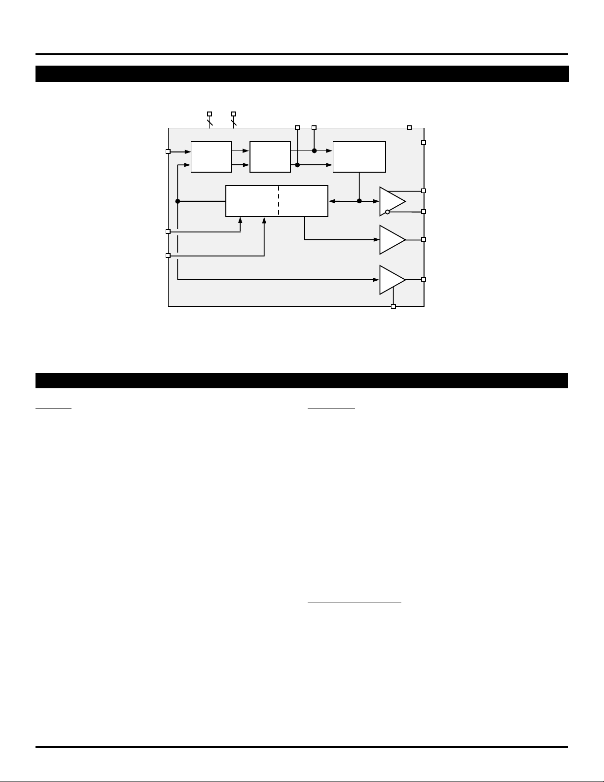
FUNCTIONAL BLOCK DIAGRAM
V
CCA
GND
57
FLTRP/N
V
ClockWorks™
SY89426
CCO
PIN DESCRIPTION
INPUTS
RFCK
(TTL)
SEL39
(TTL)
SEL78
(TTL)
Φ/f
CHG
PUMP
FEEDBACK
÷ 2/3/4
DIVIDER
÷ 4
OUTPUTS
622MHz
VCO
RST
(TTL)
CK622P
(PECL)
CK622N
CK155
(PECL)
RETRFCK
(TTL)
DISC
(TTL)
RFCK [Reference Clock] TTL
Reference clock IN. (38.88, 51.84 or 77.76MHz).
SEL39 [38.88MHz Select] TTL
Logic HIGH on this pin denotes a 38.88MHz input reference
clock. Tie to logic LOW if input is not 38.88MHz.
SEL78 [77.76MHz Select] TTL
Logic HIGH on this pin denotes a 77.76MHz input reference
clock. Tie to logic LOW if input is not 77.76MHz.
RST [Reset] TTL
Tie to logic LOW for normal operation; logic HIGH forces reset
of internal Phase Detector & feedback dividers.
FLTRP, FLTRN [Loop Filter, Pos & Neg] Analog
Connect a series RC loop filter between these pins. The
suggested RC values are 500Ω and 0.1µF, as shown in the
Typical Application.
DISC [Disable Clock] TTL
Logic HIGH on this pin disables the Retimed Reference Clock
output RETRFCK); if this output is not required, it is
recommended that it be disabled to reduce switching noise. A
logic LOW enables the output.
CK622P, CK622N [622 Clock Output] Differential PECL.
622.08MHz output clock from PLL B.
CK155 [155 Clock Out] Single-ended PECL
155.52MHz output clock.
RETRFCK [Retimed Reference Clock Out] TTL
An output clock with the same frequency as the input Reference
Clock (RFCK) and a 45-55% duty cycle. This output is derived
by dividing the 622.08MHz output by the appropriate factor
(e.g., divide by 16 for a 38.88MHz inout reference; divide by
12 for 51.84Mhz in; or divide by 8 for 77.76MHz in).
POWER & GROUND
VCC +5V for internal circuits.
VCCO +5V for PECL outputs.
GND Ground (0 volts).
2
Page 3
Micrel
ClockWorks™
SY89426
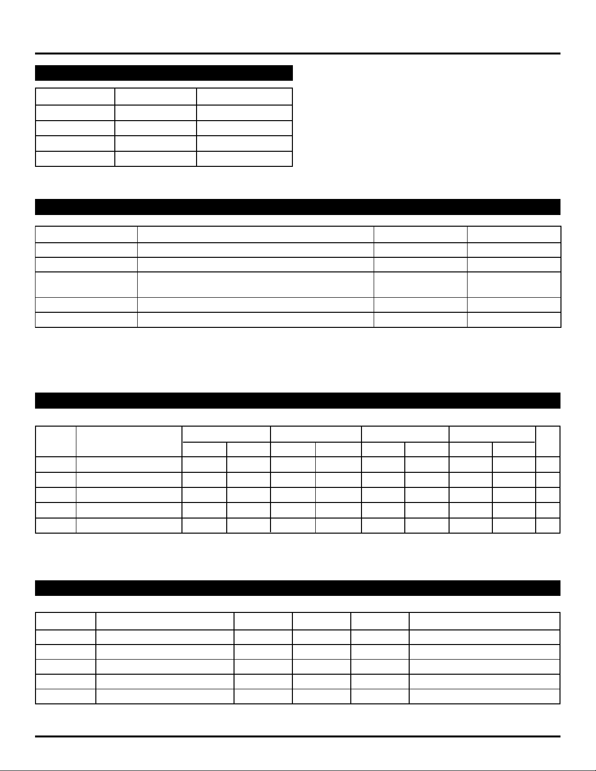
REFERENCE FREQUENCY SELECTION
(1)
SEL39 SEL78 fRFCK
0 0 51.84
0 1 77.76
1 0 38.88
1 1 77.76
NOTE:
1. Airflow greater than 500lfpm is maintained.
ABSOLUTE MAXIMUM RATINGS
(1), (2)
Symbol Parameter Rating Unit
VCC Power Supply 0 to +7 V
VI Input Voltage 0 to VCC V
IOUT Output Current –Continuous 50 mA
–Surge 100
TA Operating Temperature Range –40 to +85 °C
T
store Storage Temperature Range –65 to +150 °C
NOTES:
1. Permanent device damage may occur if ABSOLUTE MAXIMUM RATINGS are exceeded. This is a stress rating only and functional operation is not
implied at conditions other than those detailed in the operational sections of this data sheet. Exposure to ABSOLUTE MAXIMUM RATING conditions
for extended periods may affect device reliability.
2. Airflow greater than 500lfpm is maintained.
PECL DC ELECTRICAL CHARACTERISTIC
(1), (2)
VCC = VCCO = +5V ± 5%; GND = 0V; TA = –40°C to 85°C
TA = –40°CTA = 0°CTA = +25°CTA = +85°C
Symbol Parameter Min. Max. Min. Max. Min. Max. Min. Max. Unit
VOH Output HIGH Voltage
VOL Output LOW Voltage
VIH Input HIGH Voltage
VIL Input LOW Voltage
I
IL Input LOW Current 0.5 — 0.5 — 0.5 — 0.3 — µA
NOTES:
1. Forcing one input at a time. Apply VIH (Max) or VIL (Min) to all other inputs.
2. Airflow greater than 500lfpm is maintained.
TTL DC ELECTRICAL CHARACTERISTICS
V
CC
-1130
V
CC
-2000
(1)
V
CC
-1230
(1)
V
CC
-1950
V
CC
-840
V
CC
-1070
V
CC
-1600
V
CC
-2000
V
CC
-890
V
CC
-1170
V
CC
-1500
V
CC
-1950
(1)
V
CC
-790
V
CC
-1030
V
CC
-1580
V
CC
-2000
V
CC
-840
V
CC
-1130
V
CC
-1480
V
CC
-1950
V
CC
-760
V
CC
-960
V
CC
-670
V
CC
-1580
V
CC
-2000
V
CC
-1545
V
CC
-810
V
CC
-1060
V
CC
-1480
V
CC
-1950
V
CC
-720
V
CC
-1445
VCC = VCCO = +5V ± 5%; GND = 0V; TA = –40°C to 85°C
Symbol Parameter Min. Max. Unit Condition
VOH Output HIGH Voltage 2.4 — VIOH = –2mA
VOL Output LOW Voltage — 0.5 V IOL = 4mA
IOS Output Short Circuit Current –150 –60 mA VOUT = 0
VIH Input HIGH Voltage 2.0 — V —
V
IL Input LOW Voltage — 0.8 V —
NOTE:
1. Airflow greater than 500lfpm is maintained.
mV
mV
mV
mV
3
Page 4
Micrel
ClockWorks™
SY89426
DC ELECTRICAL CHARACTERISTICS — TTL
DC ELECTRICAL CHARACTERISTICS
(1)
VCC = VCCO = +5V ± 5%; GND = 0V; TA = –40°C to 85°C
Symbol Parameter Min. Typ. Max. Unit Condition
IEE Internal Operating Current — 79 120 mA
IOUT Termination Output Current — 11 — mA 50Ω to Vcc -2, 50% duty cycle
NOTE:
1. Airflow greater than 500lfpm is maintained.
AC ELECTRICAL CHARACTERISTICS
(1)
VCC = VCCO = +5V ± 5%; GND = 0V; TA = –40°C to 85°C
Parameter Min. Typ. Max. Units Condition
VCO Center Frequency 622.08 ±1% MHz Nominal
Reference Clock (RFCK)
Frequency Tolerance
Reference Clock (RFCK) Input Duty Cycle 45 — 55 % of UI
Reference Clock (RETRFCK) Output Duty Cycle 40 — 60 % of UI 15pF load
Acquisition Lock Time —— 15 µsec
TTL Output Rise/Fall Time —— 2 ns 10% to 90% of amplitude, 15pF load
PECL Output Rise/Fall Time —— 500 ps 10% to 90%, 50Ω load, 5pF cap
CK622 Output Duty Cycle 45 — 55 % of UI
CK155 Output Duty Cycle 45 — 55 % of UI
tRST – RST pulse width 1 ——µsec
tp622 Static Phase Offset of CK622 190 400 600 ps
tp155 Static Phase Offset of CK155 –250 –400 –750 ps
tpREF Static Phase Offset of RETRFCK — +3.5 — ns
NOTE:
1. Airflow greater than 500lfpm is maintained.
— ±20 — ppm 77.76MHz
— ±20 — ppm 51.84MHz
— ±10 — ppm 38.88MHz
DC ELECTRICAL CHARACTERISTICS — TTL
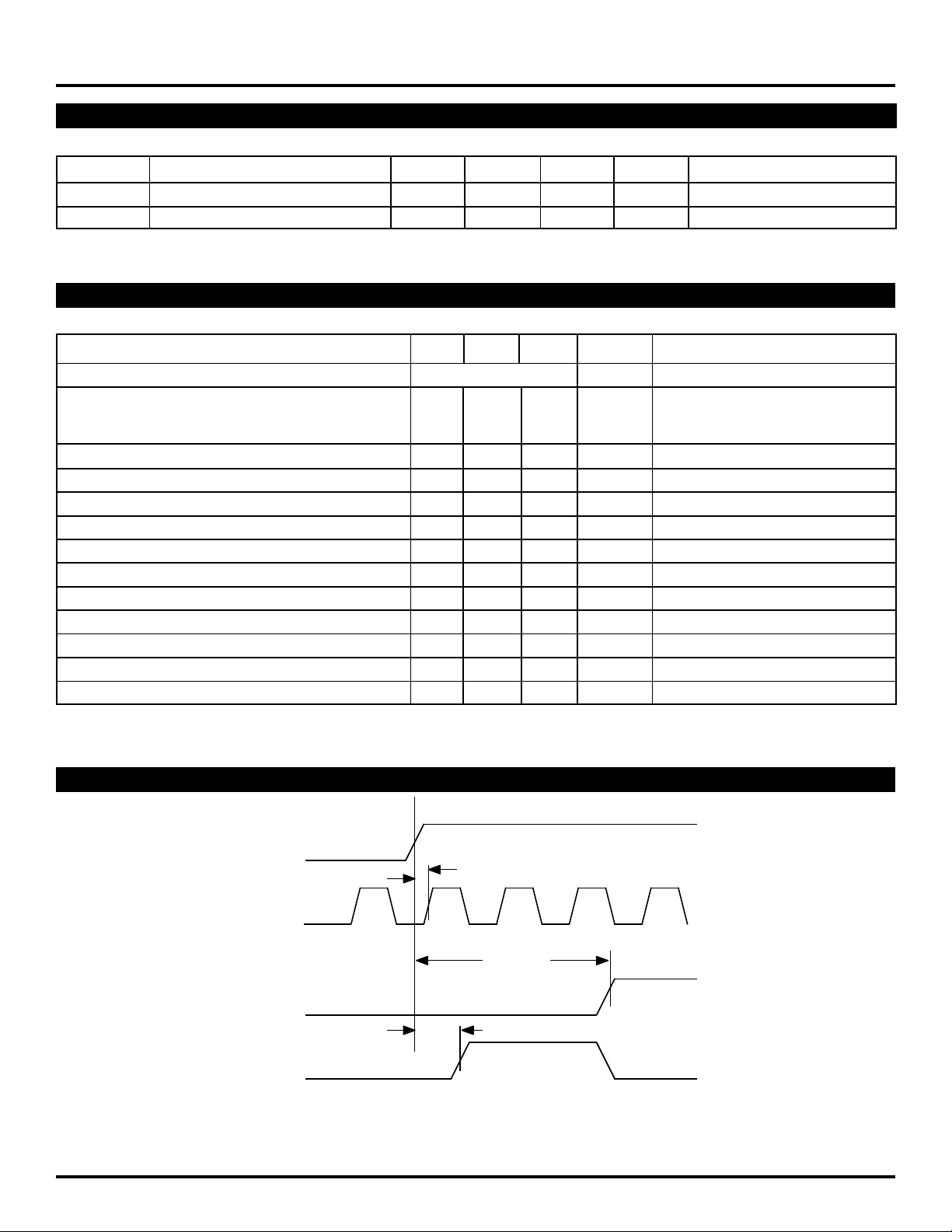
TIMING WAVEFORM
RFCK
Input
CK622
Output
RETRFCK
Output
CK155
Output
NOTE:
1. Does not apply to 52MHz reference
tp 622
tp 155
4
tp REF
(1)
Page 5
Micrel
JITTER GENERATION
ClockWorks™
SY89426
Jitter Generation Definition
Bellcore TR-NWT-000499 (Issue 4), section 7.3.3 "Jitter
generation is the process whereby jitter appears at the output
port of an individual unit of digital equipment in the absence of
applied input jitter."
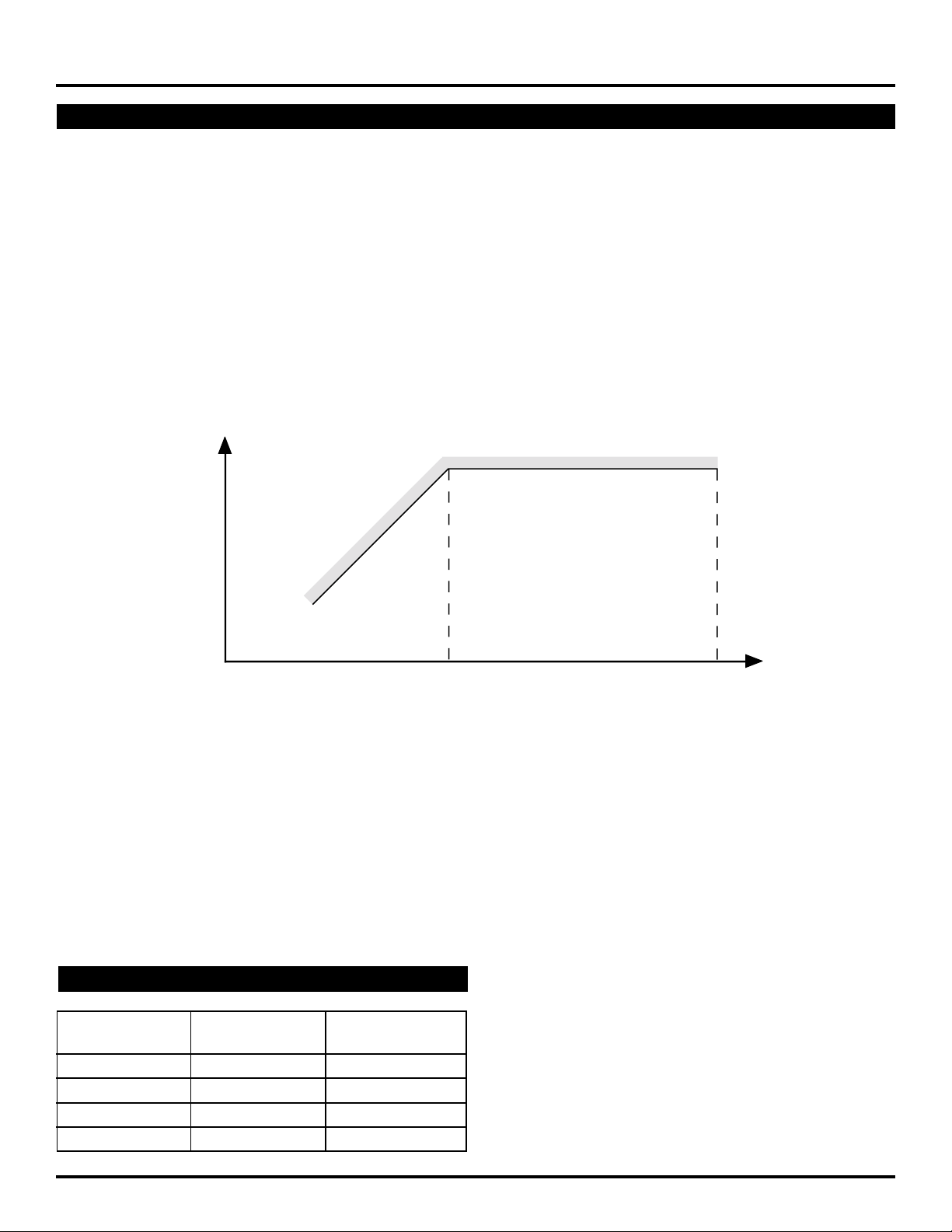
SONET OC-12 Category II Jitter Generation Measurement Filter Characteristics
UI (rms)
0.01
+20dB/decade
Jitter Generation Requirement
Bellcore TA-NWT-000253 (Issue 2), section 5.6.5.2 "For
Category II interfaces, jitter generation shall not exceed 0.01
UI rms. For OC-N and STSX-N interfaces, a high-pass
measurement filter with a 12kHz cutoff frequency shall be
used." The low-pass cutoff frequency of the measurement
filter shall be higher than 5MHz.
The characteristic of the measurement filter is shown
below.
PRODUCT ORDERING CODE
Ordering Package Operating
Code Type Range
SY89426JC J28-1 Commercial
SY89426JCTR J28-1 Commercial
SY89426JI J28-1 Industrial
SY89426JITR J28-1 Industrial
12kHz
Figure 1
Frequency
5MHz
(minimum)
5
Page 6
Micrel
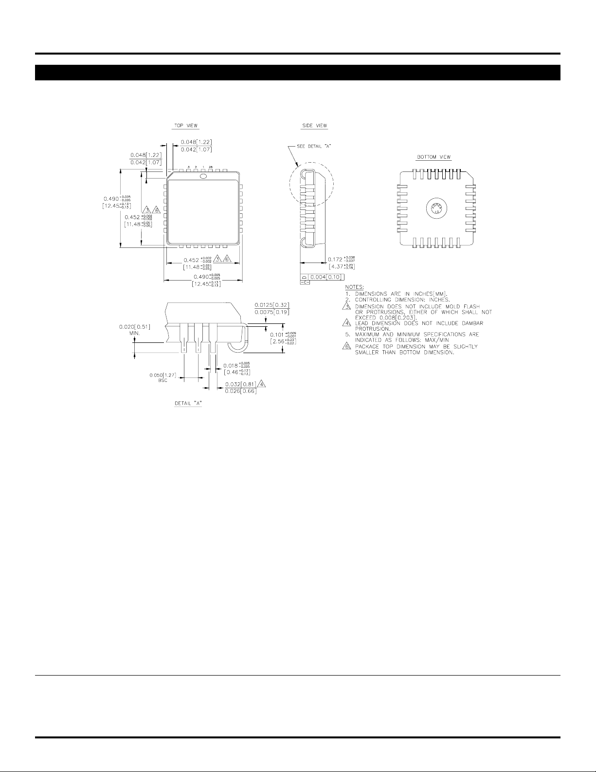
28 LEAD PLCC (J28-1)
ClockWorks™
SY89426
Rev. 03
MICREL-SYNERGY 3250 SCOTT BOULEVARD SANTA CLARA CA 95054 USA
TEL + 1 (408) 980-9191 FAX + 1 (408) 914-7878 WEB http://www.micrel.com
This information is believed to be accurate and reliable, however no responsibility is assumed by Micrel for its use nor for any infringement of patents or
other rights of third parties resulting from its use. No license is granted by implication or otherwise under any patent or patent right of Micrel Inc.
© 2000 Micrel Incorporated
6
 Loading...