

Page 1
查询SY89228UMG供应商
General Description
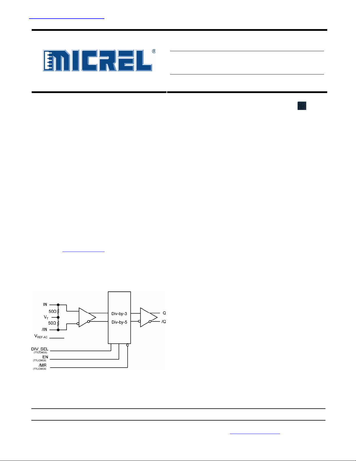
The SY89228U is a precision, low jitter 1GHz ÷3, ÷5
clock divider with an LVPECL output. A unique FailSafe Input (FSI) protection prevents metastable
output conditions when the input clock voltage swing
drops significantly below 100mV or input is removed.
The differential input includes Micrel’s unique, 3-pin
internal termination architecture that allows the input
to interface to any differential signal (AC- or DCcoupled) as small as 100mV (200mV
level shifting or termination resistor networks in the
signal path. The outputs are 800mV, 100Kcompatible LVPECL with fast rise/fall times
guaranteed to be less than 270ps.
The SY89228U operates from a 2.5V ±5% or 3.3V
±10% supply and is guaranteed over the full
industrial temperature range of –40°C to +85°C. The
SY89228U is part of Micrel’s high-speed, Precision
®
Edge
product line.
All support documentation can be found on Micrel’s
web site at: www.micrel.com
.
) without any
PP
Block Diagram
SY89228U
1GHz Precision, LVPECL ÷3, ÷5 Clock Divider
with Fail-Safe Input and Internal Termination
Precision Edge®
Features
• Accepts a high-speed input and provides a precision
÷3 and ÷5 sub-rate, LVPECL output
• Fail-Safe Input
– Prevents oscillations when input is invalid
• Guaranteed AC performance over temperature and
supply voltage:
– DC-to >1.0GHz throughput
– < 1500ps Propagation Delay (In-to-Q)
– < 270ps Rise/Fall times
• Ultra-low jitter design:
– <1ps
– <1ps
– <10ps
– <0.7ps
• Unique patented internal termination and VT pin
accepts DC- and AC-coupled inputs (CML, PECL,
LVDS)
• Wide input voltage range VCC to GND
• 800mV LVPECL output
• 46% to 54% Duty Cycle(÷ 3)
• 47% to 53% Duty Cycle(÷ 5)
• 2.5V ±5% or 3.3V ±10% supply voltage
• -40°C to +85°C industrial temperature range
• Available in 16-pin (3mm x 3mm) MLF
random jitter
RMS
cycle-to-cycle jitter
RMS
total jitter (clock)
PP
MUX crosstalk induced jitter
RMS
®
package
Applications
• Fail-safe clock protection
Markets
• LAN/WAN
• Enterprise servers
Precision Edge is a registered trademark of Micrel, Inc.
MLF and MicroLeadFrame are registered trademarks of Amkor Technology.
Micrel Inc. • 2180 Fortune Drive • San Jose, CA 95131 • USA • tel +1 (408) 944-0800 • fax + 1 (408) 474-1000 • http://www.micrel.com
August 2007
• ATE
• Test and measurement
M9999-080707-A
or (408) 955-1690
Page 2
Micrel, Inc. SY89228U
Ordering Information
(1)
Part Number
SY89228UMG MLF-16 Industrial
SY89228UMGTR
Notes:
1. Contact factory for die availability. Dice are guaranteed at T
2. Tape and Reel.
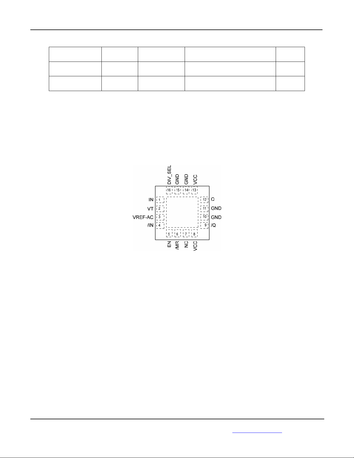
Pin Configuration
Package
Type
(2)
MLF-16 Industrial
Operating
Range
Package Marking
228U with
Pb-Free bar-line Indicator
228U with
Pb-Free bar-line Indicator
= 25°C, DC Electricals Only.
A
Lead
Finish
NiPdAu
Pb-Free
NiPdAu
Pb-Free
16-Pin MLF® (MLF-16)
August 2007 M9999-080707-A
2
or (408) 955-1690
Page 3
Micrel, Inc. SY89228U
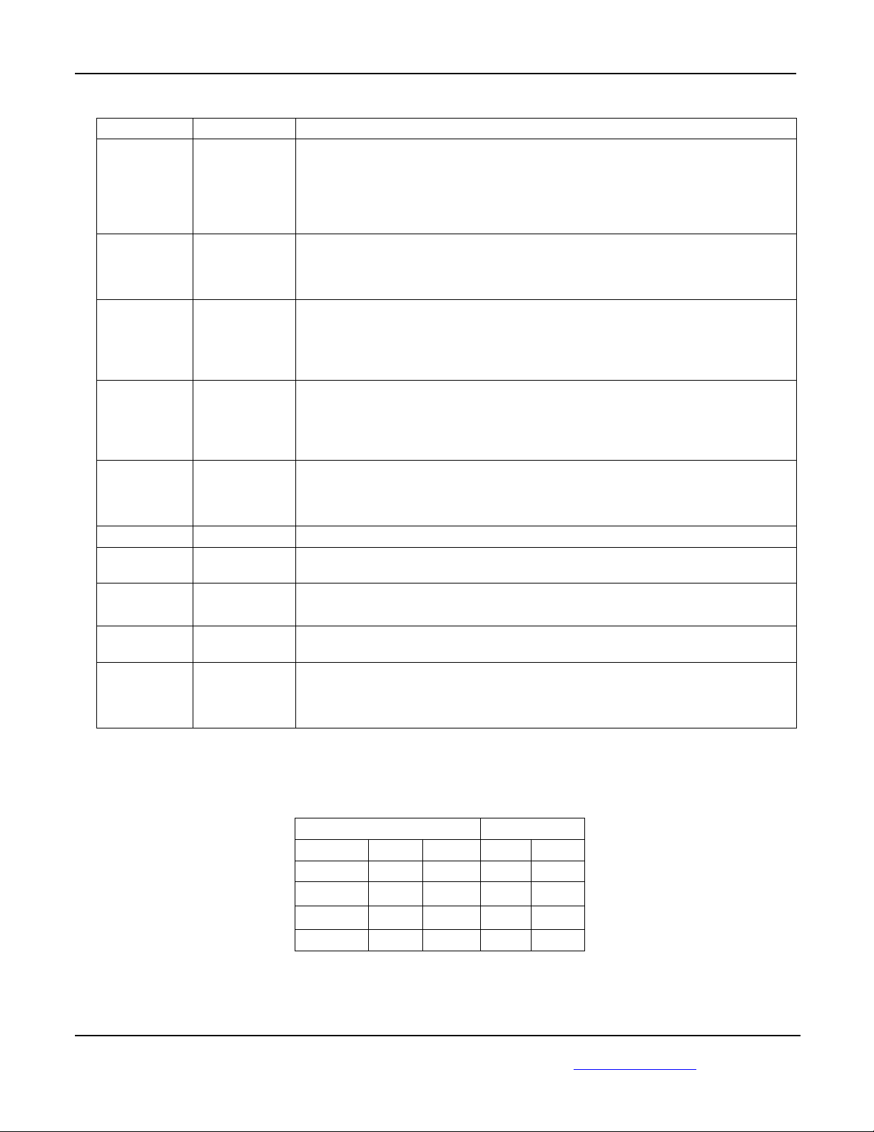
Pin Description
Pin Number Pin Name Pin Function
1, 4 IN, /IN
2 VT
3 VREF-AC
5 EN
6 /MR
7 NC No Connect
8, 13 VCC
12, 9 Q, /Q
10, 11, 14,15
16 DIV_SEL
GND,
Exposed Pad
Differential Input: This input pair is the differential signal input to the device, which
accepts AC- or DC-coupled signal as small as 100mV. The input internally terminates
to a VT pin through 50 and has level shifting resistors of 3.72 k to VCC. This
allows a wide input voltage range from VCC to GND. See Figure 3a, Simplified
Differential Input Stage for details. Note that this input will default to a valid (either
HIGH or LOW) state if left open. See “Input Interface Applications” subsection.
Input Termination Center-Tap: Each side of the differential input pair terminates to
the VT pin. The VT pin provides a center-tap for the input (IN, /IN) to a termination
network for maximum interface flexibility. See “Input Interface Applications”
subsection for more details.
Reference Voltage: This output biases to V
IN and /IN. Connect VREF-AC directly to the VT pin. Bypass with 0.01µF low ESR
capacitor to VCC. Due to limited drive capability, the VREF-AC pin is only intended to
drive its respective VT pin. Maximum sink/source current is ±0.5mA. See “Input
Interface Applications” subsection.
Single-ended Input: This TTL/CMOS-compatible input disables and enables the
output. It is internally connected to a 25k pull-up resistor and will default to a logic
HIGH state if left open. When disabled, Q goes LOW and /Q goes HIGH. EN being
synchronous, outputs will be enabled/disabled after a rising and a falling edge of the
input clock. V
Single-ended Input: This TTL/CMOS-compatible input, when pulled LOW,
asynchronously sets Q output LOW and /Q output HIGH. Note that this input is
internally connected to a 25k pull-up resistor and will default to logic HIGH state if
left open. VTH = VCC/2.
Positive Power Supply: Bypass with 0.1µF in parallel with 0.01µF low ESR capacitors
as close to the V
Differential Output: The LVPECL output swing is typically 800mV and is terminated
with 50 to V
Ground: Ground and exposed pad must be connected to a ground plane that is the
same potential as the ground pins.
Single-ended Input: This TTL/CMOS-compatible input selects divide-by-3 when
pulled LOW and divide-by-5 when pulled HIGH. Note that this input is internally
connected to a 25k pull-up resistor and will default to logic HIGH state if left open.
= VCC/2.
V
TH
= VCC/2.
TH
pins as possible.
CC
-2V. See the “Truth Table” below for the logic function.
CC
–1.2V. It is used for AC-coupling inputs
CC
Truth Table
Inputs Outputs
DIV_SEL EN /MR Q /Q
X X 0 0 1
0 1 1
1 1 1
X 0 1 0 1
August 2007 M9999-080707-A
3
÷
3
÷
5
÷
3
÷
5
or (408) 955-1690
Page 4
Micrel, Inc. SY89228U
Absolute Maximum Ratings
(1)
Operating Ratings
(2)
Supply Voltage (VCC) ..........................–0.5V to +4.0V
Input Voltage (V
LVPECL Output Current (I
) ..................................–0.5V to V
IN
)....................................
OUT
CC
Continuous ................................................. 50mA
Surge........................................................ 100mA
Current (V
Source or sink current on V
)
T
pin…………±100mA
T
Input Current
Supply Voltage (VCC).................. +2.375V to +2.625V
......................................................+3.0V to +3.6V
Ambient Temperature (T
Package Thermal Resistance
®
(θ
®
(ψ
JA
JB
)
)
MLF
Still-Air ..................................................... 75°C/W
MLF
)................ –40°C to +85°C
A
(3)
Junction-to-Board………………………….33°C/W
Source or sink current on (IN, /IN) ........... ±50mA
Current (V
Source/Sink Current on V
REF-AC
)
REF-AC
(4)
............ ±0.5mA
Maximum Operating Junction Temperature…..125°C
Lead Temperature (soldering, 20 sec.) ..........+260°C
Storage Temperature (T
)..................–65°C to 150°C
s
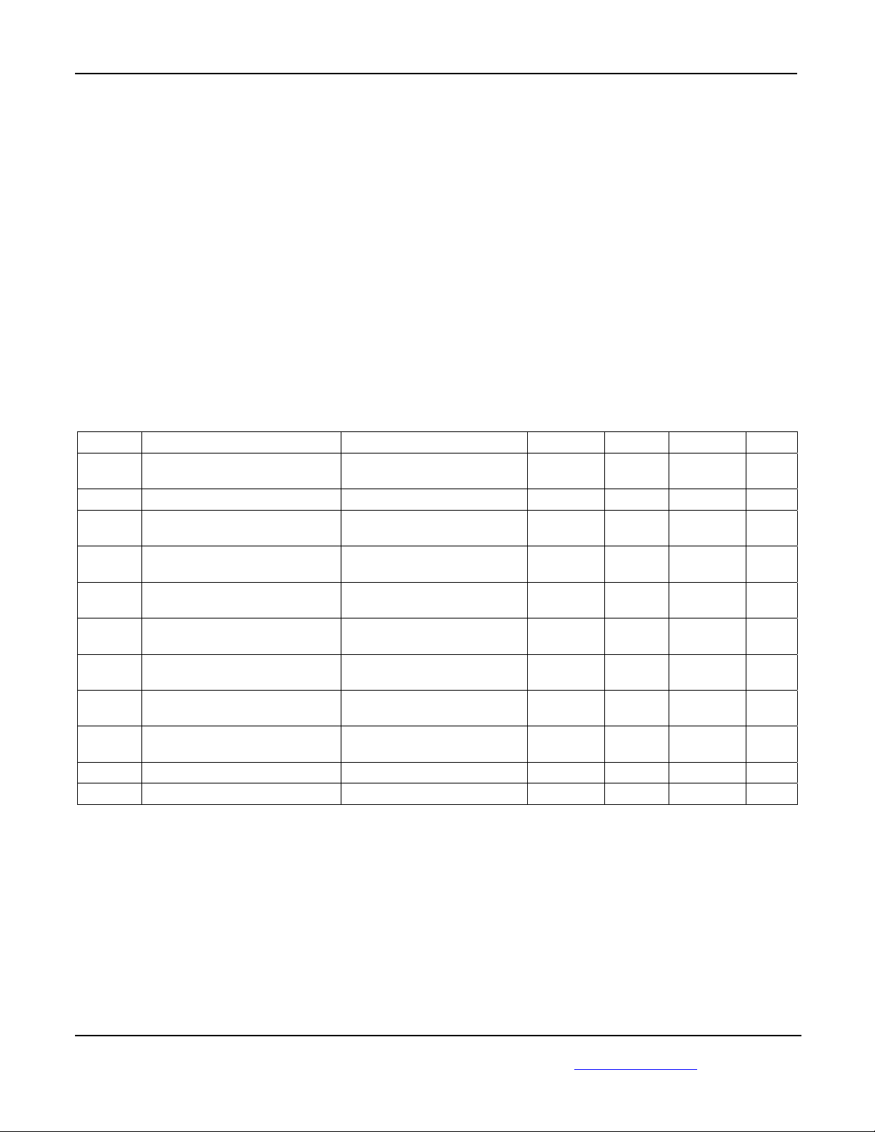
DC Electrical Characteristics
(5)
TA = –40°C to +85°C, unless otherwise stated.
Symbol Parameter Condition Min Typ Max Units
VCC Power Supply
2.375
3.0
ICC Power Supply Current No load, max VCC 40 55 mA
RIN
R
DIFF_IN
Input Resistance
(IN-to-V
Differential Input Resistance
)
T
45 50 55
90 100 110
(IN-to-/IN)
VIH
Input High Voltage
1.2 V
(IN, /IN)
VIL
Input Low Voltage
0 V
(IN, /IN)
VIN
Input Voltage Swing
See Figure 2a. Note 6. 0.1 V
(IN, /IN)
V
DIFF_IN
Differential Input Voltage Swing
See Figure 2b. 0.2 V
|IN-/IN|
V
IN_FSI
Input Voltage Threshold that
30 100 mV
Triggers FSI
V
Output Reference Voltage VCC–1.3 VCC–1.2 VCC–1.1 V
REF-AC
V
Voltage from Input to VT 1.8 V
T_IN
Notes:
1. Permanent device damage may occur if absolute maximum ratings are exceeded. This is a stress rating only and functional operation is
not implied at conditions other than those detailed in the operational sections of this data sheet. Exposure to absolute maximum rating
conditions for extended periods may affect device reliability.
2. The data sheet limits are not guaranteed if the device is operated beyond the operating ratings.
3. Package thermal resistance assumes exposed pad is soldered (or equivalent) to the devices most negative potential on the PCB. θ
values are determined for a 4-layer board in still air unless otherwise stated.
ψ
JB
4. Due to limited drive capability use for input of the same package only.
5. The circuit is designed to meet the DC specifications shown in the above table after thermal equilibrium has been established.
6. V
(max) is specified when V
IN
is floating.
T
2.5
3.3
2.625
3.6
V
CC
–0.1 V
IH
V
CC
JA
V
V
and
August 2007 M9999-080707-A
4
or (408) 955-1690
Page 5
Micrel, Inc. SY89228U
LVPECL Outputs DC Electrical Characteristics
VCC = 2.5V ±5% or 3.3V ±10%; RL = 50 to VCC-2V; TA = –40°C to + 85°C, unless otherwise stated.
Symbol Parameter Condition Min Typ Max Units
VOH
VOL
V
OUT
V
DIFF_OUT
Output HIGH Voltage
Q, /Q
Output LOW Voltage
Q, /Q
Output Voltage Swing
Q, /Q
Differential Output Voltage Swing
Q, /Q
V
V
See Figure 2a. 550 800 950 mV
See Figure 2b. 1100 1600 mV
(7)
-1.145 VCC-0.895 V
CC
-1.945 VCC-1.695 V
CC
LVTTL/CMOS DC Electrical Characteristics
VCC = 2.5V ±5% or 3.3V ±10%; TA = –40°C to + 85°C, unless otherwise stated.
Symbol Parameter Condition Min Typ Max Units
VIH Input HIGH Voltage 2.0 V
VIL Input LOW Voltage 0.8 V
IIH Input HIGH Current -125 30 µA
IIL Input LOW Current -300 µA
Note:
7. The circuit is designed to meet the DC specifications shown in the above table after thermal equilibrium has been established.
(7)
August 2007 M9999-080707-A
5
or (408) 955-1690
Page 6
Micrel, Inc. SY89228U
AC Electrical Characteristics
VCC = 2.5V ±5% or 3.3V ±10%; RL = 50 to VCC-2V; TA = –40°C to + 85°C, unless otherwise stated.
Symbol Parameter Condition Min Typ Max Units
f
MAX
tw Minimum Pulse Width IN, /IN 400 ps
tpd
tRR Reset Recovery Time /MR(L-H)-to-IN 300 ps
tS EN Set-up Time EN-to-IN Note 10 300 ps
tH EN Hold Time IN-to-EN Note 10 800 ps
t
skew
t
JITTER
t
r, tf
Notes:
8. High-frequency AC-parameters are guaranteed by design and characterization.
9. The propagation delay is function of the rise and fall times at IN. Input t
for details.
10. Set-up and hold times apply to synchronous applications that intend to enable/disable before the next clock cycle. For asynchronous
applications, set-up and hold do not apply.
11. Random Jitter is measured with a K28.7 character pattern, measured at <f
12. Cycle-to-Cycle Jitter definition: the variation of periods between adjacent cycles, T
output signal.
13. Total Jitter definition: with an ideal clock input of frequency <f
than the specified peak-to-peak jitter value.
14. For Input Duty Cycle different from 50%, see “Output Duty Cycle Equation” in “Functional Description” subsection.
August 2007 M9999-080707-A
Maximum Input Operating
Frequency
Differential Propagation Delay
In-to-Q
In-to-Q 200mV < V
/MR(H-L)-to-Q 350 570 850 ps
Part-to-Part Skew Note 10
Clock
Random Jitter Note 11 1 ps
Cycle-to-Cycle Jitter Note 12 1 ps
Total Jitter Note 13 10 ps
Output Rise/Fall Time (20% to
80%)
Output Duty Cycle(÷ 3) Duty Cycle(input): 50%; f 1GHz;
Output Duty Cycle(÷ 5)
(8)
V
200mV
OUT
100mV < V
200mV, Note 9 900 1150 1500 ps
IN
800mV, Note 9 800 1050 1400 ps
IN
At full output swing. 100 270 ps
Note 14
Duty Cycle(input): 50%; f 1GHz;
Note 14
/ tf 300ps (20% to 80%). See “Typical Operating Characteristics”
r
.
MAX
– T
where T is the time between rising edges of the
n
n-1
, no more than one output edge in 1012 output edges will deviate by more
MAX
6
1.0 1.5 GHz
450 ps
46 54 %
47 53 %
or (408) 955-1690
RMS
RMS
PP
Page 7

Micrel, Inc. SY89228U
Functional Description
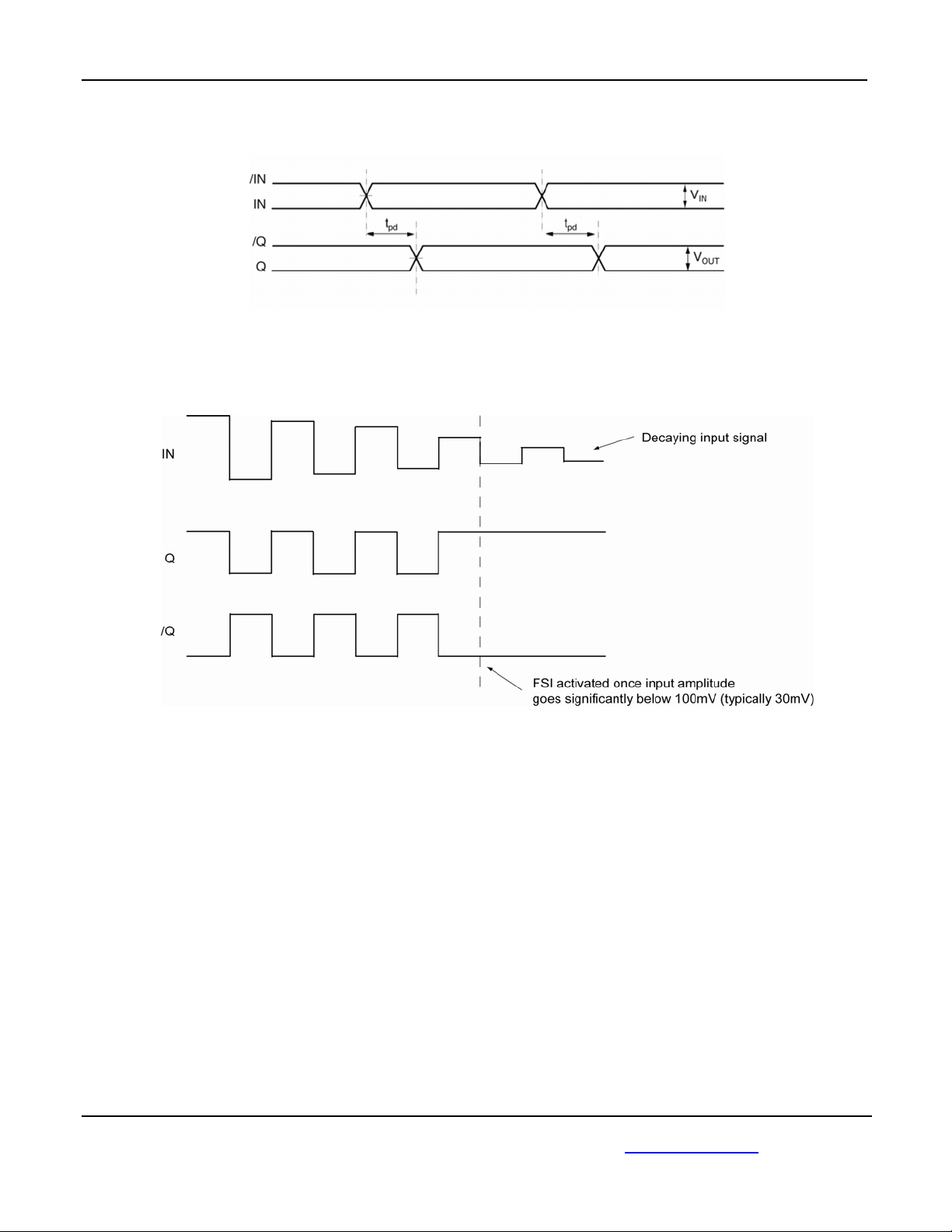
Fail-Safe Input (FSI)
The input includes a special failsafe circuit to sense
the amplitude of the input signal and to latch the
outputs when there is no input signal present, or when
the amplitude of the input signal drops sufficiently
below 100mV
Maximum frequency of the SY89228U is limited by the
FSI function. Refer to Figure 1b.
Input Clock Failure Case
If the input clock fails to a floating, static, or extremely
low signal swing, the FSI function will eliminate a
metastable condition and guarantee a stable output
signal. No ringing and no undetermined state will
occur at the output under these conditions.
Note that the FSI function will not prevent duty cycle
distortion in case of a slowly deteriorating (but still
toggling) input signal as it nears the FSI threshold
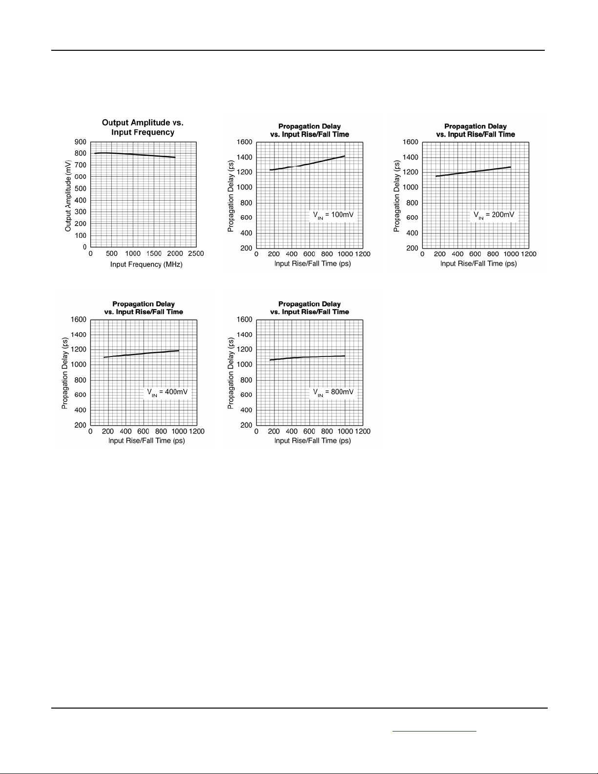
(typically, 30mV). Due to the FSI function, the
propagation delay will depend on rise and fall time of
the input signal and on its amplitude. See “Typical
Operating Characteristics” for detailed information.
Output Duty Cycle Equation
For a non 50% input, derate the spec by:
For Divide by 3:
(0.5 -
For Divide by 5:
(0.5 -
X = input Duty Cycle, in %
Example: if a 45% input duty cycle is applied or X=45,
in divide by 3 mode, the spec would expand by 1.67%
to 44.3%-55.7%
(200mVPP), typically 30mVPK.
PK
X
1
+
100
) x100, in %
3
X
2
+
100
) x100, in %
5
Enable (EN)
EN is a synchronous TTL/CMOS-compatible input that
enables/disables the outputs based on the input to
this pin. Internal 25k pull-up resistor defaults the
input to logic HIGH if left open. Input switching
threshold is V
CC
/2.
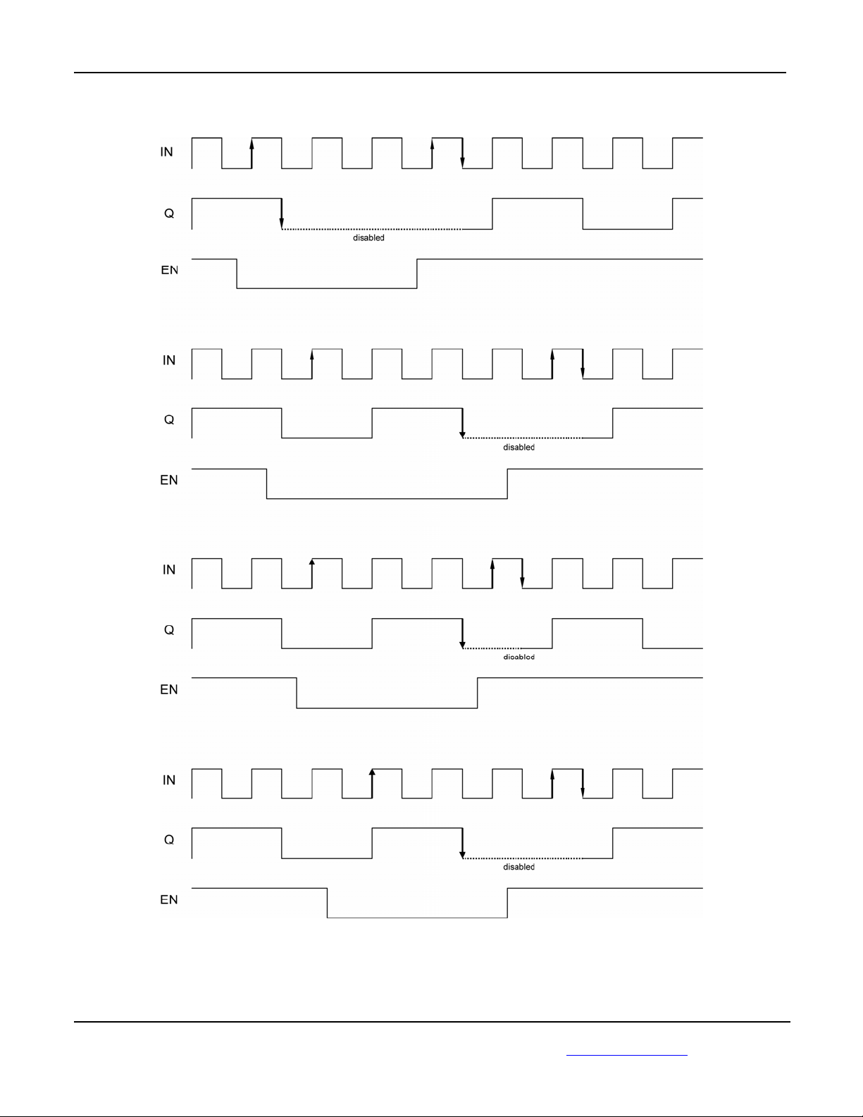
The Enable function operates as follows:
1. The enable/disable function is
synchronous so that the clock outputs will
be enabled or disabled following a rising
and a falling edge of the input clock when
switching from EN = LOW to EN = HIGH.
However, when switching from EN = HIGH
to EN = LOW, the clock outputs will be
disabled following an input clock rising
edge and an output clock falling edge.
2. The enable/disable function always
guarantees the full pulse width at the
output before the clock outputs are
disabled, non-depending on the divider
ratio.
Refer to Figure 1c for examples.
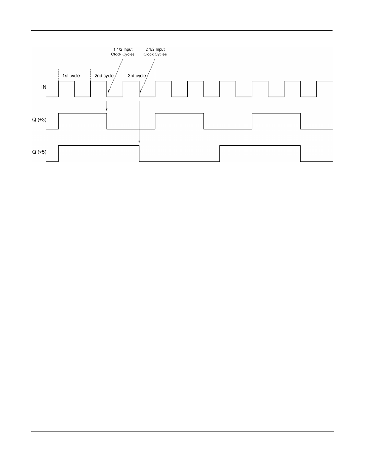
Divider Operation
The divider operation uses both the rising and falling
edge of the input clock. For divide by 3, the falling
edge of the second input clock cycle will determine
the falling edge of the output. For divide by 5, the
falling edge of the third input clock cycle. Refer to
Figure 1d.
August 2007 M9999-080707-A
7
or (408) 955-1690
Page 8
Micrel, Inc. SY89228U
Timing Diagrams
Figure 1a. Propagation Delay
Figure 1b. Fail-Safe Feature
August 2007 M9999-080707-A
8
or (408) 955-1690
Page 9
Micrel, Inc. SY89228U
Figure 1c. Enable Output Timing Diagram Examples (divide by 3)
August 2007 M9999-080707-A
9
or (408) 955-1690
Page 10
Micrel, Inc. SY89228U
Figure 1d. Divider Operation Timing Diagram
August 2007 M9999-080707-A
10
or (408) 955-1690
Page 11
Micrel, Inc. SY89228U
Typical Operating Characteristics
VCC = 3.3V, GND = 0V, VIN = 200mV, tr / tf 300ps, RL = 50 to VCC–2V; TA = 25°C, unless otherwise stated.
August 2007 M9999-080707-A
11
or (408) 955-1690
Page 12
Micrel, Inc. SY89228U
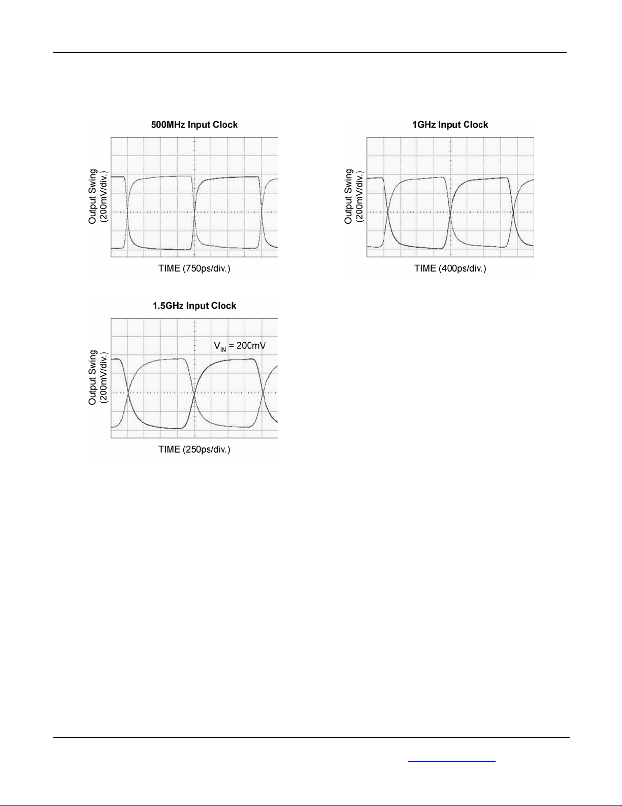
Functional Characteristics
VCC = 3.3V, GND = 0V, VIN = 100mV, Q = Divide by 3, tr/tf 300ps, RL = 50 to VCC-2V; TA = 25°C, unless otherwise stated.
August 2007 M9999-080707-A
12
or (408) 955-1690
Page 13
Micrel, Inc. SY89228U
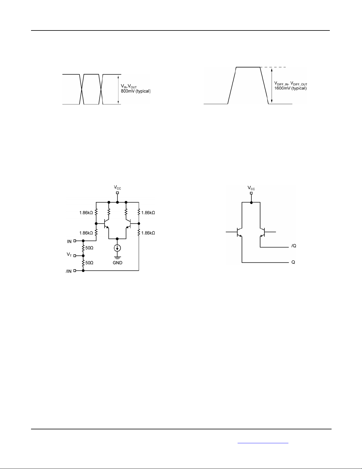
Single-Ended and Differential Swings
Figure 2a. Single-Ended Voltage Swing
Input and Output Stages
Figure 2b. Differential Voltage Swing
Figure 3a. Simplified Differential Input Stage
Figure 3b. Simplified Differential Output Stage
August 2007 M9999-080707-A
13
or (408) 955-1690
Page 14
Micrel, Inc. SY89228U
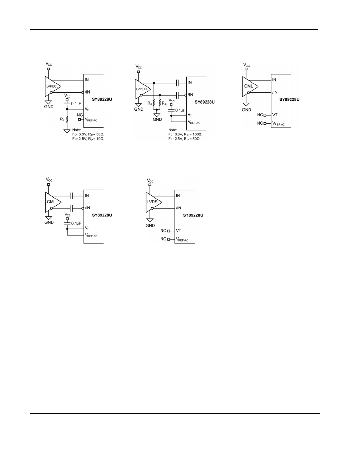
Input Interface Applications
Figure 4a. LVPECL Interface
(DC-Coupled)
Figure 4d. CML Interface
(AC-Coupled)
Figure 4b. LVPECL Interface
(AC-Coupled)
Figure 4e. LVDS Interface
(DC-Coupled)
Option: may connect VT to VCC
Figure 4c. CML Interface
(DC-Coupled)
August 2007 M9999-080707-A
14
or (408) 955-1690
Page 15
Micrel, Inc. SY89228U
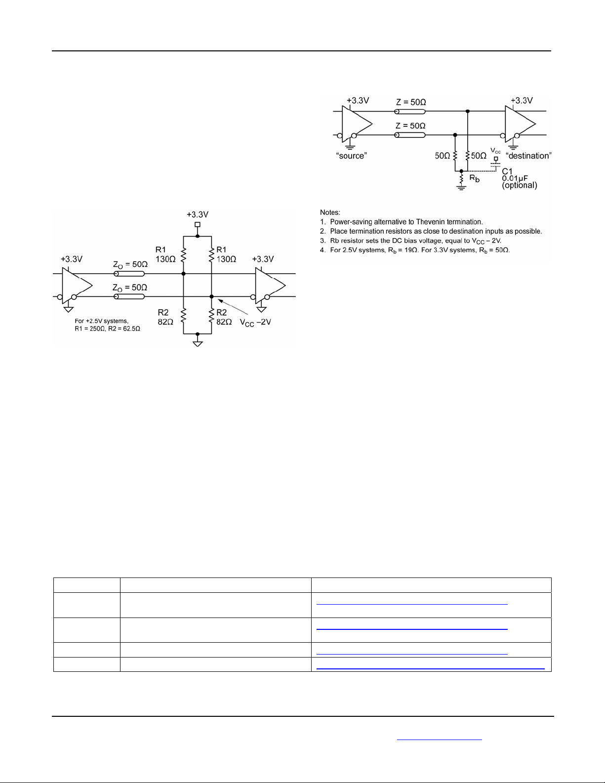
PECL Output Interface Applications
PECL has high input impedance, very low output
impedance (open emitter), and a small signal swing
which results in low EMI. PECL is ideal for driving
50- and 100-controlled impedance transmission
lines. There are several techniques for terminating
the PECL output: parallel termination-thevenin
equivalent, parallel termination (3-resistor), and ACcoupled termination. Unused output pairs may be
left
floating. However, single-ended outputs must
be terminated, or balanced.
Figure 5b. Parallel Termination
(3-Resistor)
Figure 5a. Parallel Termination-Thevenin
Equivalent
Related Product and Support Documentation
Part Number Function Datasheet Link
SY89229U
SY89230U
SY89231U
MLF® Application Note www.amkor.com/products/notes_papers/MLFAppNote.pdf
1GHz Precision, LVDS ÷3, ÷5 Clock Divider
with Fail Safe Input and Internal Termination
3.2GHz Precision, LVPECL ÷3, ÷5 Clock
Divider
3.2GHz Precision, LVDS ÷3, ÷5 Clock Divider
http://www.micrel.com/_PDF/HBW/sy89229u.pdf
http://www.micrel.com/_PDF/HBW/sy89230u.pdf
http://www.micrel.com/_PDF/HBW/sy89231u.pdf
August 2007 M9999-080707-A
15
or (408) 955-1690
Page 16
Micrel, Inc. SY89228U
r
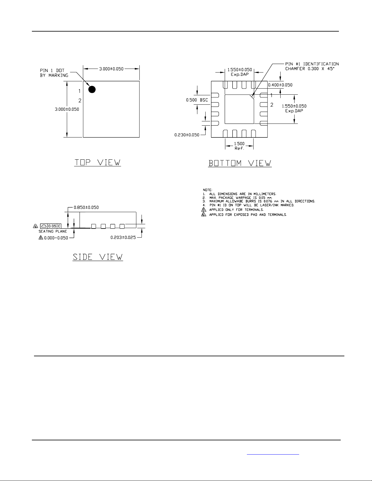
Package Information
16-Pin MicroLeadFrame® (MLF-16)
Packages Notes:
1. Package meets Level 2 Moisture Sensitivity Classification.
2. All parts are dry-packed before shipment.
3. Exposed pad must be soldered to a ground for proper thermal management.
The information furnished by Micrel in this data sheet is believed to be accurate and reliable. However, no responsibility is assumed by Micrel for
its use. Micrel reserves the right to change circuitry and specifications at any time without notification to the customer.
Micrel Products are not designed or authorized for use as components in life support appliances, devices or systems where malfunction of a
product can reasonably be expected to result in personal injury. Life support devices or systems are devices or systems that (a) are intended fo
surgical implant into the body or (b) support or sustain life, and whose failure to perform can be reasonably expected to result in a significant
injury to the user. A Purchaser’s use or sale of Micrel Products for use in life support appliances, devices or systems is a Purchaser’s own risk
and Purchaser agrees to fully indemnify Micrel for any damages resulting from such use or sale.
MICREL, INC. 2180 FORTUNE DRIVE SAN JOSE, CA 95131 USA
TEL +1 (408) 944-0800 FAX +1 (408) 474-1000 WEB http:/www.micrel.com
© 2007 Micrel, Inc.
August 2007 M9999-080707-A
16
or (408) 955-1690
 Loading...