

Page 1

OC-3/STS-3
C
CLOCK RECOVERING
TRANSCEIVER
SY69952A
FEATURES
■ A complete SONET/SDH/ATM compatible single chip
Transmitter and Receiver
■ Seamless operation with PMC-Sierra PM5345, VLSI
VNS67200, Ig
µPD98402 UNI Processors
■ Supports clock and data recovery from 51.84 Mbit/s
or 155.52 Mbit/s NRZ or NRZI data stream
■ 155.52MHz clock multiplication from 19.44MHz
source or 51.84MHz clock multiplication from
6.48MHz source
■ Line Receiver Inputs: No external buffering needed
■ Differential output buffering
■ Link Status Indication
■ Loop-back testing
■ 100K ECL compatible I/O
■ Single +5 volt power supply
■ Available in 28-pin SOIC package
T WAC-013-B/WAC-413-A and
NEC
DESCRIPTION
Micrel-Synergy's SY69952A contains fully integrated
transmitter and receiver functions designed to provide
clock recovery and generation for either 51.84Mbit/s OC/
STS-1 or 155.52Mbit/s OC/STS-3 SONET/SDH
(SY69952) and ATM applications.
On-chip clock generation is performed by a low-jitter
phase-locked loop (PLL) allowing use of 19.44MHz
reference for 155.52MHz generation or a 6.48MHz
reference for 51.84MHz generation. Clock recovery is
performed by synchronizing the on-chip VCO directly to
the incoming data stream.
Micrel-Synergy's circuit design techniques coupled with
ASSET™ bipolar technology result in ultra-fast
performance with low noise and low power dissipation.
FUNCTIONAL BLOCK DIAGRAM
PLL2+
PLL2-
PLL
PLL
x8
PLL1+
PLL1-
RECEIVE
TRANSMIT
ROUT+
ROUT-
RIN+
RIN-
CD
TOUT+
TOUT-
LOOP MODE
REFCLK+
REFCLK-
RCLK+
RCLK-
RSER+
RSER-
LFI
TSER+
TSER-
TCLK+
TCLK-
PIN CONFIGURATION
ROUT+
ROUT-
RIN+
RIN-
MODE
V
C
CD
LOOP
REFCLK-
REFCLK+
TOUT-
TOUT+
PLL1+
PLL1- PLL2-
1
2
3
4
5
6
7
8
9
10
11
12
13
14
TOP VIEW
SOIC
28
27
26
25
24
23
22
21
20
19
18
17
16
15
RCLKRCLK+
RSERRSER+
LFI
V
CC
V
EE
V
CC
TCLKTCLK+
TSER+
TSERPLL2+
Rev.: C Amendment: /0
1
Issue Date: May 2000
Page 2

Micrel
PIN DESCRIPTIONS
SY69952A
INPUTS
± – Differential PECL Input
RIN
Receive Input. These built-in line receiver inputs are
connected to the differential Receive serial input data stream.
An internal Receive PLL recovers the embedded clock
(RCLK±) and data (RSER±) information. The incoming data
rate can be within one of two frequency ranges, mentioned
before depending on the state of the MODE pin.
CD – PECL/TTL Input
Carrier Detect. This input controls the recovery function
of the Receive PLL and can be driven by the carrier detect
output from optical modules or from external transition
detection circuitry. When this input is at an ECL HIGH, the
input data stream (RIN±) is recovered normally by the
Receive PLL. When this input is at an ECL LOW, the
Receive PLL no longer aligns to RIN±, but instead aligns
with the REFCLK × 8 frequency. Also, the Link Fault Indicator
(/LFI) will transition LOW, and the recovered data outputs
(RSER±) will remain LOW regardless of the signal level on
the Receive data stream inputs (RIN±). When the CD input
is at a TTL LOW (≤0.8V), the internal transition detection
circuitry is disabled. When in Loop-back testing mode,
regardless of the signal level on the CD input, the Receive
PLL is internally turned-on to allow data stream transmission
to the recovered serial data outputs (RSER±) from the
Transmit serial data inputs (TSER±).
TSER
± – Differential PECL Input
Transmit Serial Data. These built-in line receiver inputs
are connected to the differential Transmit serial input data
stream. These inputs can receive very low amplitude signals
and are compatible with PECL signal levels.
REFCLK± – Differential PECL/TTL Input
Reference Clock. This input is the clock frequency
reference for the clock and data recovery Receive PLL.
REFCLK is multiplied internally by eight and sets the
approximate center frequency for the internal Receive PLL
to track the incoming bit stream. This input is also multiplied
by eight by the frequency multiplier Transmit PLL to produce
the bit rate Transmit Clock (TCLK±). REFCLK can be
connected to either a differential PECL or single-ended TTL
frequency source. When either REFCLK+ or REFCLK- is at
a TTL LOW, the opposite REFCLK signal becomes a TTL
level input.
OUTPUTS
ROUT± – Differential PECL Output
Receive Output. These Positive ECL 100K outputs (+5V
referenced) represent the buffered version of the input data
stream (RIN±). This output pair can be used for Receiver
input data equalization in copper based systems, reducing
the system impact of data dependent jitter. All PECL outputs
can be powered down by connecting both outputs to VCC
or leaving them both unconnected.
± – Differential PECL Output
RSER
Recovered Serial Data. These Positive ECL 100K outputs
(+5V referenced) represent the recovered data from the
input data stream (RIN±). This recovered data is aligned
with the recovered clock (RCLK±) with a sampling window
compatible with most data processing devices.
RCLK± – Differential PECL Output
Recovered Clock. These Positive ECL 100K outputs (+5V
referenced) represent the recovered clock from the input
data stream (RIN±). This recovered clock is used to sample
the recovered data (RSER±) and has timing compatible
with most data processing devices.
/LFI – TTL Output
Link Fault Indicator. This output indicates the status of
the input data stream (RIN±). It is controlled by three
functions; the Carrier Detect (CD) input, the internal
Transition Detector, and the Out of Lock (OOL) detector.
The Transition Detector determines if RIN± contains enough
transitions to be accurately recovered by the Receive PLL.
The Out of Lock detector determines if RIN± is within the
frequency range of the Receive PLL. When CD is HIGH
and RIN± has sufficient transitions and is within the
frequency range of the Receive PLL, the /LFI output will be
high. If CD is at an ECL LOW or RIN± does not contain
sufficient transitions or RIN± is outside the frequency range
of the Receive PLL then the /LFI output will be LOW. If CD
is at a TTL LOW then the /LFI output will only transition
LOW when the frequency of RIN± is outside the range of
the Receive PLL.
TOUT
± – Differential PECL Output
Transmit Output. These Positive ECL 100K outputs (+5V
referenced) represent the buffered version of the Transmit
data stream (TSER±). This Transmit path is used to take
weak input signals and rebuffer them to drive low impedance
copper media.
TCLK± – Differential PECL Output
Transmit Clock. These Positive ECL 100K outputs (+5V
referenced) provide the bit rate frequency source for external
Transmit data processing devices. This output is synthesized
by the Transmit PLL and is derived by multiplying the
REFCLK frequency by eight.
2
Page 3
Micrel
Transmit
Filter
PIN DESCRIPTIONS
SY69952A
/LOOP – TTL Input
Loop Back Select. This input is used to select the input
data stream source that the Receive PLL uses for clock
and data recovery. When the /LOOP input is HIGH, the
Receive input data stream (RIN±) is used for clock and
data recovery. When /LOOP is LOW, the Transmit input
data stream (TSER±) is used by the Receive PLL for clock
and data recovery. When in Loop-back testing mode, /LOOP
input asserted low, the Receive PLL is always turned-on
internally regardless of the CD input signal level status.
This allows the Recovered Serial Data outputs (RSER±) to
receive data stream from the Transmit serial data inputs
(TSER±).
MODE – 3 Level Input
Frequency Mode Select. This three-level input selects
the frequency range for the clock and data recovery receive
PLL and the frequency multiplier transmit PLL. When the
input is held PECL HIGH (VCC –0.9 typ.), the two PLLs
operate at the SONET (SDH) STS-3 (STM-1) line rate of
155.52MHz. When this input is held TTL LOW (connected
to GND), the two PLLs operate at one SONET STS-1 line
rate of 51.84MHz. The REFCLK± frequency in both operating
modes is 1⁄8 of the operating frequency. When the MODE
input is ECL LOW (VCC – 1.7 typ), the device enters into
test mode, the TSER± inputs substitue for the internal PLL
VCO for use in factory testing.
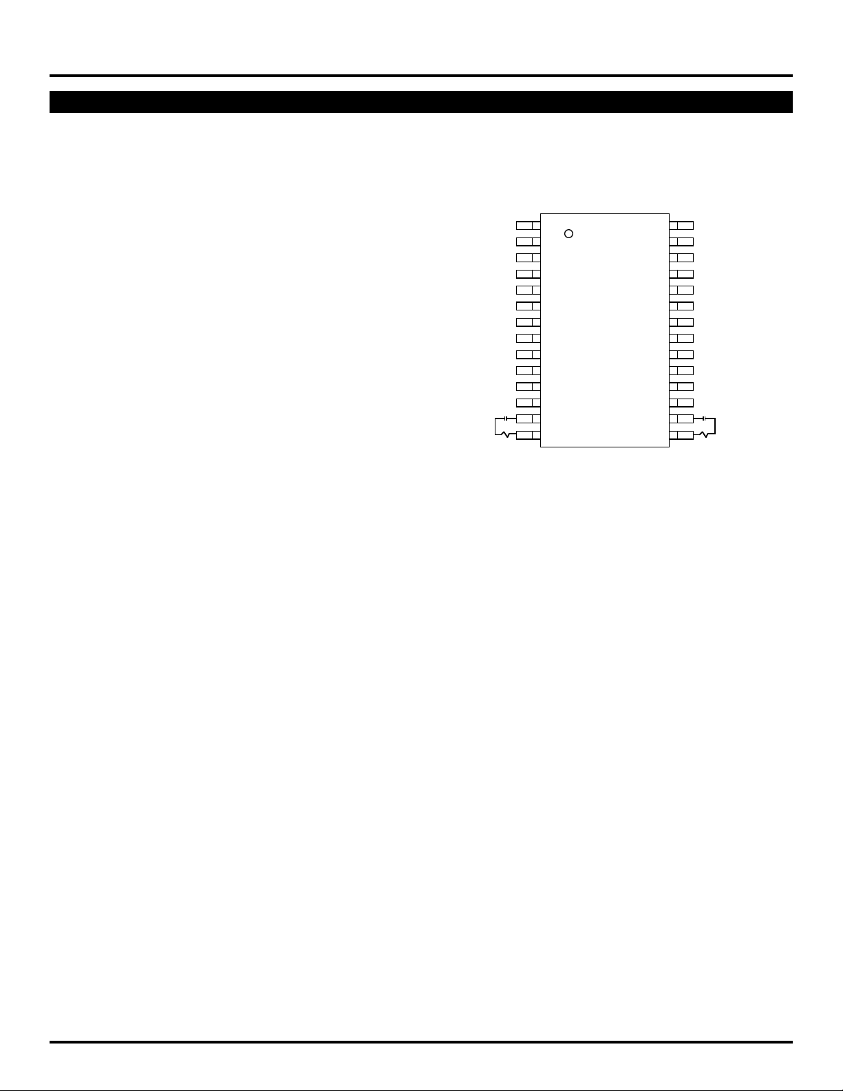
PLL1±, PLL2± – Loop Filter Inputs
These pins are used to connect the external loop filters
for the two on-board PLLs. See below:
TOP VIEW
0.1µf
500Ω
Figure 1. Suggested Loop Filter Values
PLL1+
PLL1- PLL2-
PLL2+
0.1µf
120Ω
Receiver
Filter
3
Page 4

Micrel
DESCRIPTION
SY69952A
General
The SY69952A Transceiver is used in SONET/SDH and
ATM applications to recover clock and data information from
a 155.52MHz or 51.84MHz NRZ (Non Return to Zero) or
NRZI (Non Return to Zero Invert on ones) serial data stream.
This device also provides a bit-rate Transmit clock, from a
byte rate source through the use of a frequency multiplier
PLL, and differential data buffering for the Transmit side of
the system. This device is compliant with all relevant SONET/
SDH specifications including ANSI T1X1.6/91-022, ANSI
T1X1.3/93-006R1 Draft and ITU/CCITT G958.
Operating Frequency
The SY69952A operates at either of two frequency
ranges, the MODE input determines with which of the two
frequencies 51.84MHz or 155.52MHz the Transmit frequency
multiplier PLL, the Receive clock and the data recovery
PLL will operate. When MODE is connected to VCC, the
highest operating range of the device is selected. A
19.44MHz ±1% source must drive the REFCLK input and
the two PLLs will multiply this rate by 8 to provide output
clocks that operate at 155.52MHz ±1%. When the MODE
input is connected to ground (GND), the lowest operating
range of the device is selected. A 6.48MHz ±1% source
must drive the REFCLK inputs and the two PLLs will multiply
this rate by 8 to provide output clocks that operate at
51.84MHz ±1%.
Transmit Functions
The transmit section of the SY69952A contains a PLL
that takes a REFCLK input and multiplies it by 8 (REFCLKx8)
to produce a PECL (Positive ECL) differential output clock
(TCLK±). The transmitter has two operating ranges that are
selectable with the three-level MODE pin as explained above.
The SY69952A Transmit frequency multiplier PLL allows
low-cost byte rate clock sources to be used to time the
upstream serial data transmitter.
The REFCLK± inputs can be configured three ways.
When both REFCLK+ and REFCLK– are connected to a
differential 100K-compatible PECL source, the REFCLK±
inputs will behave as a differential PECL inputs. When either
the REFCLK+ or the REFCLK– input is at a TTL LOW, the
other REFCLK input becomes a TTL–level input allowing it
to be connected to a low-cost TTL crystal oscillator. The
REFCLK± inputs structure, therefore, can be used as a
differential PECL input, a single TTL input, or as a dual TTL
clock multiplexing input.
The Transmit PECL differential input pair (TSER±) is
buffered by the SY69952A yielding the differential data
outputs (TOUT±). These outputs can be used to directly
drive transmission media such as Printed Circuit Board
(PCB) traces, optical drivers, twisted pair, or coaxial cable.
Receive Functions
The primary function of the receiver is to recover clock
(RCLK±) and data (RSER±) from the incoming differential
PECL data stream (RIN±) without the need for external
buffering. These built-in line receiver inputs, as well as the
TSER± inputs mentioned above, have a wide commonmode range (2.5V) and the ability to receive signals with as
little as 50mV differential voltage. They are compatible with
all PECL signals and any copper media.
The clock recovery function is performed using an
embedded PLL. The recovered clock is not only passed to
the RCLK± outputs, but also used internally to sample the
input serial stream in order to recover the data pattern. The
Receive PLL uses the REFCLK input as a byte-rate
reference. This input is multiplied by 8 (REFCLK × 8) and is
used to improve PLL lock time and to provide a center
frequency for operation in the absence of input data stream
transitions. The receiver can recover clock and data in two
different frequency ranges depending on the state of the
MODE pin as explained earlier. To insure accurate data
and clock recovery, REFCLK × 8 must be within 1000ppm
of the transmit bit rate. The standards, however, specify
that the REFCLK × 8 frequency accuracy be within 20100ppm.
The differential input serial data (RIN±) is not only used
by the PLL to recover the clock and data, but it is also
buffered and presented as the PECL differential output pair
ROUT±. This output pair can be used as part of the
transmission line interface circuit for base line wander
compensation, improving system performance by providing
reduced input jitter and increased data eye opening.
Carrier Detect and Link Fault Indicator Functions
The Link Fault Indicator (/LFI) output is a TTL–level output
that indicates the status of the receiver. This output can be
used by an external controller for Loss of Signal (LOS),
Loss of Frame (LOF), or Out of Frame (OOF) indications.
/LFI is controlled by the Carrier Detect input, the internal
Transitions Detector, and the PLL Out of Lock (OOL)
circuitry.
The CD input may be driven by external circuitry that is
monitoring the incoming data stream. Optical modules have
CD outputs that indicate the presence of light on the optical
fiber and some copper based systems use external threshold
detection circuitry to monitor the incoming data stream. The
CD input is a 100K PECL compatible signal that should be
held HIGH when the incoming data stream is valid. When
CD is pulled to a PECL LOW (≤2.5V max.), the /LFI output
will transition LOW except in the loopback mode, and the
Receiver PLL will align itself with the REFCLKx8 frequency
and the recovered data outputs (RSER±) will remain LOW
regardless of the signal level on the Receive data-stream
inputs (RIN±).
4
Page 5

Micrel
DESCRIPTION
SY69952A
In addition, the SY69952A has a built-in transitions
detector that also checks the quality of the incoming data
stream. The absence of data transitions can be caused by
a broken transmission media, a broken transmitter, or a
problem with the transmit or receive media coupling. The
SY69952A will detect a quiet link by counting the number of
bits time that have passed without a data transition. A bit
time is defined as the period of RCLK±. When 512 bit times
have passed without a data transition on RIN±, /LFI will
transition LOW. The receiver will assume that the serial
data stream is invalid and, instead of allowing the RCLK±
frequency to wander in the absence of data, the PLL will
lock to the REFCLK × 8 frequency. This will insure that
RCLK± is as close to the correct link operating frequency
as the REFCLK± accuracy. /LFI will be driven HIGH again
and the receiver will recover clock and data from the
incoming data stream when the transition detection circuitry
determines that adequate transitions to ensure reliable clock
and data recovery have been detected within 512 bit-times.
The Transition Detector can be turned off by pulling the
CD input to a TTL LOW (≤0.8V). When CD is pulled to a
TTL LOW the /LFI will only be driven LOW if the recovered
clock is not locked to the incoming data stream. LFI LOW in
this will only indicate that the Receiver PLL is Out of Lock
(OOL). The CD pin should not be left unconnected.
Loop Back Testing
The TTL level /LOOP pin is used to perform loop-back
testing. When /LOOP is asserted (held LOW) the Transmitter
serial input (TSER±) is used by the Receiver PLL for clock
and data recovery. This allows in-system testing to be
performed on the entire device except for the differential
Transmit drivers (TOUT±) and the differential Receiver inputs
(RIN±). For example, an ATM controller can present ATM
cells to the input of the ATM cell processor and check to
see that these same cells are received. When the /LOOP
input is deasserted (held HIGH) the Receive PLL is once
again connected to the Receiver serial inputs (RIN±).
The /LOOP feature can also be used in applications where
clock and data recovery are to be performed from either of
two data streams. In these systems the /LOOP pin is used
to select whether the TSER± or the RIN± inputs are used
by the Receive PLL for clock and data recovery. In the
Loop back testing mode, regardless of the CD signal status
and the presence of data at the input (RIN±), the transmit
serial data stream from (TSER±) will flow through the
Receive PLL to the Recovered serial data output (RSER±).
5
Page 6
Micrel
SY69952A
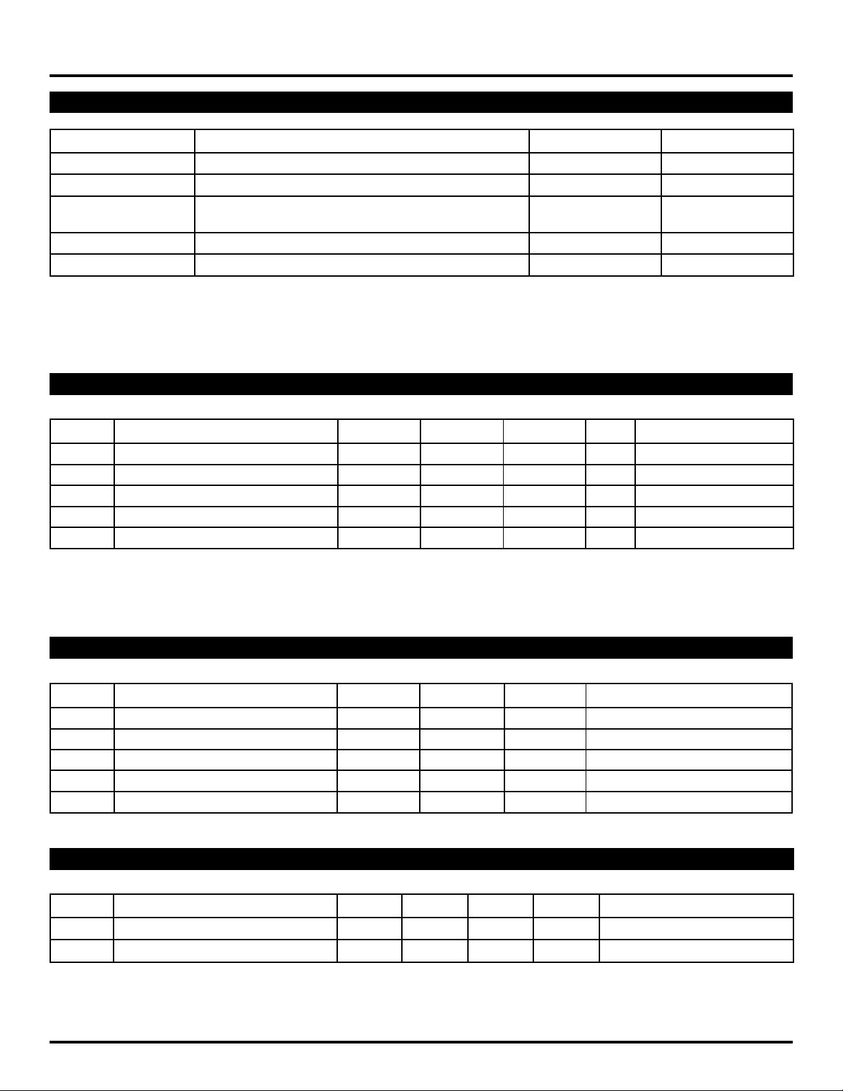
ABSOLUTE MAXIMUM RATINGS
(1)
Symbol Parameter Rating Unit
VCC, TVCC, AV
V
I
I
OUT
T
A
T
store
NOTE:
1. Permanent device damage may occur if ABSOLUTE MAXIMUM RATINGS are exceeded. This is a stress rating only and functional operation is not implied
at conditions other than those detailed in the operational sections of this data sheet. Exposure to ABSOLUTE MAXIMUM RATING conditions for extended
periods may affect device reliability.
CC
Power Supply (GND, TGND, AGND = 0V) 0 to +7 V
Input Voltage (GND, TGND, AGND = 0V) 0 to V
CC
V
Output Current –Continuous 50 mA
–Surge 100
Ambient Temperature Range 0 to +85 °C
Storage Temperature Range –65 to +150 °C
PECL DC ELECTRICAL CHARACTERISTICS
VCC = TVCC = AVCC = 4.75V to 5.25V; GND, TGND, AGND = 0V, TA = 0°C to +85°C
Symbol Parameter Min. Typ. Max. Unit
V
OH
V
OL
V
IH
V
IL
I
IL
NOTES:
1. Equilibrium temperature
2. Forcing one input at a time. Apply VIH(max) or VIL(min) to all other inputs.
Output HIGH Voltage VCC –1.075 VCC –.955 VCC –.830 V
Output LOW Voltage VCC –1.860 VCC –1.705 VCC –1.570 V
(2)
(2)
VCC –1.165 — VCC –.880 V
VCC –1.810 — VCC –1.475 V
Input HIGH Voltage
Input LOW Voltage
Input LOW Current 0.5 ——µA
(1)
TTL DC ELECTRICAL CHARACTERISTICS
VCC = TVCC = AVCC = 4.75V to 5.25V; GND, TGND, AGND = 0V, TA = 0°C to +85°C
Symbol Parameter Min. Max. Unit Condition
V
OH
V
OL
I
OS
V
IH
V
IL
DC ELECTRICAL CHARACTERISTICS — TTL
DC ELECTRICAL CHARACTERISTICS
VCC = +5V ±5%; VEE = GND = 0V, TA = 0°C to +85°C
Symbol Parameter Min. Typ. Max. Unit Condition
I
EE
I
OUT
NOTES:
1. To calculate total power supply current into the VCC pins: ICC = (n * I
2. To calculate total device power dissipation; PD = [IEE * (VCC – VEE)] + [n * I
3. Average ECL output voltage is calculated as V
Output HIGH Voltage 2.4 — VI
= –2mA
OH
Output LOW Voltage — 0.45 V IOL = 4mA
Output Short Circuit Current –150 –60 mA V
OUT
= 0V
Input HIGH Voltage 2.0 — V —
Input LOW Voltage — 0.8 V —
(1), (2), (3)
Internal Operating Current — 140 200 mA
Termination Output Current — 11 — mA 50Ω to VCC –2, 50% duty cycle
); where n = number of ECL output pins used (ie, terminated).
OUT
= (VOH(max) + VOH(min) + VOL(max) + VOL(min)) /4 = 1.33V.
OAVG
OUT
* 1.33]
(3)
.
6
Page 7
Micrel
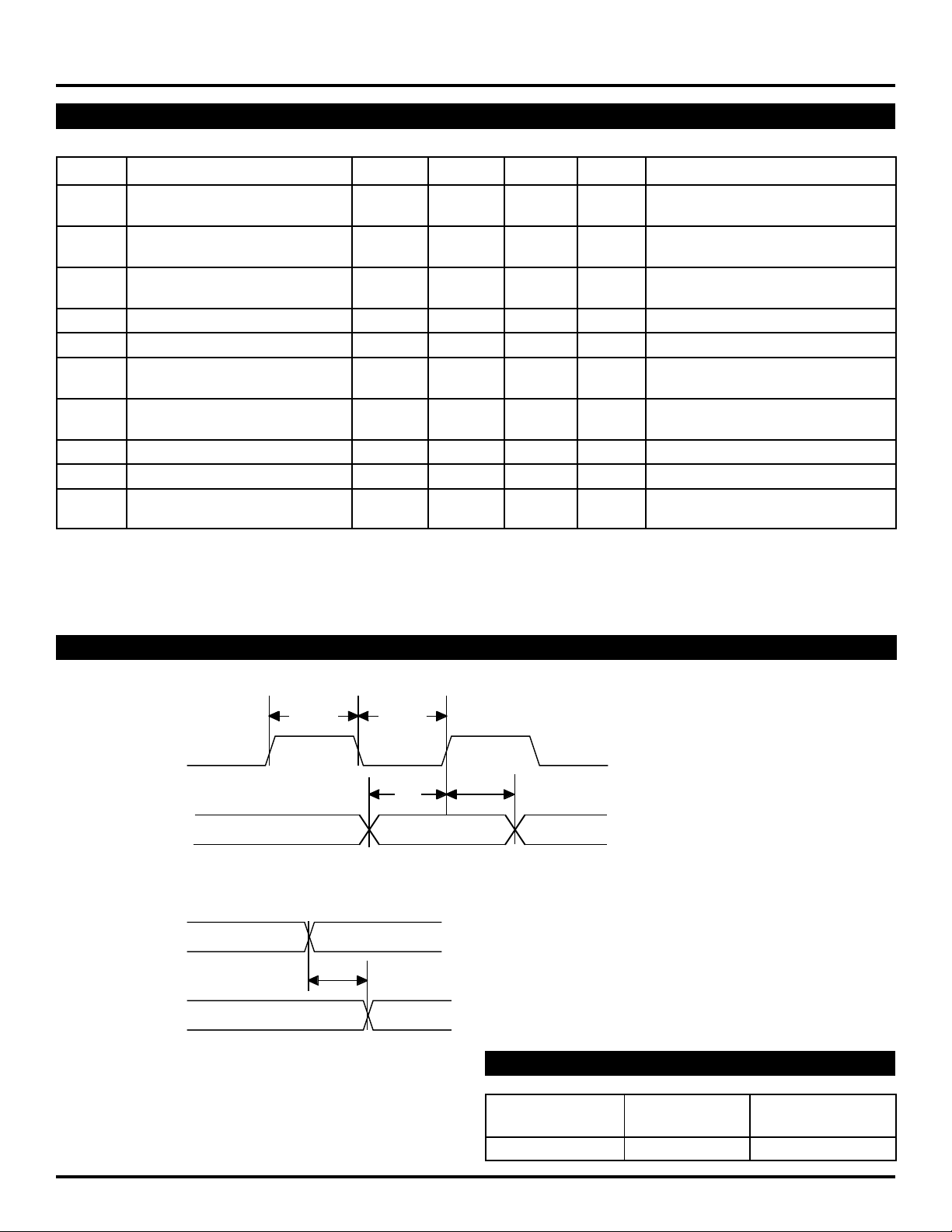
AC ELECTRICAL CHARACTERISTICS
VCC = +5V ±5%; VEE = GND = 0V, TA = 0°C to +85°C
Symbol Parameter Min. Typ. Max. Units Condition
f
REF
f
B
t
ODC
t
RF
t
LOCK
t
RPWH
t
RPWL
t
DV
t
DH
t
PD
NOTES:
1. fB is calculated as 1/(f
2. Tested initially and after any design or process changes that may affect these parameters.
3. The ECL switching threshold is the differential zero crossing (ie, the point where + and – signals cross).
Reference Frequency 6.41 6.48 6.55 MHz MODE = 0
19.24 19.44 19.64 MHZ MODE = 1
Bit Time
(1)
19.5 19.3 19.1 ns MODE = 0
6.50 6.43 6.36 ns MODE = 1
Output Duty Cycle
(2)
48 — 52 %
(TCLK±, RCLK±)
ECL Output Rise/Fall Tiime
(2)
0.4 — 1.2 ns 5pf load, 50Ω to VCC –2 (20% to 80%)
PLL Lock Time —— 1 µs RIN transition density 25%
REFCLK Pulse Width High 3.3 ——ns MODE = 0
10 ——ns MODE = 1
REFCLK Pulse Width Low 3.3 ——ns MODE = 0
10 ——ns MODE = 1
Data Valid 3 ——ns Prior to RCLK+ rising edge
Data Hold 1 ——ns After RCLK+ rising edge
Propagation Delay
(3)
——10 ns MODE = 1
(RIN to ROUT, TSER to TOUT)
* 8).
REF
SY69952A
TIMING WAVEFORMS
RCLKP
RSERP/RSERN
TSERP/TSERN
RINP/RINN
ROUTP/ROUTN
t
ODC
t
ODC
t
t
DV
t
PD
DH
PRODUCT ORDERING CODE
Ordering Package Operating
Code Type Range
SY69952AZC Z28-1 Commercial
7
Page 8
Micrel
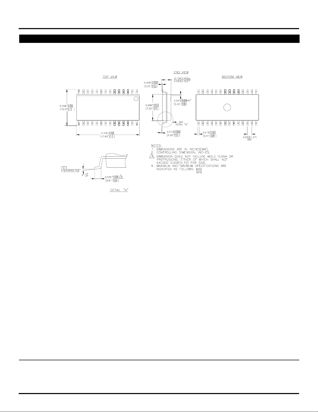
28 LEAD SOIC .300" WIDE (Z28-1)
SY69952A
Rev. 02
MICREL-SYNERGY 3250 SCOTT BOULEVARD SANTA CLARA CA 95054 USA
TEL + 1 (408) 980-9191 FAX + 1 (408) 914-7878 WEB http://www.micrel.com
This information is believed to be accurate and reliable, however no responsibility is assumed by Micrel for its use nor for any infringement of patents or
other rights of third parties resulting from its use. No license is granted by implication or otherwise under any patent or patent right of Micrel Inc.
© 2000 Micrel Incorporated
8
 Loading...