

Page 1
3.3V 1:22 HIGH-PERFORMANCE,
LO W VOL T A GE
BUS CLOCK DRIVER
ClockWorks™
SY89824L
FEATURES
■ 3.3V core supply, 1.8V output supply for reduced
power
■ LVPECL and HSTL inputs
■ 22 differential HSTL (low-voltage swing) output pairs
■ HSTL outputs drive 50Ω to ground with no offset
voltage
■ Low part-to-part skew (200ps max.)
■ Low pin-to-pin skew (50ps max.)
■ Available in a 64-Pin EPAD HQFP
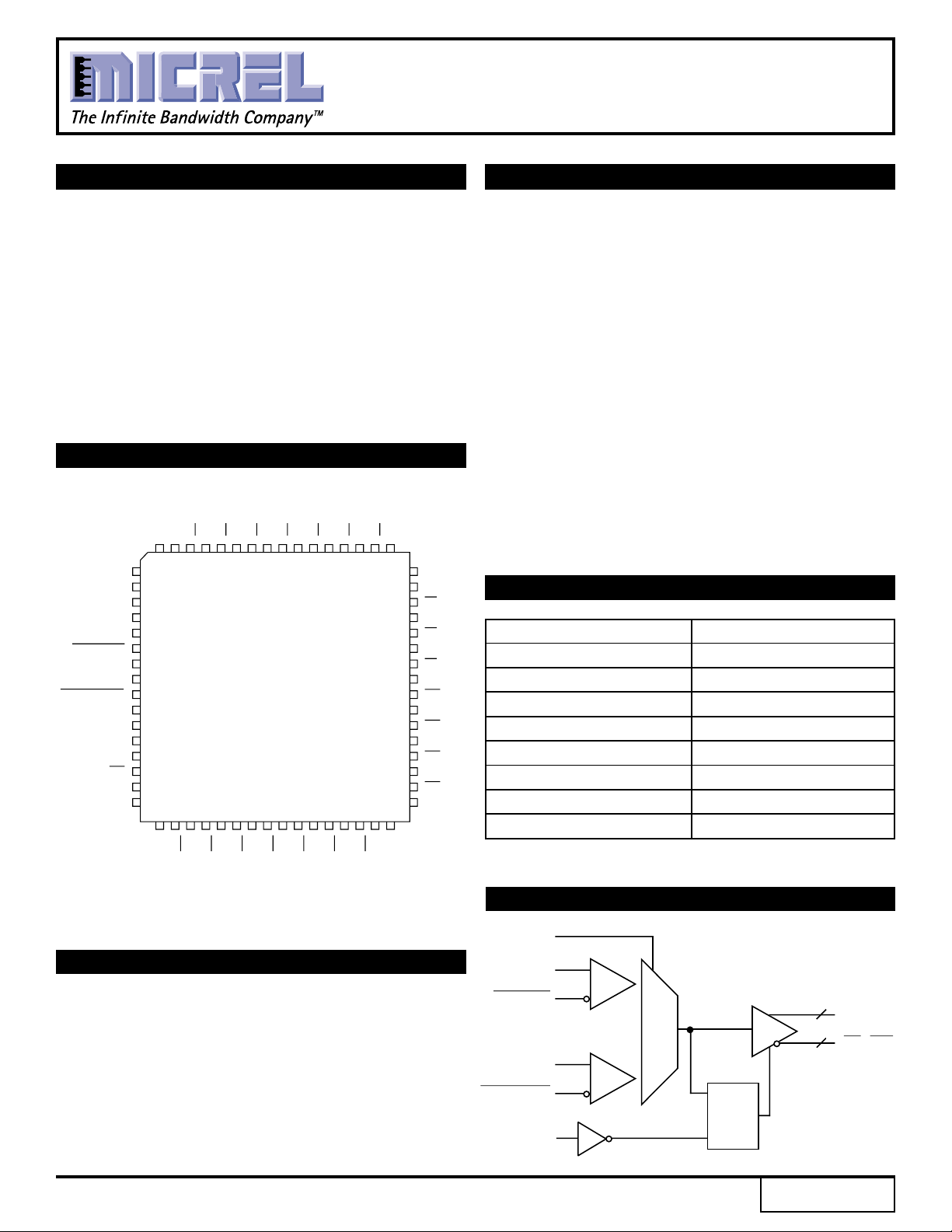
PIN CONFIGURATION
6
30 31 32
V
CCO
CCO
48
V
CCO
47
Q
7
46
Q
7
45
Q
8
44
Q
8
43
Q
9
42
Q
9
41
Q
10
40
Q
10
39
Q
11
38
Q
11
37
Q
12
36
Q
12
35
Q
13
34
Q
13
33
V
CCO
V
CCO
NC
NC
V
CCI
HSTL_CLK
HSTL_CLK
CLK_SEL
LVPECL_CLK
LVPECL_CLK
GND
OE
NC
NC
Q
Q
V
CCO
V
CCO
Q1Q1Q2Q
Q0Q
0
61 60 59 58 57 56 55 54 53 52 51 50 49
626364
1
2
3
4
5
6
7
8
9
10
11
12
13
14
21
15
21
16
17 18 19 20 21 22 23 24 25 26 27 28 29
Q19Q19Q18Q
Q20Q
V
CCO
20
Q3Q3Q4Q
2
64-PIN
HQFP
Q17Q17Q16Q
18
Q5Q5Q6Q
4
Q15Q15Q14Q14V
16
DESCRIPTION
The SY89824L is a High Performance Bus Clock Driver
with 22 differential HSTL (High Speed Transceiver Logic)
output pairs. The part is designed for use in low voltage
(3.3V/1.8V) applications which require a large number of
outputs to drive precisely aligned, ultra low skew signals to
their destination. The input is multiplexed from either HSTL
or LVPECL (Low Voltage Positive Emitter Coupled Logic)
by the CLK_SEL pin. The Output Enable (OE) is
synchronous so that the outputs will only be enabled/
disabled when they are already in the LOW state. This
avoids any chance of generating a runt clock pulse when
the device is enabled/disabled as can happen with an
asynchronous control.
The SY89824L features low pin-to-pin skew (50ps max.)
and low part-to-part skew (200ps max.)—performance
previously unachievable in a standard product having such
a high number of outputs. The SY89824L is available in a
single space saving package, enabling a lower overall cost
solution.
PIN NAMES
Pin Function
HSTL_CLK, /HSTL_CLK Differential HSTL Inputs
LVPECL_CLK, /LVPECL_CLK Differential LVPECL Inputs
CLK_SEL Input CLK Select (LVTTL)
OE Output Enable (LVTTL)
Q0-Q21, /Q0-/Q21 Differential HSTL Outputs
GND Ground
VCCI VCC Core
CCO VCC Output
V
APPLICATIONS
■ High-performance PCs
■ Workstations
■ Parallel processor-based systems
■ Other high-performance computing
■ Communications
LOGIC SYMBOL
CLK_SEL
HSTL_CLK
HSTL_CLK
LVPECL_CLK
LVPECL_CLK
OE
1
0
22
Q0 - Q21
22
Q0 - Q21
1
LEN
Q
D
Rev.: C Amendment: /1
Issue Date:
March 2000
Page 2
Micrel
ClockWorks™
SY89824L
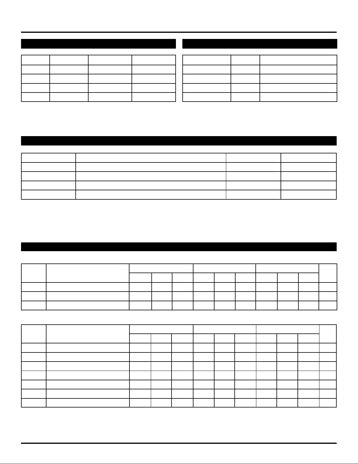
TRUTH TABLE
(1)
OE
0 0 LOW HIGH
0 1 LOW HIGH
1 0 HSTL_CLK /HSTL_CLK
1 1 LVPECL_CLK /LVPECL_CLK
NOTE:
1. The OE (output enable) signal is synchronized with the low level of the
HSTL_CLK and LVPECL_CLK signal.
ABSOLUTE MAXIMUM RATINGS
CLK_SEL Q0-Q21 /Q0-/Q21
(1)
SIGNAL GROUPS
Level Direction Signal
HSTL Input HSTL_CLK, /HSTL_CLK
HSTL Output Q0-Q21, /Q0-/Q21
LVPECL Input LVPECL_CLK, /LVPECL_CLK
LVCMOS/LVTTL Input CLK_SEL, OE
Symbol Rating Value Unit
VCCI/VCCO VCC Pin Potential to Ground Pin –0.5 to +4.0 V
VIN Input Voltage –0.5 to VCCI V
IOUT DC Output Current (Output HIGH) –50 mA
Tstore Storage Temperature –65 to +150 °C
NOTE:
1. Permanent device damage may occur if ABSOLUTE MAXIMUM RATINGS are exceeded. This is a stress rating only and functional operation is not
implied at conditions other than those detailed in the operational sections of this data book. Exposure to ABSOLUTE MAXIMUM RATING conditions
for extended periods may affect device reliability.
DC ELECTRICAL CHARACTERISTICS
Power Supply
TA = 0°CTA = +25°CTA = +70°C
Symbol Parameter Min. Typ. Max. Min. Typ. Max. Min. Typ. Max. Unit
VCCI VCC Core 3.0 3.3 3.6 3.0 3.3 3.6 3.0 3.3 3.6 V
VCCO VCC Output 1.6 1.8 2.0 1.6 1.8 2.0 1.6 1.8 2.0 V
CCI ICC Core — 115 140 — 115 140 — 115 140 mA
I
HSTL
TA = 0°CTA = +25°CTA = +70°C
Symbol Parameter Min. Typ. Max. Min. Typ. Max. Min. Typ. Max. Unit
(1)
(1)
1.0 — 1.2 1.0 — 1.2 1.0 — 1.2 V
0 — 0.4 0 — 0.4 0 — 0.4 V
VOH Output HIGH Voltage
VOL Output LOW Voltage
VIH Input HIGH Voltage VX +0.1 — 1.6 VX +0.1 — 1.6 VX +0.1 — 1.6 V
VIL Input LOW Voltage –0.3 — VX –0.1 –0.3 — VX –0.1 –0.3 — VX –0.1 V
VX Input Crossover Voltage 0.68 — 0.9 0.68 — 0.9 0.68 — 0.9 V
IIH Input HIGH Current +20 —–350 +20 —–350 +20 —–350 µA
IL Input LOW Current ——–500 ——–500 ——–500 µA
I
NOTE:
1. Outputs loaded with 50Ω to ground.
2
Page 3
Micrel
SY89824L
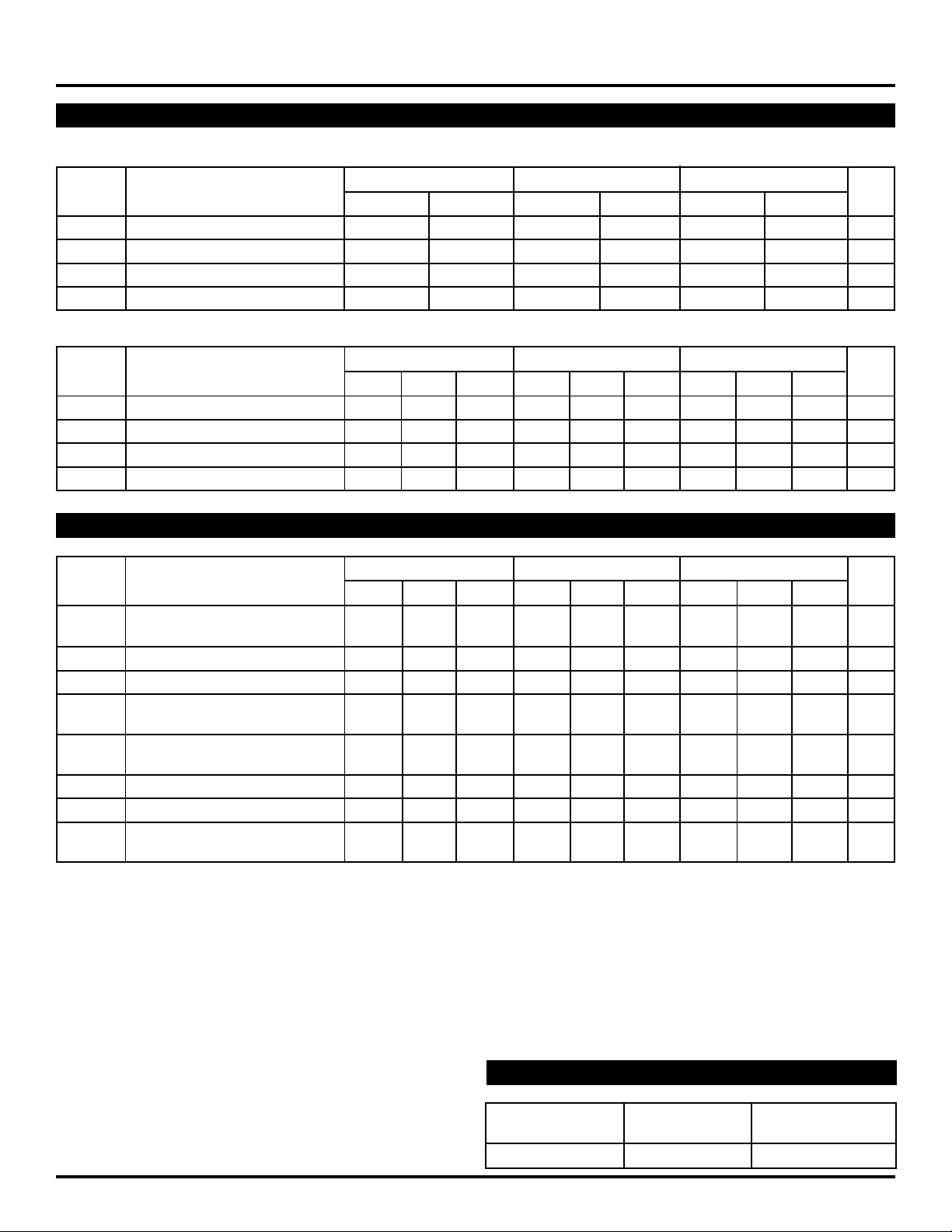
DC ELECTRICAL CHARACTERISTICS
LVPECL
TA = 0°CTA = +25°CTA = +70°C
Symbol Parameter Min. Max. Min. Max. Min. Max. Unit
VIH Input HIGH Voltage VCCI – 1.165 VCCI – 0.880 VCCI – 1.165 VCCI – 0.880 VCCI – 1.165 VCCI – 0.880 V
VIL Input LOW Voltage VCCI – 1.810 VCCI – 1.475 VCCI – 1.810 VCCI – 1.475 VCCI – 1.810 VCCI – 1.475 V
IIH Input HIGH Current — +150 — +150 — +150 µA
I
IL Input LOW Current 0.5 — 0.5 — 0.5 — µA
LVCMOS/LVTTL
TA = 0°CTA = +25°CTA = +70°C
Symbol Parameter Min. Typ. Max. Min. Typ. Max. Min. Typ. Max. Unit
VIH Input HIGH Voltage 2.0 ——2.0 ——2.0 ——V
VIL Input LOW Voltage ——0.8 ——0.8 ——0.8 V
IIH Input HIGH Current +20 —–250 +20 —–250 +20 —–250 µA
I
IL Input LOW Current ——–600 ——–600 ——–600 µA
ClockWorks™
AC ELECTRICAL CHARACTERISTICS
(1)
TA = 0°CTA = +25°CTA = +70°C
Symbol Parameter Min. Typ. Max. Min. Typ. Max. Min. Typ. Max. Unit
t
PHL Propagation Delay
(2)
— 1.0 ——1.0 ——1.0 — ns
tPLH
(4)
(3)
(5)
——50 ——50 ——50 ps
——200 ——200 ——200 ps
600 ——600 ——600 ——mV
tskew Within-Device Skew
tskpp Part-to-Part Skew
VPP Minimum Input Swing
LVPECL_CLK
V
CMR Common Mode Range
(6)
–1.5 —–0.4 –1.5 —–0.4 –1.5 —–0.4 V
LVPECL_CLK
tS OE Set-Up Time
(7)
1.0 ——1.0 ——1.0 ——ns
tH OE Hold Time 0.5 ——0.5 ——0.5 ——ns
t
r Output Rise/Fall Time 300 — 800 300 — 800 300 — 800 ps
tf (20% – 80%)
NOTES:
1. Outputs loaded with 50Ω to ground. Airflow ≥ 300 LFPM.
2. Differential propagation delay is defined as the delay from the crossing point of the differential input signals to the crossing point of the differential
output signals.
3. The within-device skew is defined as the worst case difference between any two similar delay paths within a single device operating at the same
voltage and temperature.
4. The part-to-part skew is defined as the absolute worst case difference between any two delay paths on any two devices operating at the same
voltage and temperature.
5. The VPP (min.) is defined as the minimum input differential voltage which will cause no increase in the propagation delay.
6. VCMR is defined as the range within which the VIH level may vary, with the device still meeting the propagation delay specification. The numbers in
the table are referenced to VCCI. The VIL level must be such that the
peak-to-peak voltage is less than 1.0V and greater than or equal to
VPP (min.). The lower end of the CMR range varies 1:1 with VCCI. The
VCMR (min) will be fixed at 3.3V – |VCMR (min)|.
7. OE set-up time is defined with respect to the rising edge of the clock.
OE HIGH to LOW transition ensures outputs remain disabled during
the next clock cycle. OE LOW to HIGH transition enables normal
operation of the next input clock.
PRODUCT ORDERING CODE
Ordering Package Operating
Code Type Range
SY89824LHC H64-1 Commercial
3
Page 4
Micrel
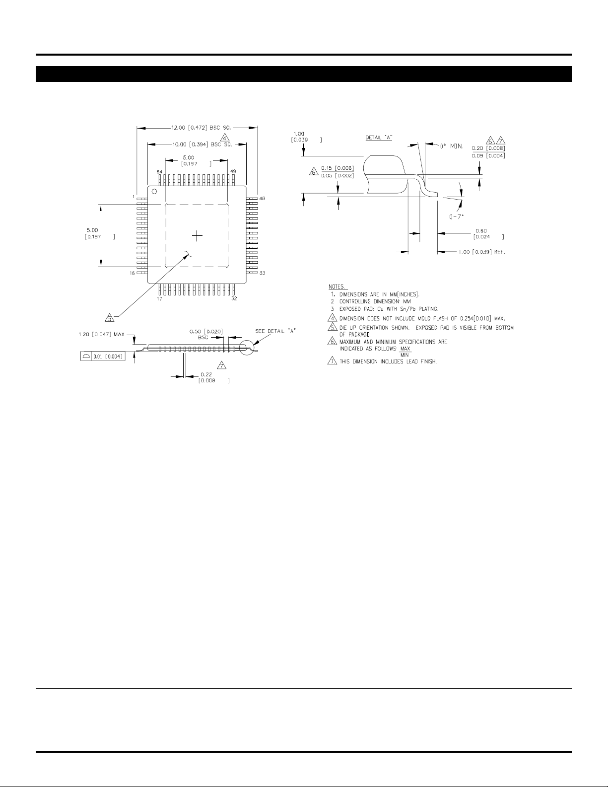
64 LEAD EPAD-TQFP (DIE UP) (H64-1)
+0.05
–0.05
+0.012
–0.012
+0.05
–0.05
+0.002
–0.002
ClockWorks™
SY89824L
+0.03
–0.03
+0.012
–0.012
+0.05
–0.05
+0.002
–0.002
+0.15
–0.15
+0.006
–0.006
Rev. 02
MICREL-SYNERGY 3250 SCOTT BOULEVARD SANTA CLARA CA 95054 USA
TEL + 1 (408) 980-9191 FAX + 1 (408) 914-7878 WEB http://www.micrel.com
This information is believed to be accurate and reliable, however no responsibility is assumed by Micrel for its use nor for any infringement of patents or
other rights of third parties resulting from its use. No license is granted by implication or otherwise under any patent or patent right of Micrel Inc.
© 2000 Micrel Incorporated
4
 Loading...