

Page 1
LASER DIODE
CONTROLLER
WITH APC
SY88905
FEATURES
■ DC bias current adjustable to 25mA
■ Buffered Loss-of-Signal output when used with
SY88903
■ Monitor Diode power control circuit
■ Designed for use with SY88902 and SY88903
■ Single power supply
■ Available in 10-pin (3mm) MSOP
PIN CONFIGURATION
1LOS
LOS
OUT
GND
I
BIAS
V
CC
IN
2
MSOP
3
K10-1
4
5
10 V
9
8
7
6
REF
I
BIAS SET
I
BIAS FB
I
PIN SET
MD
DESCRIPTION
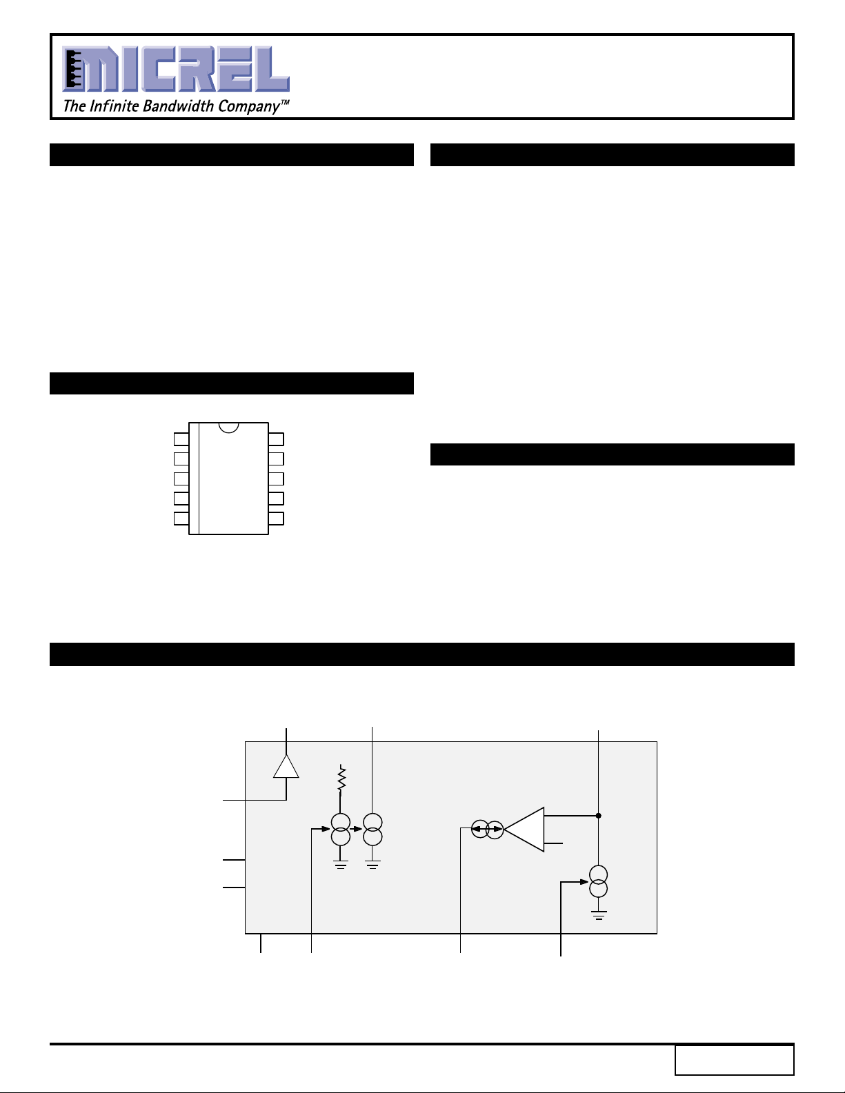
The SY88905 is an integrated Laser Diode controller for
the SY88902 Laser Driver and SY88903 Laser Receiver
that provides power control functions for a complete module
solution. The SY88905 is designed to provide the laser
diode with an independent DC threshold current (IBIAS)
source to assure optimum laser diode performance. The
SY88905 also provides buffered Loss-of-Signal (LOS) output
in PECL level. The device is designed for fast and accurate
calibration of the laser diode.
Once the optimal operating point is determined and set
for a specific laser diode, the threshold current (IBIAS) is
designed to automatically compensate for laser diode aging
and module temperature.
APPLICATIONS
■ Controller for High Speed Optical Data Transmission
■ 1.25Gbps Gigabit Ethernet
■ 531 Mbps and 1062Mbps Fibre Channel
■ 622Mbps SONET
■ Gigabit Interface Converter
BLOCK DIAGRAM
LOSIN
GND
VCC
LOSOUT
VREF
VREF2
IBIAS SET
IBIAS
40X
1
IBIAS FB
MD
-
+
VREF 2
IPIN SET
Rev.: B Amendment: /1
Issue Date: July 2000
Page 2
Micrel
PIN DEFINITIONS
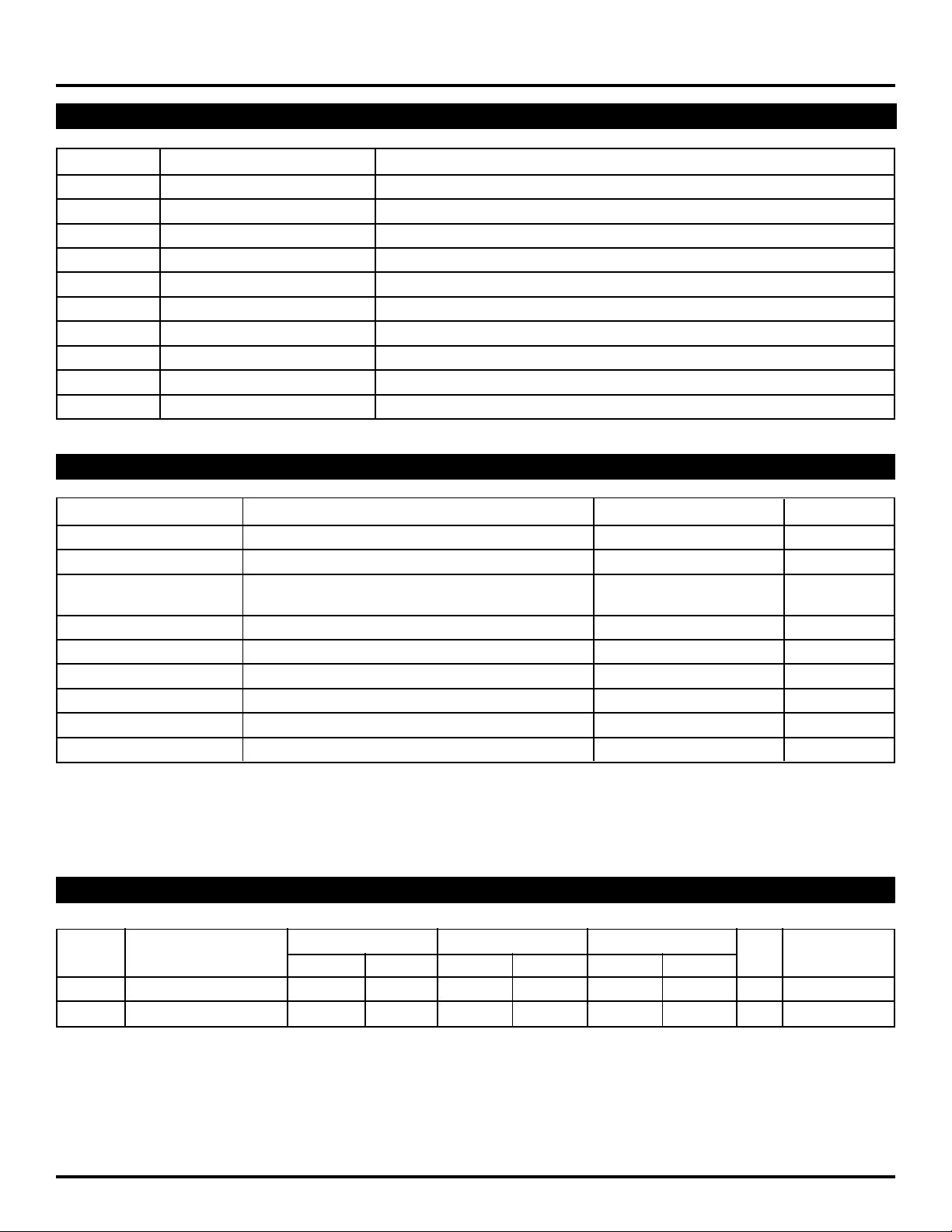
Pin Type Description
VCC Power Positive Power supply
GND Power Ground
LOSIN TTL Input Loss-of-Signal Input from SY88903
VREF Analog Output Reference Voltage
IPIN SET Analog Input Adjustable, Resistor to VREF sets Monitor Diode Photo Current Reference
LOSOUT PECL Output Loss-of-Signal PECL output
IBIASFB Analog Output Monitor Diode Feedback
IBIASSET Analog Input Adjustable, Resistor to VREF sets the DC bias current for the Laser Diode
MD Analog Input Monitor Diode Connection
BIAS Analog Input DC bias current for the Laser Diode
I
SY88905
ABSOLUTE MAXIMUM RATINGS
LOGIC DIAGRAM
(1)
Symbol Rating Value Unit
VCC Power Supply Voltage 0 to +7.0 V
LOSIN Input Voltage 0 to VCC V
OUT, IPIN SET Others; I/O Voltage –0.3, VCC +0.3 V
LOS
IBIASFB, IBIAS SET
TA Operating Temperature Range 0 to +85 ˚C
Tstore Storage Temperature Range –55 to +125 ˚C
IPIN SET, IBIAS SET, IMD Max. Sink Current 1 mA
IBIASFB Max. Source Current 1 mA
IBIAS Max. Sink Current 30 mA
VREF Max. Source Current 2 mA
I
NOTE:
1. Permanent device damage may occur if ABSOLUTE MAXIMUM RATINGS are exceeded. This is a stress rating only and functional operation is not implied
at conditions other than those detailed in the operational sections of this data sheet. Exposure to ABSOLUTE MAXIMUM RATlNG conditions for extended
periods may affect device reliability.
100H ECL DC ELECTRICAL
(1)
VCC = +5V ±10%
T
A = 0°CTA = +25°CTA = +85°C
Symbol Parameter Min. Max. Min. Max. Min. Max. Unit Condition
VOH Output HIGH Voltage
OL Output LOW Voltage
V
NOTE:
1. 100H circuits are designed to meet the DC specifications shown in the table where transverse airflow greater than 500lfpm is maintained.
VCC– 1025 VCC– 880 VCC– 1025 VCC– 880 VCC– 1025 VCC– 880
VCC –1810 VCC –1620 VCC –1810 VCC –1620 VCC –1810 VCC–1620
mV 50Ω to VCC–2V
mV 50Ω to VCC–2V
2
Page 3
Micrel
SY88905
DC ELECTRICAL CHARACTERISTICS
VCC = +5V ±10%
TA = 0°CTA = +25°CTA = +85°C
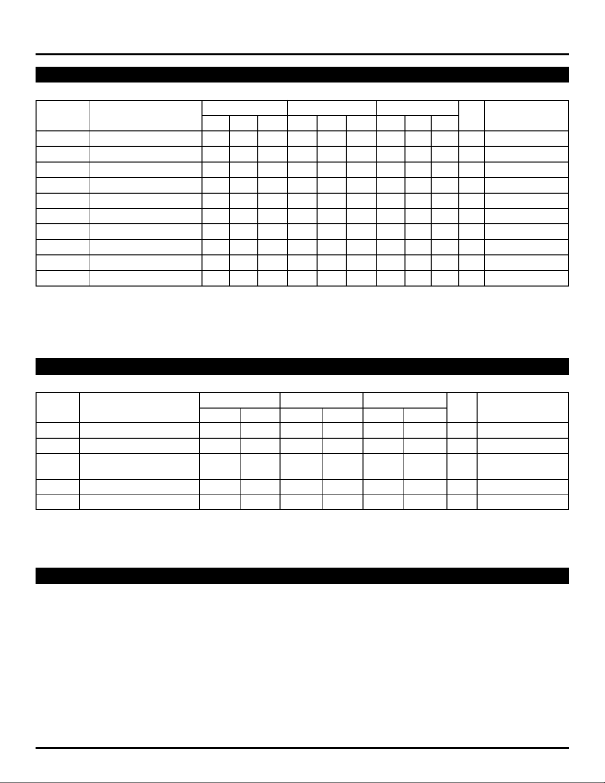
Symbol Parameter Min. Typ. Max. Min. Typ. Max. Min. Typ. Max. Unit Conditions
ICC Power Supply Current — — 40 — 28 40 — — 40 mA No output load
IBIAS SET IBIAS SET Input Current — — 0.9 — — 0.9 — — 0.9 mA
IBIAS IBIAS Output Current 0.5 — 25 0.5 — 25 0.5 — 25 mA
ABIAS IBIAS Current Gain 28 — 44 28 37 44 28 — 44 =IBIAS / IBIAS SET
VREF Reference Voltage 2.30 — 3.30 2.30 2.75 3.30 2.30 — 3.30 V IREF = -100µA
∆VPIN SET VPIN SET Voltage Tracking 0.95 — 1.35 0.95 1.13 1.35 0.95 — 1.35 V =VREF – VPIN SET
∆VBIAS SET VBIAS Voltage Tracking 0.8 — 1.20 0.8 1.0 1.20 0.8 — 1.20 V =VREF – VBIAS SET
VCOMP BIAS Compliance Voltage 0.1 — 1.0 0.1 0.4 1.0 0.1 — 1.0 V IBIAS = 15mA
(2)
(1)
350 — — 350 500 — 350 — — µA
4 — 14 4 — 14 4 — 14
IBIAS FB Feedback Current
BIAS FB Feedback Gain
A
NOTE:
1. |IMD – IPIN SET| = 100µA
2. |IBIAS FB| / |IMD – IPIN SET|
TTL DC ELECTRICAL CHARACTERISTICS
VCC = +5V ±10%
TA = 0°CTA = +25°CTA = +85°C
Symbol Parameter Min. Max. Min. Max. Min. Max. Unit Condition
VIH Input HIGH Voltage 2.0 — 2.0 — 2.0 — V —
VIL Input LOW Voltage — 0.8 — 0.8 — 0.8 V —
IH Input HIGH Current — 20 — 20 — 20 µAVIN = 2.7V
I
— 100 — 100 — 100 VIN = VCC
IIL Input LOW Current — –0.3 — –0.3 — –0.3 mA VIN = 0.5V
V
IK Input Clamp Voltage — –1.2 — –1.2 — –1.2 V IIN = –12mA
NOTE:
1. Individual product specifications over-ride general specifications.
DETAILED DESCRIPTION
The SY88905 is an integrated control circuit for laser
diode modules intended for high-frequency fiber-optic
applications. The device is designed to operate with the
SY88902 laser diode driver providing Automatic Power
Control (APC) which provides bias current control and
monitor diode interface. The device also interfaces with the
SY88903 high-speed limiting amplifier providing chatter-free
Loss of Signal function.
Laser Diode Supply Current
The SY88905 provides the adjustable drive current for
the laser diode, DC bias.
Monitor Diode
The MD pin on the SY88905 provides low frequency
light intensity, laser power out feedback from the monitor
diode in the laser diode package. This feedback is used to
adjust the IBIAS level through the Automatic Power Control
circuit to maintain a near constant power output from the
laser diode.
3
Page 4
Micrel
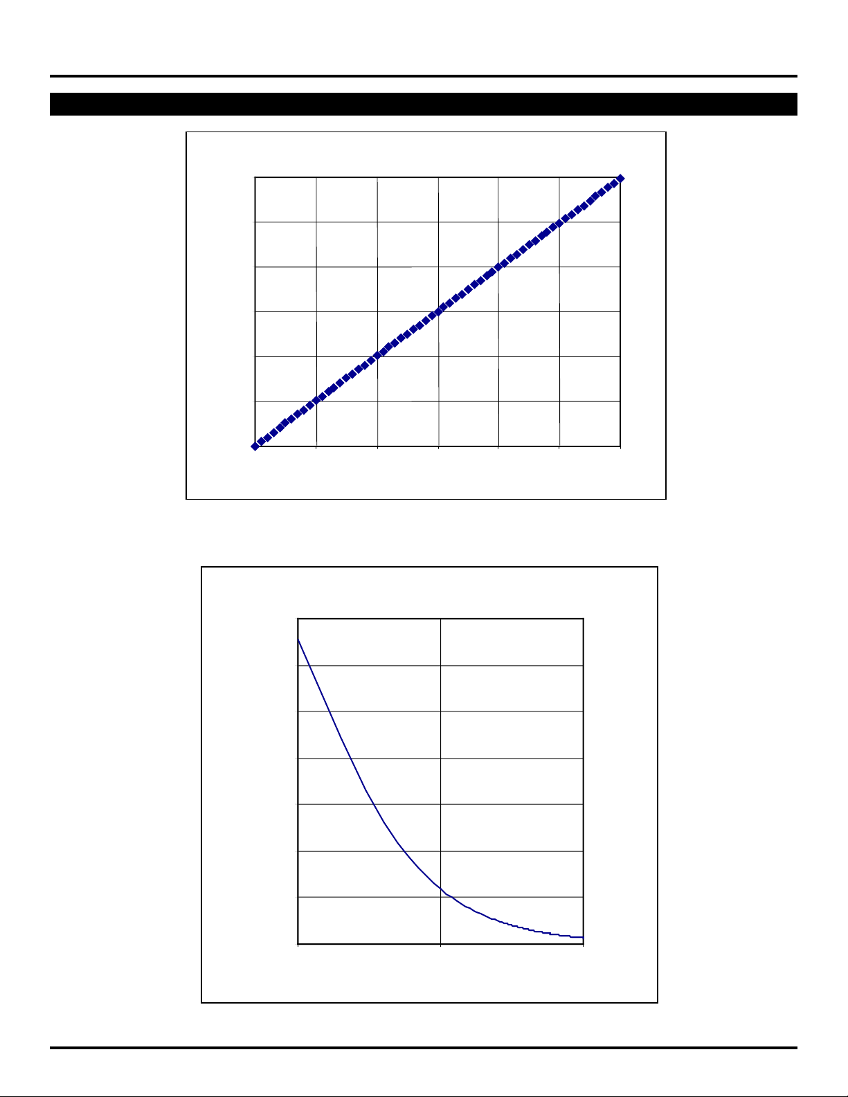
SIMULATION GRAPHS
3.5E-02
3.0E-02
2.5E-02
2.0E-02
(A)
BIAS
I
1.5E-02
1.0E-02
5.0E-03
SY88905
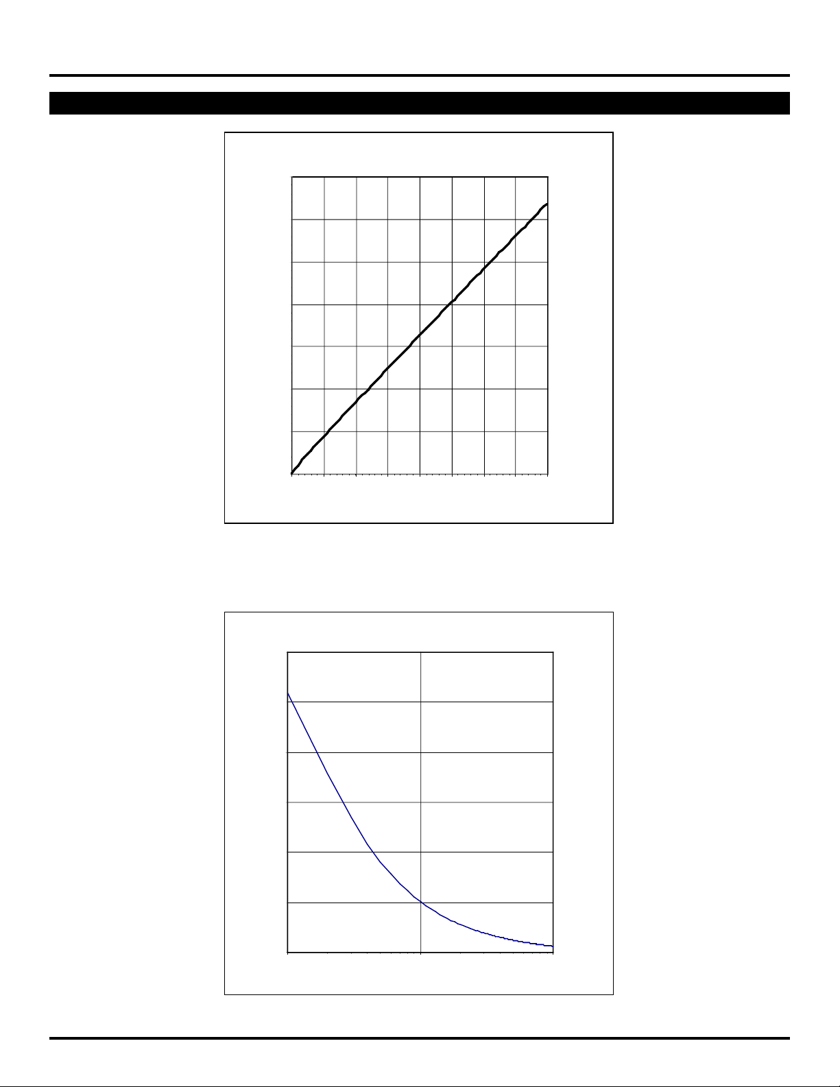
IBIAS vs IBIAS SET
0.0E+00
0.E+00 1.E-04 2.E-04 3.E-04 4.E-04 5.E-04 6.E-04 7.E-04 8.E-04
IBIAS SET (A)
Figure 1. IBIAS v. IBIAS SET
I
BIAS
vs R
BIAS SET
3.00E-02
2.50E-02
2.00E-02
(A)
1.50E-02
BIAS
I
1.00E-02
5.00E-03
0.00E+00
1.00E+03 1.00E+04 1.00E+05
BIAS SET
(Ohm)
R
Figure 2. IBIAS v. RBIAS SET
4
Page 5
Micrel
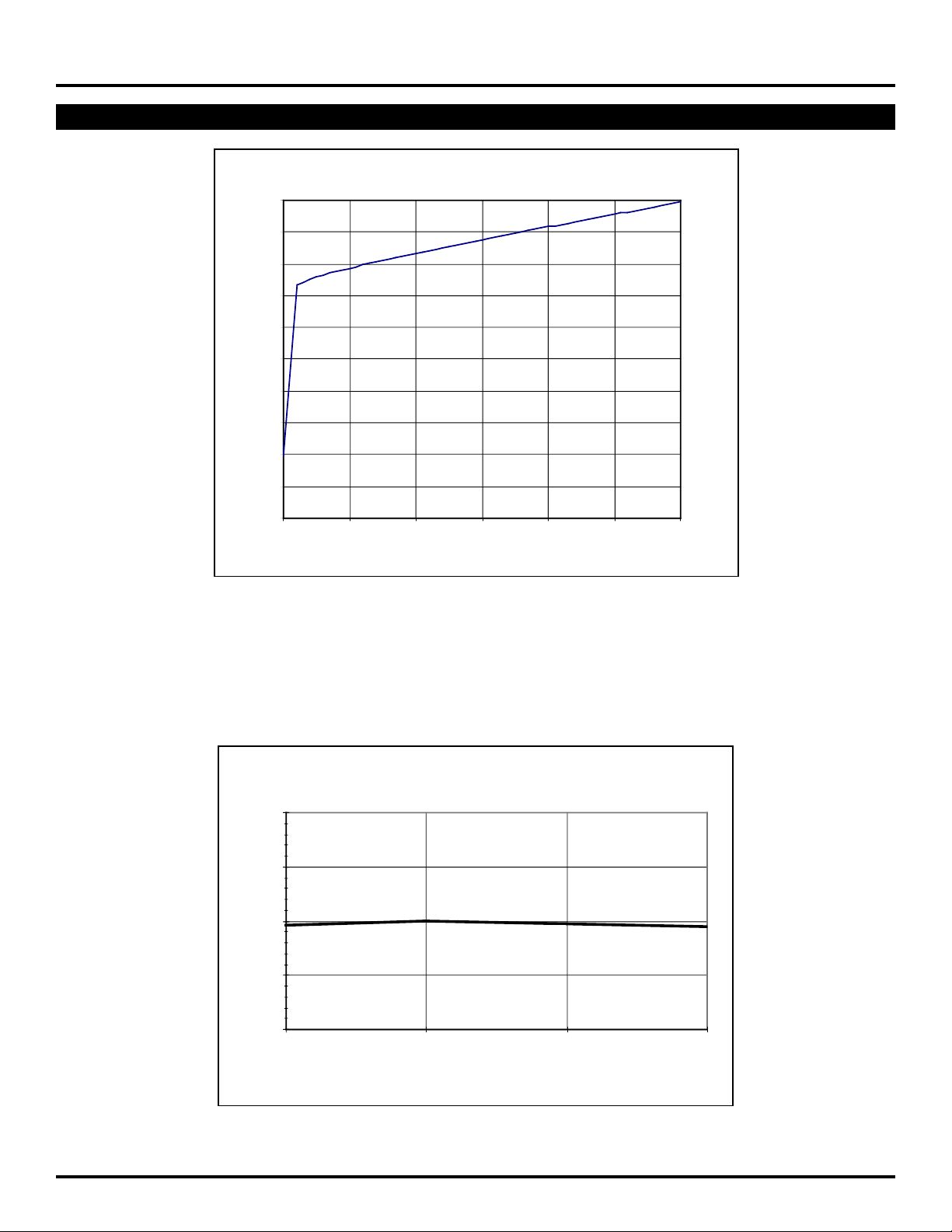
SIMULATION GRAPHS
IPIN vs IPINSET
6.E-04
5.E-04
4.E-04
3.E-04
PIN (A)
I
2.E-04
1.E-04
0.E+00
0.E+00 1.E-04 2.E-04 3.E-04 4.E-04 5.E-04 6.E-04
IPIN SET (A)
SY88905
7.00E-04
6.00E-04
5.00E-04
4.00E-04
(A)
PIN SET
3.00E-04
I
2.00E-04
1.00E-04
Figure 3. IPIN v. IPIN SET
I
PIN SET
vs R
IPIN SET
0.00E+00
1.00E+03 1.00E+04 1.00E+05
R
IPIN SET
(A)
Figure 4. IPIN SET v. RPIN SET
5
Page 6
Micrel
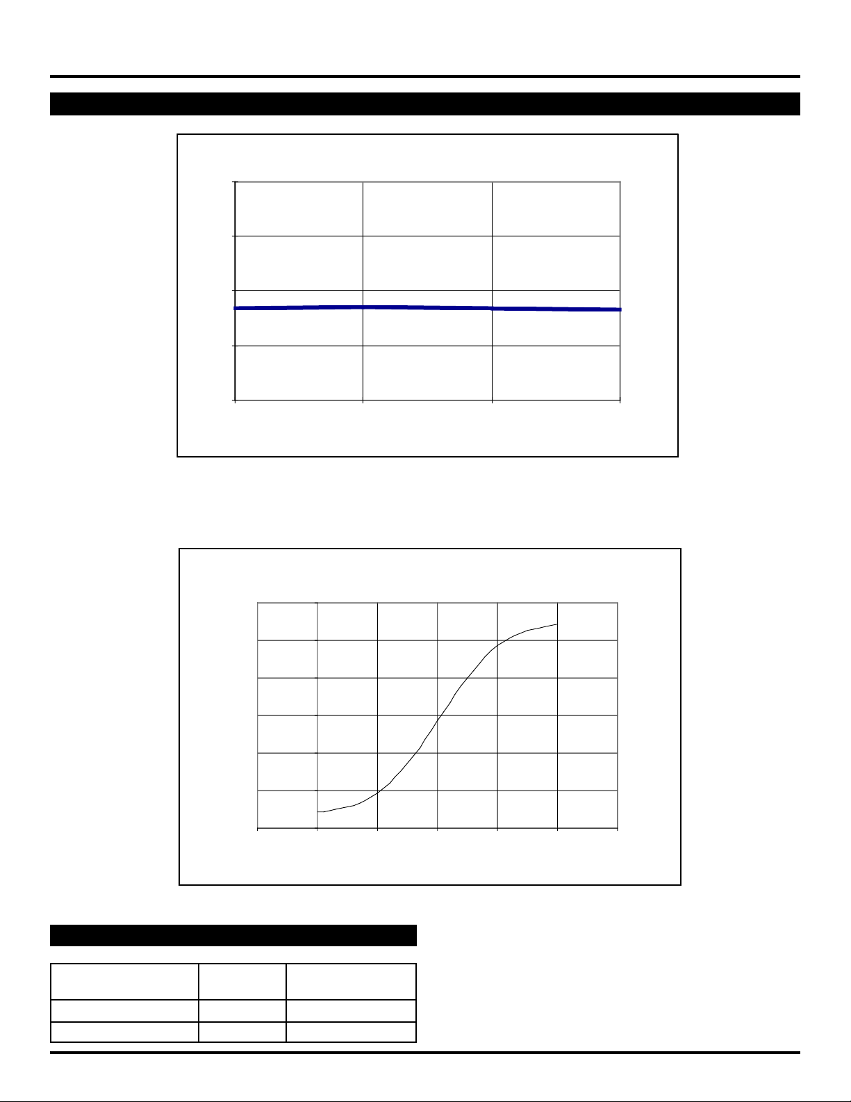
SIMULATION GRAPHS
V
IPIN SET
vs I
PIN SET
2
1.8
1.6
1.4
1.2
(V)
1
IPIN SET
V
0.8
0.6
0.4
0.2
0
0.00E+00 1.00E-04 2.00E-04 3.00E-04 4.00E-04 5.00E-04 6.00E-04
PIN SET
(A)
I
SY88905
Figure 5. V IPIN SET v. IPIN SET
Typical Vbiasset Voltage Tracking
1.1
1.05
1
Vref - Vbiasset (V)
0.95
0.9
04080120
Junction Temperature (deg C)
Figure 6. Typical VBIAS SET Voltage Tracking
6
Page 7
Micrel
SIMULATION GRAPHS
SY88905
Typical V
1.25
1.20
PIN SET
Voltage Tracking
(V)
1.15
BIAS SET
- V
REF
1.10
V
1.05
0C 40C 80C 120C
Junction Temperature (deg C)
Figure 7. Typical VPIN SET Voltage Tracking
0.0006
0.0004
0.0002
(A)
0
BIAS FB
I
-0.0002
-0.0004
-0.0006
-1.50E-04 -1.00E-04 -5.00E-05 0.00E+00 5.00E-05 1.00E-04 1.50E-04
PRODUCT ORDERING CODE
Ordering Package Operating
Code Type Range
SY88905KC K10-1 Commercial
SY88905KCTR K10-1 Commercial
IBIAS FB vs IMD - IPIN SET (IPIN SET =100 uA)
IMD - I
PIN SET
(A)
Figure 8. IBIAS FB VS. IMD - IPIN SET
7
Page 8
Micrel
OUT
V
CC
V
EE
SY88905
D
IN
D
IN
LOS
OUT
Gigabit EthernetTerminal
V
CC
OUT
I
BIAS
EN
LOSEN
MD
D
OUT
D
OUT
D
IN
D
IN
V
CC
V
EE
SY88902
SY88903
V
CC
V
CC
V
BIAS SET
I
BIAS SET
Laser
Module
PECL
R
EXT
R
SER
–RX_DAT
+RX_DAT
–TX_DATA
+TX_DAT
V
REF
R
SET
V
LVL
V
REF
LOS
IN
V
REF
I
BIAS FB
I
PIN SET
V
REF
RX_LOS
V
BB
V
CC
I
BIAS SET
V
PIN SET
GND
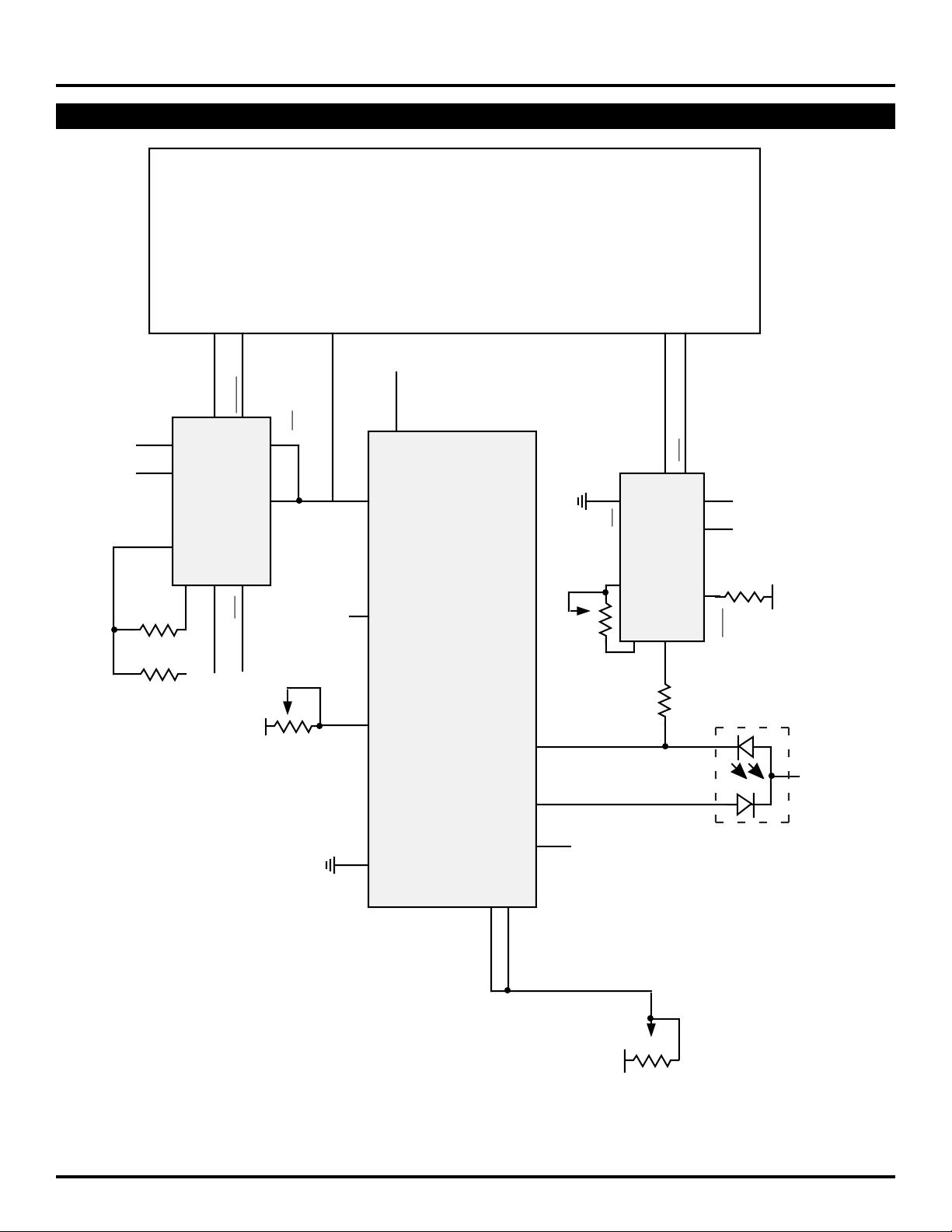
APPLICATION EXAMPLE FOR 3-CHIP SET SOLUTION
SY88905
8
Page 9
Micrel
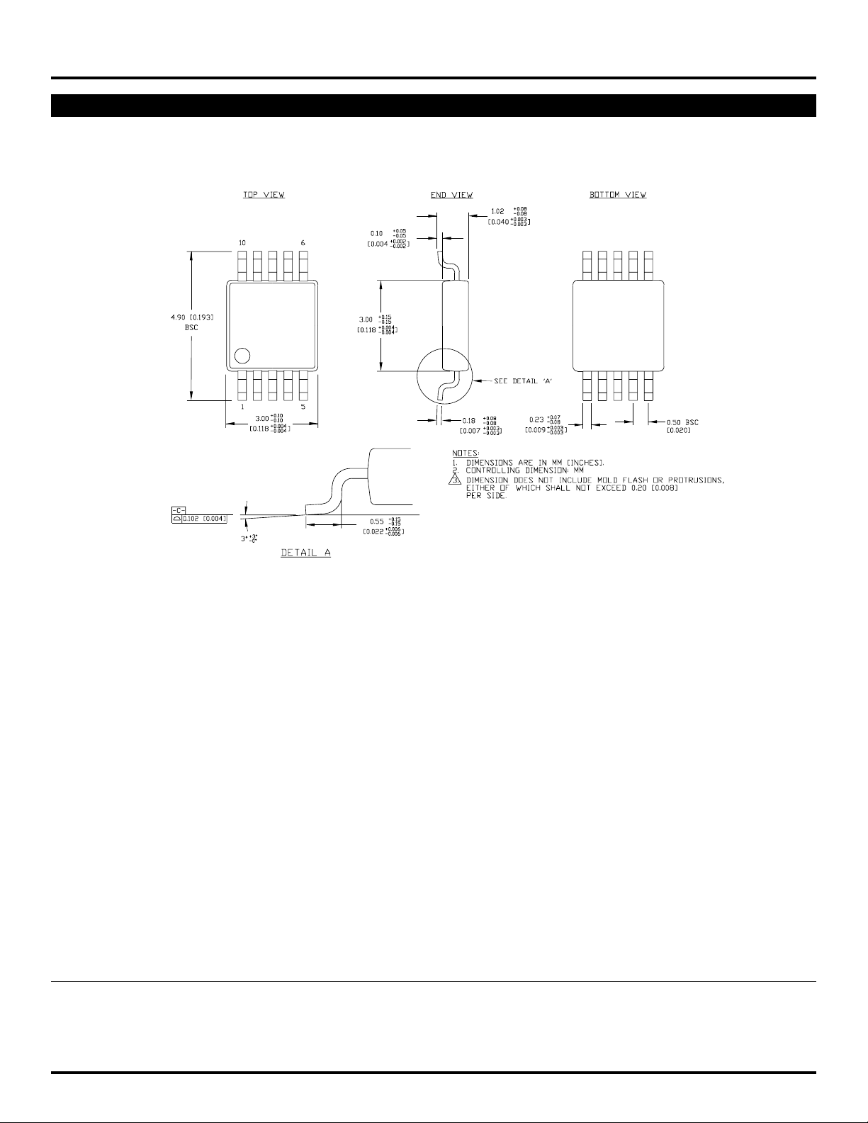
10 LEAD MSOP (K10-1)
SY88905
Rev. 00
MICREL-SYNERGY 3250 SCOTT BOULEVARD SANTA CLARA CA 95054 USA
TEL + 1 (408) 980-9191 FAX + 1 (408) 914-7878 WEB http://www.micrel.com
This information is believed to be accurate and reliable, however no responsibility is assumed by Micrel for its use nor for any infringement of patents or
other rights of third parties resulting from its use. No license is granted by implication or otherwise under any patent or patent right of Micrel Inc.
© 2000 Micrel Incorporated
9
 Loading...