

Page 1
5V/3.3V
FREQUENCY SYNTHESIZER
(60MHz to 1GHz)
FEATURES DESCRIPTION
ClockWorks™
SY89424V
■ 3.3V and 5V power supply options
■ Up to 1GHz clock frequencies
■ Internal quartz reference oscillator driven by quartz
crystal or PECL source
■ Low jitter PLL design
■ On-chip 20 ohm driver
■ Differential outputs with 600mV (min) swing
■ Optional pull-down resistors for AC-coupled outputs
■ Low power consumption
■ External loop filter optimizes performance/cost
■ Available in 16-pin SOIC package
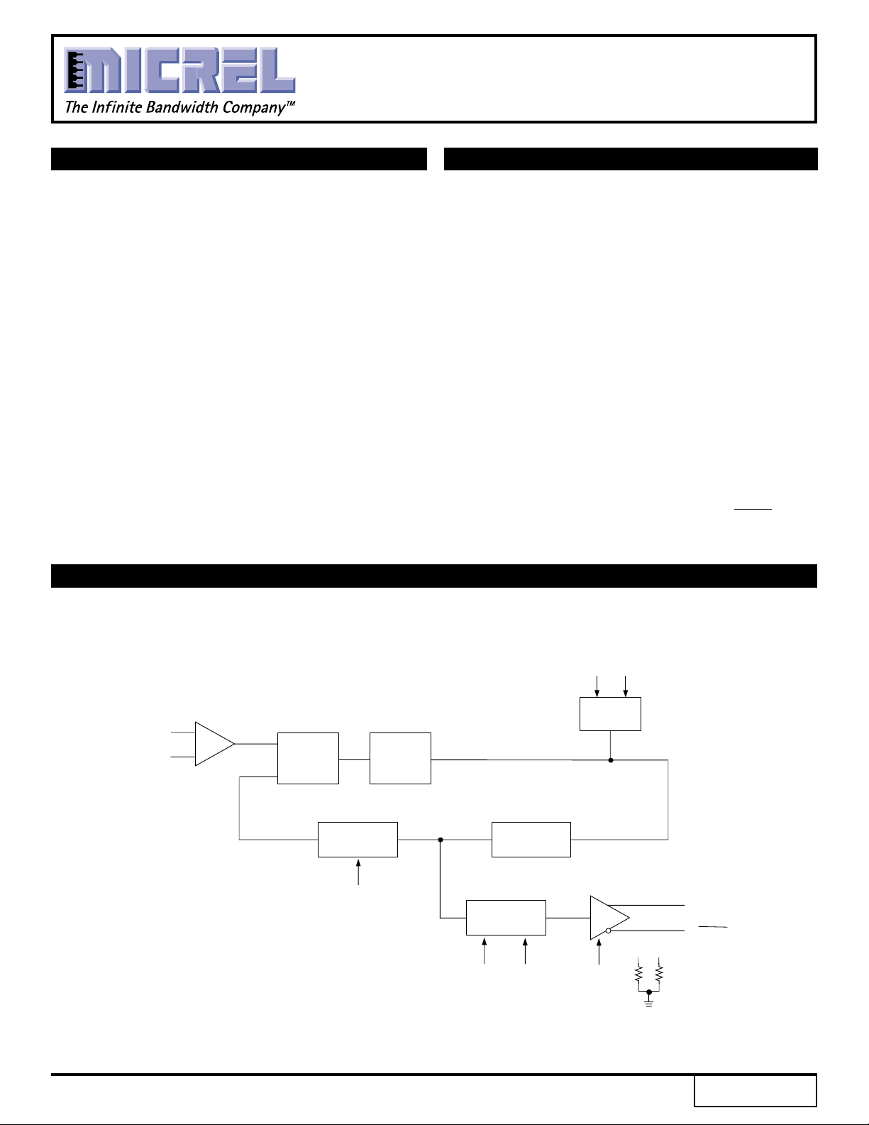
BLOCK DIAGRAM
The SY89424V is a low-power Phase Locked Loop
(PLL) based frequency synthesizer. The device is capable
of generating up to 1GHz clock frequencies with a low-cost
10–25MHz external series-resonant quartz crystal. One
can also use PECL differential clock signals to drive this
device instead of the quartz crystal. Operation of this chip
is controlled by three select pins (S1, S2 and S3). S1
selects the divide ratio of 24 or 50 for the PLL. S2 and S3
select the output frequency. There are two pull-down
resistor pins (PDR1 and PDR2). Each pin has an on-chip
resistor that will control the output driver currents. When
PDR1 and PDR2 pins are open, both outputs are normal
open emitter PECL drivers. When PDR1 and PDR2 pins
are shorted to the outputs, on-chip pull down currents of
25mA (40mA at 5V VCC) are provided. Both output drivers
are capable of driving 20 ohm clock lines. An output enable
(OE) pin is available and it can be HIGH or left open for
normal operation. When OE is LOW, a built-in Disable
Timing Synchronizer will force the FOUT output to LOW at
the completion of the HIGH clock cycle. The FOUT output
remains HIGH during that time.
XTAL1
XTAL2
OSC
PHASE
COMP
÷ 24, ÷ 50 VCO
CHARGE
PUMP
S1A
÷ 1, 2, 3, 4
S2A
S3A
F1A
LOOP
FILTER
OE
F2A
FOUT
FOUT
PDR1 PDR2
Rev.: G Amendment: /0
1
Issue Date: May, 1998
Page 2
Micrel
ClockWorks™
SY89424V
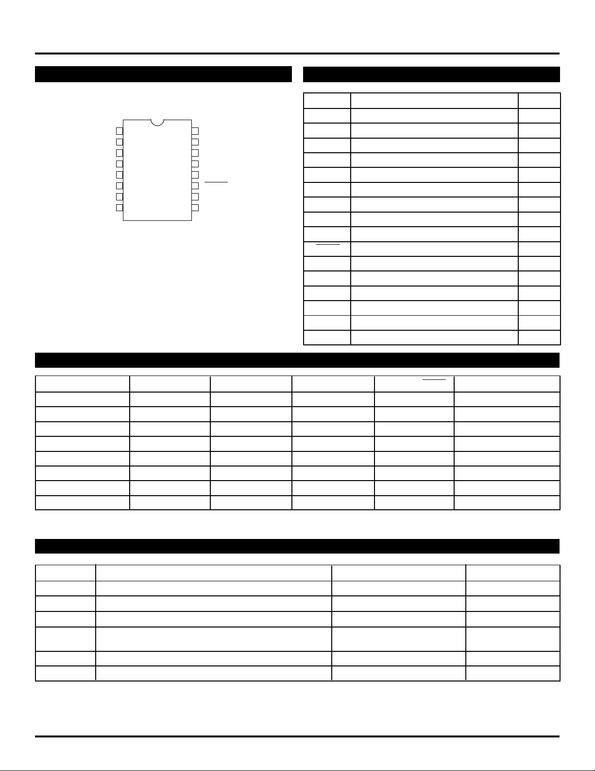
PIN CONFIGURATION
V
CCQ
XTAL
V
XTAL
V
116
2
2
EE
3
1
413
Top View
S1
CC
S3
S2
Gullwing
512
6
7
89
15
14
11
10
F1
F2
OE
PDR
FOUT
FOUT
PDR
V
CCO
PIN NAMES
Pin Function I/O
XTAL1 Crystal Input 1 (PECL) I/O
XTAL2 Crystal Input 2 (PECL) I/O
F1 Filter Pin 1 —
1
2
F2 Filter Pin 2 (Reference) —
VCCQ Positive Power Supply (Charge Pump) —
S1 Select Input 1 (TTL) I
S2 Select Input 2 (TTL) I
S3 Select Input 3 (TTL) I
FOUT Output (PECL) O
FOUT Complement Output (PECL) O
VCC Positive Power Supply (Logic) —
VCCO Positive Power Supply (PECL Outputs) —
OE Output Enable (TTL) I
VEE Negative Power Suppy (0.0V) —
PDR1 Pulldown Resistor (100Ω) —
2 Pulldown Resistor (100Ω) —
PDR
FREQUENCY SELECTION TABLE
Input S1 S2 S3 FOUT, FOUT Frequency Range MHz
(1)
FOSC
NOTE:
1. FOSC = 10MHz to 25MHz.
ABSOLUTE MAXIMUM RATING
Symbol Parameter Value Unit
VCC Power Supply Voltage –0.5 to +7.0 V
VI TTL Input Voltage
II TTL Input Current
I
OUT ECL Output Current –Continuous 50 mA
Tstore Storage Temperature –65 to +150 °C
T
A Operating Temperature 0 to +75 °C
NOTES:
1. Permanent device damage may occur if ABSOLUTE MAXIMUM RATINGS are exceeded. This is a stress rating only and functional operation is not
implied at conditions other than those detailed in the operational sections of this data sheet. Exposure to ABSOLUTE MAXIMUM RATING conditions
for extended periods may affect device reliability.
2. Either voltage limit or current limit is sufficient to protect input.
0 0 0 24X FOSC 240 – 480
0 0 1 12X FOSC 120 – 240
0 1 0 8X FOSC 80 – 160
0 1 1 6X FOSC 60 – 120
1 0 0 50X FOSC 500 – 1000
1 0 1 25X FOSC 250 – 500
1 1 0 16.67X FOSC 167 – 333
1 1 1 12.5X F
(1)
(2)
(2)
–0.5 to 6.0 V
–30 to +5.0 mA
OSC 125 – 250
–Surge 100
2
Page 3
ClockWorks™
Micrel
SY89424V
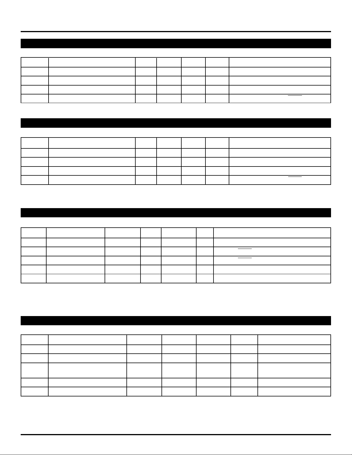
5V DC ELECTRICAL CHARACTERISTICS
VCC = VCCQ = VCCO = 4.75V to 5.25V
Symbol Parameter Min. Typ. Max. Unit Condition
VCC Power Supply Voltage 4.75 — 5.25 V VCC = VCCQ = VCCO
ICC Power Supply Current (VCC) ——80 mA
ICCQ Power Supply Current (VCCQ) ——10 mA
CCO Power Supply Current (VCCO) ——20 mA PECL outputs FOUT & FOUT are open
I
3.3V DC ELECTRICAL CHARACTERISTICS
VCC = VCCQ = VCCO = 3.0V to 5.25V
Symbol Parameter Min. Typ. Max. Unit Condition
VCC Power Supply Voltage 3.0 — 3.8 V VCC = VCCQ = VCCO
ICC Power Supply Current (VCC) ——68 mA
ICCQ Power Supply Current (VCCQ) —— 9mA
CCO Power Supply Current (VCCO) ——18 mA PECL outputs FOUT & FOUT are open
I
PECL DC ELECTRICAL CHARACTERISTICS
VCC = VCCQ = VCCO = 3.0V to 5.25V
Symbol Parameter Min. Typ. Max. Unit Condition
VO Output Voltage Swing 0.55 0.85 1.15 V Peak-to-Peak
VOH Output HIGH Voltage VCC – 1.075 — VCC – 0.800 V FOUT & FOUT loaded with 50Ω to VCC – 2.0V
VOL Output LOW Voltage VCC – 1.860 — VCC – 1.570 V FOUT & FOUT loaded with 50Ω to VCC – 2.0V
VIH Input HIGH Voltage
IL Input LOW Voltage
V
NOTE:
1. Forcing voltage at XTAL1 and XTAL2
(1)
VCC – 1.165 — VCC – 0.880 V
(1)
VCC – 1.810 — VCC – 1.475 V
TTL DC ELECTRICAL CHARACTERISTICS
VCC = VCCQ = VCCO = 3.0V to 5.25V
Symbol Parameter Min. Typ. Max. Unit Condition
VIH Input HIGH Voltage 2.0 ——V
VIL Input LOW Voltage ——0.8 V
IH Input HIGH Current ——20 µAVIN = 2.7V
I
100 VIN = VCC
IIL Input LOW Current ——–0.2 mA VIN = 0.5V
IK Input Clamp Voltage ——–1.2 V IIN = –18mA
V
3
Page 4
Micrel
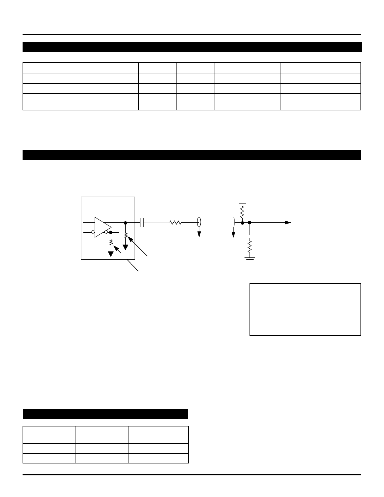
AC ELECTRICAL CHARACTERISTICS
VCC = VCCQ = VCCO = 3.0V to 5.25V
Symbol Parameter Min. Typ. Max. Unit Condition
tJIT Jitter ——10 ps RMS
PPW Duty Cycle 45% 50% 55% <500MHz
r Output Rise/Fall Time 100 300 500 ps —
t
f (20% to 80%) 100 300 500
t
APPLICATION
AC Coupled Load
VTERM = 2.5V
ClockWorks™
SY89424V
+
–
VEE = GND
VEE
CB2
RS
On chip pulldown resistor
provides 25mA (40mA at 5V
VCC) of driver current.
Z
O
Clock Interface
RR
To clock
inputs
RC
CB2 = 10nF ±20%
R
S = 6.8 Ohm ±5%
R
C = 20 Ohm ±1%
R
R = 5 KOhm ±5%
Z
O = 20 Ohm ±2 Ohm
PRODUCT ORDERING CODE
Odering Package Operating
Code Type Range
SY89424VZC Z16-1 Commercial
SY89424VZCTR Z16-1 Commercial
4
Page 5
Micrel
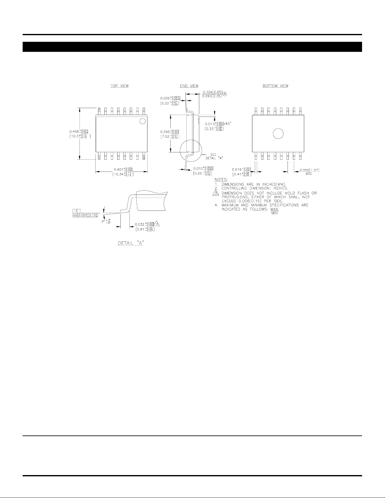
16 LEAD SOIC .300" WIDE (Z16-1)
ClockWorks™
SY89424V
Rev. 03
MICREL-SYNERGY 3250 SCOTT BOULEVARD SANTA CLARA CA 95054 USA
TEL + 1 (408) 980-9191 FAX + 1 (408) 914-7878 WEB http://www.micrel.com
This information is believed to be accurate and reliable, however no responsibility is assumed by Micrel for its use nor for any infringement of patents or
other rights of third parties resulting from its use. No license is granted by implication or otherwise under any patent or patent right of Micrel Inc.
© 2000 Micrel Incorporated
5
 Loading...