

Page 1

®
LOW VOLTAGE FAST-SWITCHING
Ordering Code Marking Shipment
STN851 N851 Tape & Reel
■ VERY LOW CO LLECT O R TO EMITTER
SATURATION VOLTAGE
■ HIGH CURRENT GAIN CHARACTE RIS TIC
■ FAST-SWITCHIN G SPE ED
■ SURFACE-MOUNTING SOT-223 MEDIUM
POWER PACKAGE IN TAPE & REEL
APPLICATIONS:
■ EMERGENCY LIGHTING
■ VOLTAG E REG UL A TO RS
■ RELAY DRIVERS
■ HIGH EFFICIE NCY LO W VO LT AGE
SWITCHING APPLICATIONS
DESCRIPTION
The device is manufactured in NPN Planar
Technology by using a "Base Island" layout.
The resulting Transistor shows exceptional high
gain performance coupled with very low
saturation voltage.
STN851
NPN POWER TRANSISTOR
PRELIMINARY DATA
2
3
2
1
SOT-223
INTERNAL SCHEMATIC DIAGRAM
ABSOL UT E MAXIMU M RATINGS
Symbol Parameter Value Unit
V
V
V
I
I
P
T
September 2003
Collector-Base Voltage (IE = 0) 150 V
CBO
Collector-Emitter Voltage (IB = 0) 60 V
CEO
Emitter-Base Voltage (IC = 0) 7 V
EBO
I
Collector Current 5 A
C
Collector Peak Current (tp < 5 ms) 10 A
CM
I
Base Current 1 A
B
Base Peak Current (tp < 5 ms) 2 A
BM
Total Dissipation at T
tot
Storage Temperature -65 to 150
stg
T
Max. Operating Junction Temperature 150
j
= 25 oC 1.6 W
amb
o
C
o
C
1/7
Page 2
STN851
THERMAL DATA
R
thj-amb
• Device mo unte d on a P.C.B . ar ea of 1 cm
Thermal Resistance Junction-ambient Max 78
o
2
C/W
ELECTRICAL CHARACTERISTICS (T
= 25 oC unless otherwise specified)
case
Symbol Parameter Test Conditions Min. Typ. Max. Unit
I
CBO
I
EBO
V
(BR)CBO
Collector Cut-off
Current (I
= 0)
E
Emitter Cut-off Current
(I
= 0)
C
Collector-Base
= 120 V
V
CB
V
= 120 V Tj = 100 oC
CB
= 7 V 10 nA
V
EB
= 100 µA
I
C
150 V
50
1
Breakdown Voltage
(I
= 0)
E
V
(BR)CEO
∗ Collector-Emitter
I
= 10 mA 60 V
C
Breakdown Voltage
(I
= 0)
B
V
(BR)EBO
Emitter-Base
= 100 µA
I
E
7V
Breakdown Voltage
(I
= 0)
C
V
∗ Collector-Emitter
CE(sat)
Saturation Voltage
V
∗ Base-Emitter
BE(sat)
IC = 100 mA IB = 5 mA
I
= 1 A IB = 50 mA
C
I
= 2 A IB = 50 mA
C
I
= 5 A IB = 200 mA
C
10
70
140
320
IC = 4 A IB = 200 mA 1 1.15 V
50
120
250
500
Saturation Voltage
∗ Base-Emitter On
V
BE(on)
IC = 4 A VCE = 1 V 0.89 1 V
Voltage
∗ DC Current Gain IC = 10 mA VCE = 1 V
h
FE
f
C
CBO
Transition frequency V
T
Collector-Base
I
= 2 A VCE = 1 V
C
I
= 5 A VCE = 1 V
C
I
= 10 A VCE = 1 V
C
= 10 V IC = 100 mA 130 MHz
CE
VCB = 10 V f = 1 MHz 50 pF
150
150
90
30
300
270
140
50
350
Capacitance
RESISTIVE LOAD
on
s
t
f
Turn- on Time
Storage Time
Fall Time
t
t
* Pulsed: Pulse duration = 300µs, duty cycle = 1.5 %
I
= 1 A VCC = 10 V
C
I
= - IB2 = 0.1 A
B1
50
1.35
120
nA
µA
mV
mV
mV
mV
ns
µs
ns
2/7
Page 3
STN851
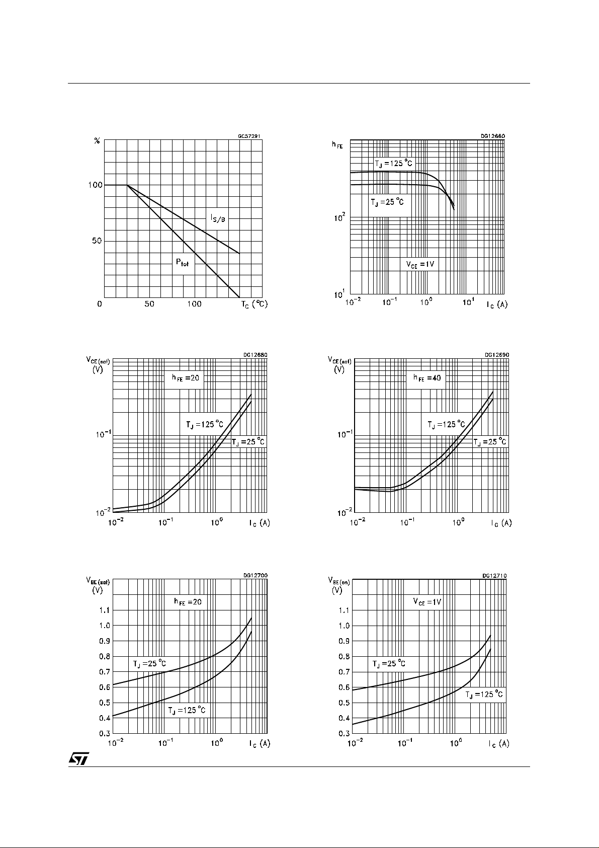
Derating Curve
DC Current Gain
Collector-Em itter Sat uration Volt ag e Collector-Emitter Saturation Voltage
Base-Emitter Saturation Voltage Base-Emitter On Voltage
3/7
Page 4

STN851
Switching Times Resistive Load
Switching Times Resistive Load
Switching Times Resistive Load
Switching Times Inductive Load
Switching Times Inductive Load
4/7
Page 5

Figure 1: Resistive Load Switching Test Circuit.
1) Fast electronic switch
2) Non-inductive Resistor
STN851
5/7
Page 6

STN851
SOT-223 MECHANICAL DATA
DIM.
MIN. TYP. MAX. MIN. TYP. MAX.
A 1.80 0.071
B 0.60 0.70 0.80 0.024 0.027 0.031
B1 2.90 3.00 3.10 0.114 0.118 0.122
c 0.24 0.26 0.32 0.009 0.010 0.013
D 6.30 6.50 6.70 0.248 0.256 0.264
e 2.30 0.090
e1 4.60 0.181
E 3.30 3.50 3.70 0.130 0.138 0.146
H 6.70 7.00 7.30 0.264 0.276 0.287
V10
A1 0.02
mm inch
o
10
o
6/7
P008B
Page 7

STN851
Information furnished is believed to be accurate and reliable. However, STMicroelectronics assumes no responsibility for the consequences
of use of such inform ation nor for any infringe ment o f patents or other rig hts o f third par ties which ma y resul t from i ts use. N o li cen se is
granted by implicatio n or otherwise under any patent or patent rights of STMicroelectronics. Specification mentioned in this publication are
subject to change without notice. This publication supersedes and replaces all information previously supplied. STMicroelectronics products
are not authorized for use as critical compo nents in life support devices or systems without express written approval of STMicroelectronics.
The ST logo is a trademark of STMicroelectronics.
All other names are the property of their respective owners.
© 2003 STMicroelectronics – All Rights reserved
STMicroelectronics GROUP OF COMPANIES
Australia - Belgium - Brazil - Canada - China - Czech Republic - Finland - France - Germany - Hong Kong - India - Israel - Italy - Japan -
Malaysia - Malta - Morocco - Singapore - Spain - Sweden - Switzerland - United Kingdom - United States.
http://www.st.com
7/7
 Loading...