

Page 1
STN7NF10
N-CHANNEL 100V - 0.055 Ω -5ASOT-223
LOW GATE CHARGE STripFET™ II POWER MOSFET
TYPE V
STN7NF10 100 V < 0.065 Ω 5A
■ TYPICAL R
■ APPLICATION ORIENTED
DS
DSS
(on) = 0.055 Ω
R
DS(on)
I
D
CHARACTERIZATION
DESCRIPTION
This Power MOSF ET s eries realized with STMicroelectronics uniqueSTripFET proces s hasspecifically been designed to minimize input capacitance and
gate charge. It is therefore suitable as primary
switch in advanced high-efficiency isolated DC-DC
converters f or Telecom and Computer application. It
is also intended for any application with low gate
charge drive requirements.
APPLICATIONS
■ HIGH-EFFICIENCY DC-DC CONVERTERS
■ UPS AND MOTOR CONTROL
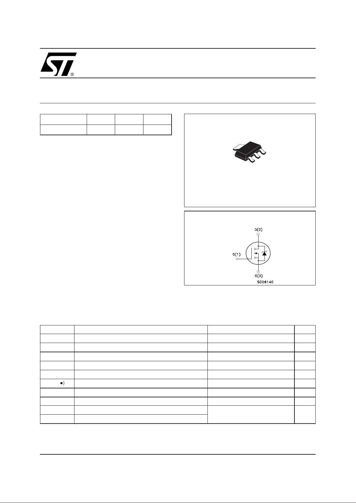
2
3
2
1
SOT-223
INTERNAL SCHEMATIC DIAGRAM
ABSOLUTE MAXIMUM RATINGS
Symbol Parameter Value Unit
V
DS
V
DGR
V
GS
I
D
I
D
I
DM
P
TOT
T
stg
T
j
(●) Pulse width limited by safe operating area
Drain-source Voltage (VGS=0)
Drain-gate Voltage (RGS=20kΩ)
Gate- source Voltage ±20 V
Drain Current (continuous) at TC= 25°C
Drain Current (continuous) at TC= 100°C
()
Drain Current (pulsed) 20 A
Total Dissipation at TC= 25°C
Derating Factor 0.026 W/°C
Storage Temperature
Operating Junction Temperature
100 V
100 V
5A
3.4 A
3.3 W
–55 to 150 °C
1/8December 2002
Page 2

STN7NF10
THERMAL DATA
Rthj-PCB Thermal Resistance Junction-PCB Max(*) 38 °C/W
Rthj-PCB Thermal Resistance Junction-PCB Max(**) 100 °C/W
T
l
Note: (*) When mounted on 1 in2FR-4 BOARD,2 oz Cu, t<10s.
Note: (**) When mounted on minimum footprint.
Maximum Lead Temperature For Soldering Purpose
(1.6 mm from case,for 10s)
260 °C
ELECTRICAL CHARACTERISTICS (T
= 25 °C UNLESS OTHERWISE SPECIFIED)
CASE
OFF
Symbol Parameter Test Conditions Min. Typ. Max. Unit
V
(BR)DSS
Drain-source
ID= 250 µA, VGS= 0 100 V
Breakdown Voltage
I
DSS
I
GSS
Zero Gate Voltage
Drain Current (V
GS
Gate-body Leakage
Current (V
DS
=0)
=0)
V
= Max Rating
DS
= Max Rating, TC= 125 °C
V
DS
V
= ±20V ±100 nA
GS
10 µA
1µA
ON (1)
Symbol Parameter Test Conditions Min. Typ. Max. Unit
V
GS(th)
R
DS(on)
Gate Threshold Voltage
Static Drain-source On
V
DS=VGS,ID
VGS=10V,ID= 1.5 A
= 250µA
234V
0.055 0.065 Ω
Resistance
DYNAMIC
Symbol Parameter Test Conditions Min. Typ. Max. Unit
(1) Forward Transconductance VDS=15V,ID=1.5A 12 S
g
fs
C
iss
C
oss
C
rss
Input Capacitance
Output Capacitance 125 pF
Reverse Transfer
Capacitance
V
=25V,f=1MHz,VGS=0
DS
870 pF
52 pF
2/8
Page 3
STN7NF10
ELECTRICAL CHARACTERISTICS (CONTINUED)
SWITCHING ON
Symbol Parameter Test Conditions Min. Typ. Max. Unit
V
t
d(on)
Q
Q
Q
t
r
g
gs
gd
Turn-on Delay Time
Rise Time 45 ns
Total Gate Charge
Gate-Source Charge
Gate-Drain Charge
SWITCHING OFF
Symbol Parameter Test Conditions Min. Typ. Max. Unit
t
d(off)
t
f
Turn-off-Delay Time
Fall Time
SOURCE DRAIN DIODE
Symbol Parameter Test Conditions Min. Typ. Max. Unit
I
SD
I
SDM
VSD(2)
t
rr
Q
rr
I
RRM
Note: 1. Pulsed: Pulse duration = 300 µs, duty cycle 1.5 %.
2. Pulse width limited by safe operating area.
Source-drain Current 5 A
(1)
Source-drain Current (pulsed) 20 A
Forward On Voltage
Reverse Recovery Time
Reverse Recovery Charge
Reverse Recovery Current
=50V,ID=12A
DD
= 4.7Ω VGS=10V
R
G
(see test circuit, Figure 3)
VDD=80V,ID=24A,
V
=10V
GS
VDD=50V,ID=12A,
RG=4.7Ω, VGS= 10V
(see test circuit, Figure 3)
ISD= 5 A, VGS=0
= 5 A, di/dt = 100A/µs,
I
SD
VDD=30V,Tj= 150°C
(see test circuit, Figure 5)
58 ns
30
41 nC
6
10
49
17
1.3 V
100
375
7.5
nC
nC
ns
ns
ns
nC
A
3/8
Page 4

STN7NF10
Thermal Impede nceSafe Operating Area
Output Characteristics Transfer Characteristics
Transconductance Static Drain-source On Resistance
4/8
Page 5

Gate Charge vs Gate-source Voltage Capacitance Variations
Normalized On Resistance vs TemperatureNormalized Gate Thereshold Voltage vs Temp.
STN7NF10
Source-drain Diode Forward Characteristics
5/8
Page 6

STN7NF10
Fig. 2: Unclamped Inductive WaveformFig. 1: Unclamped Inductive Load Test Circuit
Fig. 3: Switching Times Test Circuit For
Resistive Load
Fig. 5: Test Circuit For Inductive Load Switching
And Diode Recovery Times
Fig. 4: Gate Charge test Circuit
6/8
Page 7

SOT-223 MECHANICAL DATA
STN7NF10
DIM.
MIN. TYP. MAX. MIN. TYP. MAX.
A 1.80 0.071
B 0.60 0.70 0.80 0.024 0.027 0.031
B1 2.90 3.00 3.10 0.114 0.118 0.122
c 0.24 0.26 0.32 0.009 0.010 0.013
D 6.30 6.50 6.70 0.248 0.256 0.264
e 2.30 0.090
e1 4.60 0.181
E 3.30 3.50 3.70 0.130 0.138 0.146
H 6.70 7.00 7.30 0.264 0.276 0.287
V10
A1 0.02
mm inch
o
10
o
P008B
7/8
Page 8

STN7NF10
Information furnished is believed to be accurate and reliable. However, STMicroelectronics assumes no responsibility f or the
consequences of use of su ch in formation nor for any in fringement of paten ts or o ther rights of third parties w hich may result from
its use. No license is granted by implication or otherwise under any patent or patent rights of STMicroelectronics. Specifications
mentioned in this publication are subject to change without notice. This publication supersedes and replaces all information
previously suppli ed. STMi croelect ronics pr oducts are not author ized for use as c ritical component s in li fe suppo rt devi ces or
systems without express written approval of STMicroelectronics.
Australia - Brazil - Canada - China - Finland - France - Germany - Hong Kong - India - Israel - Italy - Japan - Malaysia - Malta - Morocco
© The ST logo is a registered trademark of STMicroelectronics
© 2002 STMicroelectronics - Printed in Italy - All Rights Reserved
Singapore - Spain - Sweden - Switzerland - United Kingdom - United States.
STMicroelectronics GROUP OF COMPANIES
© http://www.st.com
8/8
 Loading...