

Page 1
®
MEDIUM CURRENT, HIGH PERFORMANCE,
LOW VOLTAGE PNP TRANSISTOR
Ordering Code Marking
STN749 N749
■ VERY LOW CO LLECT O R TO EMITTER
SATURATION VOLTAGE
■ DC CURRENT GAIN, h
■ 3 A CONTINUOUS COLLECTOR CURRENT
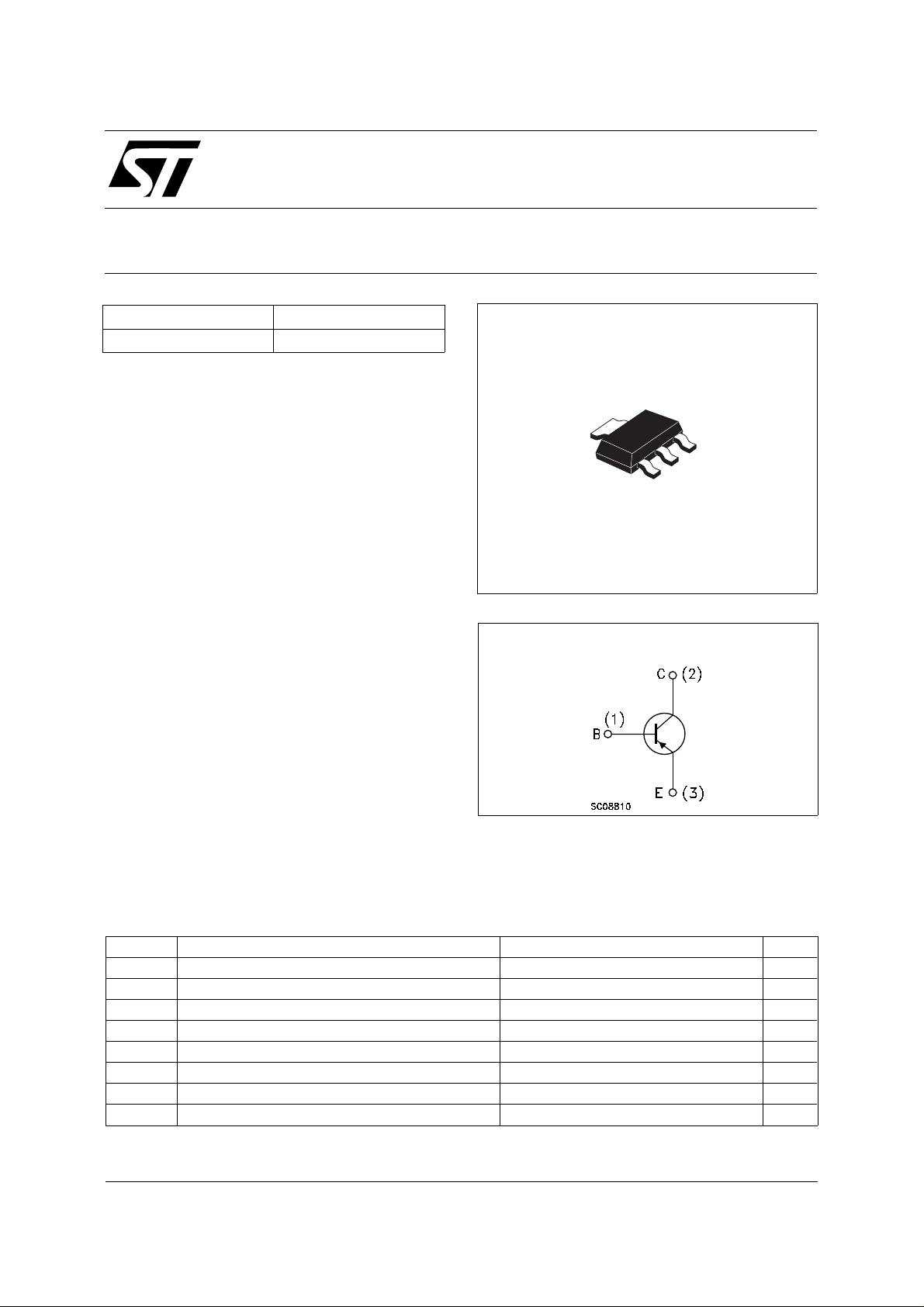
■ SOT-223 PLASTIC PAC KA GE FOR
SURFACE MOUNTING CIRCUITS
■ AVAILABLE IN TAPE AND REEL PACKING
> 100
FE
STN749
2
3
2
1
APPLICATIONS
■ POWER MANAGEMENT IN PORTABLE
SOT-223
EQUIPMENT
■ VOLTAGE REGULATION IN BIAS SUPPLY
CIRCUITS
■ SWITCHING RE G ULATOR IN BATTER Y
CHARGER APPLICATIONS
■ HEAVY LOAD DRIVER
INTER NAL SCH E M ATI C DIAG RA M
DESCRIPTION
The device is manufactured in low voltage PNP
Planar Technology by using a "Base Island"
layout.
The resulting Transistor shows exceptional high
gain performance coupled with very low
saturation voltage.
ABSOLUTE MAXIMUM RATINGS
Symbol Parameter Value Unit
V
V
V
I
P
T
Collector-Base Voltage (IE = 0) -35 V
CBO
Collector-Emitter Voltage (IB = 0) -25 V
CEO
Emitter-Base Voltage (IC = 0) -5 V
EBO
Collector Current -3 A
I
C
Collector Peak Current (tp < 5 ms) -6 A
CM
Total Dissipation at T
tot
Storage Temperature -65 to 150
stg
Max. Operating Junction Temperature 150
T
j
= 25 oC 1.6 W
amb
o
C
o
C
March 2003
1/6
Page 2
STN749
THERMAL DATA
R
• Thermal Resistance Junction-Ambient Max 78
thj-amb
• Device mounted on a PCB area of 1 cm2 .
o
C/W
ELECTRICAL CHARACTERISTICS (T
= 25 oC unless otherwise specified)
case
Symbol Parameter Test Conditions Min. Typ. Max. Unit
I
CBO
I
EBO
V
(BR)CEO
Collector Cut-off
Current (I
= 0)
E
Emitter Cut-off Current
(I
= 0)
C
∗ Collector-Emitter
= -30 V
V
CB
V
= -30 V Tj = 100 oC
CB
= -4 V -100 nA
V
EB
I
= -10 mA -25 V
C
-100
-10
Breakdown Voltage
(I
= 0)
B
V
(BR)CBO
Collector-Base
= -100 µA
I
C
-35 V
Breakdown Voltage
(I
= 0)
E
V
(BR)EBO
Emitter-Base
= -100 µA
I
E
-5 V
Breakdown Voltage
(I
= 0)
C
V
CE(sat)
V
BE(sat)
∗ Collector-Emitter
Saturation Voltage
∗ Base-Emitter
IC = -1A IB = -100 mA
I
= -3A IB = -300 mA
C
-0.3
-0.6
IC = -1 A IB = -100 mA -1.25 V
Saturation Voltage
V
BE(on)
Base-Emitter Turn-On
IC = -1 A VCE = -2 V -1 V
Voltage
∗ DC Current Gain IC = -50 mA VCE = -2 V
h
FE
∗ Pulsed: Pulse duration = 300 µs, duty cycle ≤ 1.5 %
I
= -1 A VCE = -2 V
C
I
= -2 A VCE = -2 V
C
I
= -6 A VCE = -2V
C
70
100
75
15
300
nA
µA
V
V
2/6
Page 3

STN749
DC Current Gain
DC Current Gain
Collector -Em it ter Sat uration V oltage Base-Emitt er Sat uration Volta ge
Switching Times Resis tive Load Switching Times Resist ive Load
3/6
Page 4

STN749
Figure 1: Resistive Load Switching Test Circuit.
1) Fast electronic switch
2) Non-inductive Resistor
4/6
Page 5

SOT-223 MECHANICAL DATA
STN749
DIM.
MIN. TYP. MAX. MIN. TYP. MAX.
A 1.80 0.071
B 0.60 0.70 0.80 0.024 0.027 0.031
B1 2.90 3.00 3.10 0.114 0.118 0.122
c 0.24 0.26 0.32 0.009 0.010 0.013
D 6.30 6.50 6.70 0.248 0.256 0.264
e 2.3 0 0.090
e1 4.60 0.181
E 3.30 3.50 3.70 0.130 0.138 0.146
H 6.70 7.00 7.30 0.264 0.276 0.287
V10
A1 0.02
mm inch
o
10
o
P008B
5/6
Page 6

STN749
Information furnished is believed to be accurate and reliable. However, STMicroelectronics assumes no responsibility for the consequences
of use of such inform ation nor for any infringe ment o f patents or other rig hts o f third par ties which ma y resul t from i ts use. N o li cen se is
granted by implicatio n or otherwise under any patent or patent rights of STMicroelectronics. Specification mentioned in this publication are
subject to change without notice. This publication supersedes and replaces all information previously supplied. STMicroelectronics products
are not authorized for use as critical compo nents in life support devices or systems without express written approval of STMicroelectronics.
The ST logo is a trademark of STMicroelectronics
© 2003 STMicroelectro nics – Printed in Italy – All Rights Reserved
STMicroelectronics GROUP OF COMPANIES
Australia - Brazil - Canada - China - Finland - France - Germany - Hong Kong - India - Israel - Italy - Japan - Malaysia - Malta - Morocco -
Singapore - Spain - Sweden - Switzerland - United Kingdom - United States.
http://www.st.com
6/6
 Loading...