

Page 1
STN4NF03L
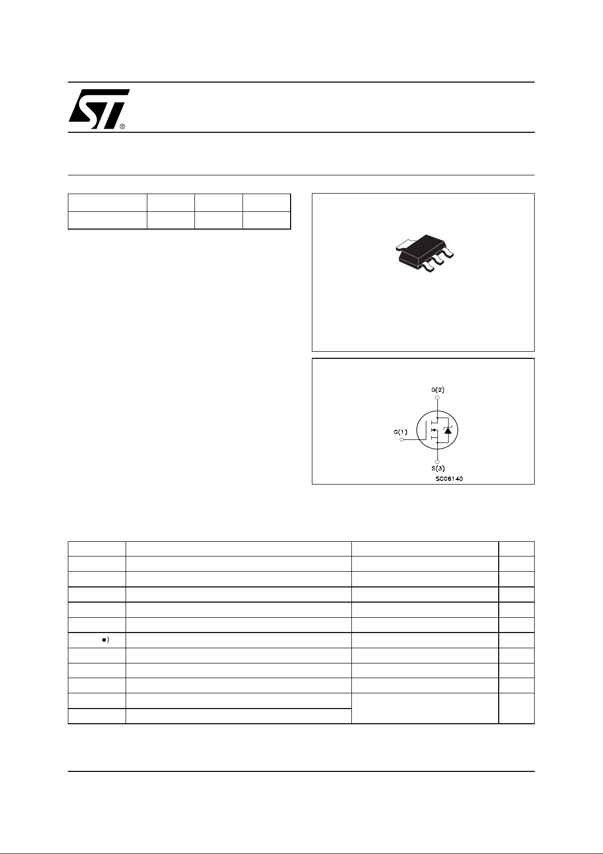
N-CHANNEL 30V - 0.039Ω -6.5ASOT-223
STripFET™ II POWER M OSFET
TYPE V
DSS
R
DS(on)
I
D
STN4NF03L 30V <0.05Ω 6.5A
■ TYPICAL R
■ LOW T HRE S HOLD DRIVE
(on) = 0.039Ω
DS
DESCRIPTION
This Power Mosfet is the latest development of STMicroelectronics unique “Single Feature Size™
” strip-
based process. The resulting transistor shows extremely high packing d ens ity for low on-resistance,
rugged avalance characteristics and less critical alignment steps therefore a remarkable manufacturing reproducibility.
APPLICATIONS
■ DC-DC & DC-AC CONVERTERS
■ DC MOTO R CONTROL (DISK DRIVES, etc.)
■ SYNCHRONOUS RECTIFICATION
2
3
2
1
SOT-223
INTERNAL SCHE M ATIC DIAGRAM
ABSOLUTE MAX IMUM RATINGS
Symbol Parameter Value Unit
V
DS
V
DGR
V
GS
I
D
I
D
I
DM
P
TOT
E
AS
T
stg
T
j
(●) Pulse width limited by safe operating area
Drain-source Voltage (VGS=0)
Drain-gate Voltage (RGS=20kΩ)
30 V
30 V
Gate- source Voltage ±16 V
Drain Current (continuous) at TC= 25°C
Drain Current (continuous) at TC= 100°C
()
Drain Current (pulsed) 26 A
Total Dissipation at TC= 25°C
6.5 A
4.5 A
3.3 W
Derating Factor 0.026 W/°C
(1)
Single Pulse Avalanche Energy 200 mJ
Storage Temperature
Operating Junction Temperature
(1) Starting Tj=25°C, ID=6.5A, VDD=15V
–55 to 175 °C
1/8December 2002
Page 2
STN4NF03L
THERMAL DATA
Rthj-PCB Thermal Resistance Junction-PC Board Max (*) 38 °C/W
Rthj-PCB Thermal Resistance Junction-PCB Max (**) 100 °C/W
T
l
Note: (*) When mounted on 1 in2FR-4 board , 2 oz Cu, t<10s.
Note: (**) Minimum recommended footprint
Maximum Lead Temperature For Soldering Purpose
(1.6 mm from case for 10s)
260 °C
ELECTRICAL CHARACTE RISTICS (T
= 25 °C UNLESS OTHERWISE SPECIFIED)
CASE
OFF
Symbol Parameter Test Conditions Min. Typ. Max. Unit
V
(BR)DSS
Drain-source
ID= 250 µA, VGS= 0 30 V
Breakdown Voltage
I
DSS
I
GSS
Zero Gate Voltage
Drain Current (V
GS
Gate-body Leakage
Current (V
DS
=0)
=0)
V
= Max Rating
DS
= Max Rating, TC= 125 °C
V
DS
V
= ±16V ±100 nA
GS
10 µA
1µA
ON (1)
Symbol Parameter Test Conditions Min. Typ. Max. Unit
V
GS(th)
R
DS(on)
Gate Threshold Voltage
Static Drain-source On
Resistance
V
DS=VGS,ID
=10V,ID=2A
V
GS
=5V,ID=2A
V
GS
= 250 µA
1V
0.039 0.05 Ω
0.046 0.06 Ω
DYNAMIC
Symbol Parameter Test Conditions Min. Typ. Max. Unit
(1)
g
fs
C
iss
C
oss
C
rss
Forward Transconductance
Input Capacitance
Output Capacitance 90 pF
Reverse Transfer
Capacitance
VDS=10V,ID=2 A
V
=25V,f=1MHz,VGS=0
DS
13 S
330 pF
40 pF
2/8
Page 3

STN4NF03L
ELECTRICAL CHARACTE RISTICS (CONTINUED)
SWITCHING ON
Symbol Parameter Test Conditions Min. Typ. Max. Unit
t
d(on)
Q
Q
Q
t
r
g
gs
gd
Turn-on Delay Time VDD=15V,ID=2A
= 4.7Ω VGS=4.5V
R
Rise Time 100 ns
Total Gate Charge
Gate-Source Charge
Gate-Drain Charge
G
(see test circuit, Figure 3)
VDD=24V,ID=4A,
V
=10V
GS
SWITCHING OFF
Symbol Parameter Test Conditions Min. Typ. Max. Unit
t
d(off)
Turn-off-Delay Time VDD=15V,ID=2A,
RG=4.7Ω, VGS= 4.5 V
(see test circuit, Figure 3)
t
f
Fall Time 22 ns
SOURCE DRAIN DIODE
Symbol Parameter Test Conditions Min. Typ. Max. Unit
I
SD
I
SDM
V
SD
t
rr
Q
rr
I
RRM
Note: 1. Pulsed: Pulse duration = 300 µs, duty cycle 1.5 %.
2. Pulse width limited by safe operating area.
Source-drain Current
(2)
Source-drain Current (pulsed)
(1)
Forward On Voltage
Reverse Recovery Time
Reverse Recovery Charge
Reverse Recovery Current
ISD= 6.5 A, VGS=0
= 6.5 A, di/dt = 100 A/µs,
I
SD
VDD=15V,Tj= 150°C
(see test circuit, Figure 5)
11 ns
6.5
9nC
3.6
2
25 ns
6.5
26
1.5 V
35
25
1.4
nC
nC
A
A
ns
nC
A
Safe Operating Area
Thermal Impedence Junction-PCB
3/8
Page 4

STN4NF03L
Output Characteristics
Transconductance
Transfer Characteristics
Static Drain-source On Resistance
Gate Charge vs Gate-so urc e Voltage Capac itance Variations
4/8
Page 5

STN4NF03L
Normalized GateThereshold Voltage vs Temp. Normalized On Resistance vs Temperature
Source-drain Diode Forward Characteristics
5/8
Page 6

STN4NF03L
Fig. 2: Unclamped Inductive WaveformFig. 1: Unclamped Inductive Loa d Test Circuit
Fig. 3: Switching Times Test Circuit For
Resistive Load
Fig. 5: Test Circuit For Inductive Load Switching
And Diode Recovery Times
Fig. 4: Gate Charge test Circuit
6/8
Page 7

P008B
SOT-223 MECHANICAL DATA
STN4NF03L
DIM.
MIN. TYP. MAX. MIN. TYP. MAX.
A 1.80 0.071
B 0.60 0.70 0.80 0.024 0.027 0.031
B1 2.90 3.00 3.10 0.114 0.118 0.122
c 0.24 0.26 0.32 0.009 0.010 0.013
D 6.30 6.50 6.70 0.248 0.256 0.264
e 2.30 0.090
e1 4.60 0.181
E 3.30 3.50 3.70 0.130 0.138 0.146
H 6.70 7.00 7.30 0.264 0.276 0.287
V10
A1 0.02
mm inch
o
10
o
7/8
Page 8

STN4NF03L
Information furnished is believed to be accurate and reliable. However, STMicroelectronics assumes no responsibility for the
consequences of u se of such inf ormat ion nor for any in fring ement of p aten ts or othe r ri ghts of th ird p arties whic h may resul t f rom
its use. No license is granted by implication or otherwise under any patent or patent rights of STMicroelectronics. Specifications
mentioned in this publication are subject to change without notice. This publication supersedes and replaces all information
previously supplied. STMicroelectronics products are not authorized for use as critical components in life support devices or
systems without express written approval of STMicroelectronics.
Australia - Brazil - Canada - China - Finland - France - Germany - Hong Kong - India - Israel - Italy - Japan - Malaysia - Malta - Morocco
© The ST logo is a registered trademark of STMicroelectronics
© 2003 STMicroelectronics - Printed in Italy - All Rights Reserved
Singapore - Spain - Sweden - Switzerland - United Kingdom - United States.
STMicroelectronics GROUP OF COMPANIES
© http://www.st.com
8/8
 Loading...