

Page 1
STN4NE03
N - CHANNEL 30V - 0.045Ω - 4A - SOT-223
STripFET POWER MOSFET
TYPE V
DSS
R
DS(on)
I
D
STN4N E03 30 V < 0.06 Ω 4A
■ TYPICALR
■ EXCEPTIONALdv/dt CAPABILITY
■ AVALANCHERUGGEDTECHNOLOGY
■ 100% AVALANCHETESTED
■ APPLICATIONORIENTED
DS(on)
=0.045 Ω
CHARACTERIZATION
DESCRIPTION
This Power MOSFET is the latestdevelopmentof
STMicroelectronics unique ” Single Feature
”
Size
strip-based process. The resulting
transistor shows extremely high packing density
for low on-resistance, rugged avalanche
characteristics and less critical alignment steps
therefore a remarkable manufacturing
reproducibility.
APPLICATIONS
■ DC MOTOR CONTROL (DISK DRIVES, etc.)
■ DC-DC& DC-AC CONVERTERS
■ SYNCHRONOUSRECTIFICATION
■ POWERMANAGEMENT IN
BATTERY-OPERATEDAND PORTABLE
EQUIPMENT
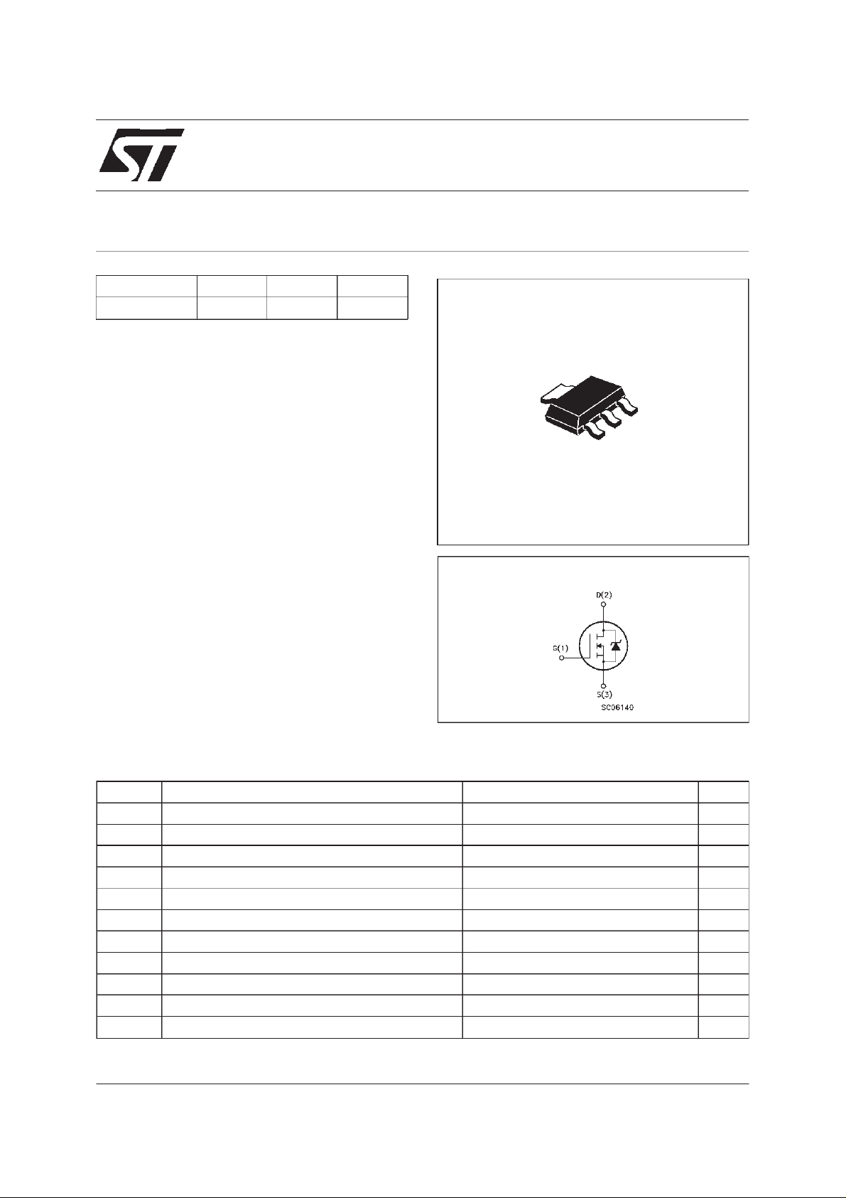
2
3
2
1
SOT-223
INTERNAL SCHEMATIC DIAGRAM
ABSOLUTE MAXIMUM RATINGS
Symbol Parameter Value Unit
V
V
DGR
V
I
D
I
D
I
DM
P
dv/dt (
T
(•) Pulse width limited by safe operating area (*) Limited by package (1)ISD≤ 10A, di/dt ≤ 300A/µs, VDD≤ V
August 1998
Drain-s ou r ce Voltage (VGS=0) 30 V
DS
Drain- gat e Volt ag e (RGS=20kΩ)
Gate-source Vol tage ± 20 V
GS
30 V
(*) Drain Cur r en t (continu ous) at Tc=25oC4A
(*) Drain Cur r en t (continu ous) at Tc=100oC2.5A
(•) Dr ain Curren t ( p ulsed) 16 A
Tot al Di s sipa t ion at Tc=25oC2.5W
tot
Derat ing Factor 0.02 W/
1) Peak Diode Recovery volta ge slope 6 V/ns
Storage Temperature -65 to 150
stg
T
Max. Oper ating Jun ct io n T e m pe r ature 150
j
(BR)DSS
,Tj≤T
o
C
o
C
o
C
jMAX
1/8
Page 2
STN4NE03
THERMAL DATA
R
thj-pcb
R
thj- amb
T
AVALANCHE CHARACTERISTICS
Symbol Para met e r Max Valu e Uni t
I
AR
E
Ther mal Resist ance Junctio n- PC Board Max
Ther mal Resist ance Junctio n- ambient Max
(Sur f a ce M ounted)
Maximum Lead Tempera t ure For Soldering P urpose
l
Avalanch e C urr e nt , Repetit i v e o r Not-Re petitiv e
(pulse w idth limited by T
Single Pulse Avalanche Energy
AS
(starting T
=25oC, ID=IAR,VDD=25V)
j
max, δ <1%)
j
50
60
260
4A
20 mJ
o
C/W
o
C/W
o
C
ELECTRICAL CHARACTERISTICS (T
=25oC unlessotherwisespecified)
case
OFF
Symbol Parameter Test Condition s Min. Typ. Max. Unit
V
(BR)DSS
Drain-sou rc e
=250µAVGS=0
I
D
30 V
Breakdown Voltage
I
I
DSS
GSS
Zer o Gat e Voltage
Drain Current (V
GS
Gat e-body Le aka ge
Current (V
DS
=0)
=0)
=MaxRating
V
DS
V
=MaxRating Tc=125
DS
o
C
= ± 20 V
V
GS
1
10
± 100 nA
ON (∗)
Symbol Parameter Test Condition s Min. Typ. Max. Unit
V
GS(th )
Gate Threshold
V
DS=VGSID
=250µA
234V
Voltage
R
DS(on)
Stati c Drain-so urce On
VGS=10V ID= 2 A 0.045 0. 0 6 Ω
Resistance
I
D(on)
On Stat e Drain Current VDS>I
D(on)xRDS(on)max
4A
VGS=10V
DYNAMIC
Symbol Parameter Test Condition s Min. Typ. Max. Unit
g
(∗)Forward
fs
Tr anscond uctanc e
C
C
C
Input Ca paci t ance
iss
Out put C apa c itanc e
oss
Reverse Trans fer
rss
Capa cit an c e
VDS>I
D(on)xRDS(on)maxID
=2A 1 3.0 S
VDS=25V f=1MHz VGS= 0 V 760
150
50
1000
200
80
µA
µA
pF
pF
pF
2/8
Page 3
STN4NE03
ELECTRICAL CHARACTERISTICS (continued)
SWITCHINGON
Symbol Parameter Test Condition s Min. Typ. Max. Unit
t
d(on)
t
r
Turn-on Time
Rise Time
VDD=5V ID=5A
=4.7 Ω VGS=10V
R
G
10
60
(see test circuit, figure 3)
Q
Q
Q
Total Gate Charge
g
Gat e-Sou r ce Cha rge
gs
Gate-Drain Charge
gd
VDD=24V ID=10A VGS=10V 22
7
7
SWITCHINGOFF
Symbol Parameter Test Condition s Min. Typ. Max. Unit
t
r(Voff)
t
t
Of f - voltag e Rise Time
Fall Time
f
Cross-over Time
c
VDD=24V ID=10A
=4.7 Ω VGS=10V
R
G
(see test circuit, figure 5)
8
15
25
SOURCE DRAIN DIODE
Symbol Parameter Test Condition s Min. Typ. Max. Unit
I
SD
I
SDM
V
SD
t
Q
I
RRM
(∗) Pulsed: Pulse duration =300 µs, duty cycle1.5 %
(•) Pulse widthlimited by safe operating area
Source-drain Curre nt
(•)
Source-drain Curre nt
(pulsed)
(∗) Fo rward On Vo lt age ISD=4A VGS=0 1.5 V
Reverse Rec overy
rr
Time
Reverse Rec overy
rr
= 10 A di/dt = 100 A/µs
I
SD
=24V Tj=150oC
V
DD
(see test circuit, figure 5)
40
0.06
Charge
Reverse Rec overy
3.0
Current
15
90
30 nC
15
25
40
4
16
ns
ns
nC
nC
ns
ns
ns
A
A
ns
µC
A
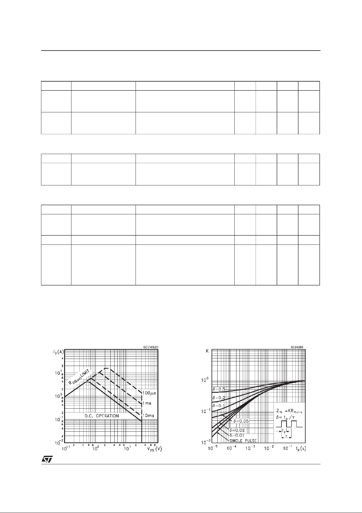
Safe Operating Area ThermalImpedance
3/8
Page 4

STN4NE03
OutputCharacteristics
Transconductance
TransferCharacteristics
StaticDrain-sourceOn Resistance
GateCharge vs Gate-sourceVoltage
4/8
CapacitanceVariations
Page 5

STN4NE03
Normalized GateThresholdVoltagevs
Temperature
Source-drainDiode Forward Characteristics
Normalized On Resistancevs Temperature
5/8
Page 6

STN4NE03
Fig. 1: UnclampedInductiveLoad Test Circuit
Fig. 3: Switching Times Test CircuitsFor
ResistiveLoad
Fig. 2: UnclampedInductive Waveform
Fig. 4: Gate Charge test Circuit
Fig. 5: Test Circuit For Inductive Load Switching
And Diode RecoveryTimes
6/8
Page 7

SOT-223 MECHANICAL DATA
STN4NE03
DIM.
mm mils
MIN. TYP. MAX. MIN. TYP. MAX.
a 2.27 2.3 2.33 89.4 90.6 91.7
b 4.57 4.6 4.63 179.9 181.1 182.3
c 0.2 0.4 0.6 7.9 15.7 23.6
d 0.63 0.65 0.67 24.8 25.6 26.4
e1 1.5 1.6 1.7 59.1 63 66.9
e4 0.32 12.6
f 2.9 3 3.1 114.2 118.1 122.1
g 0.67 0.7 0.73 26.4 27.6 28.7
l1 6.7 7 7.3 263.8 275.6 287.4
l2 3.5 3.5 3.7 137.8 137.8 145.7
L 6.3 6.5 6.7 248 255.9 263.8
L
l2
e1
a
b
d
c
e4
f
C
l1
B
C
E
g
P008B
7/8
Page 8

STN4NE03
Information furnished is believed to beaccurate and reliable. However, STMicroelectronics assumes no responsibility forthe consequences
of use of such information nor for any infringement of patents or other rights of third parties which may result from its use. No license is
granted by implication orotherwise under any patent or patent rights ofSTMicroelectronics. Specification mentioned in this publication are
subject to change without notice. This publication supersedes andreplaces all information previously supplied. STMicroelectronics products
are not authorized for use as critical components in life support devices or systems without express written approval of STMicroelectronics.
The ST logo is a registered trademark of STMicroelectronics
1998 STMicroelectronics –Printed inItaly – All RightsReserved
STMicroelectronics GROUP OF COMPANIES
Australia - Brazil -Canada -China - France - Germany - Italy - Japan - Korea -Malaysia - Malta - Mexico- Morocco - TheNetherlands -
8/8
Singapore - Spain - Sweden - Switzerland- Taiwan - Thailand -United Kingdom - U.S.A.
.
 Loading...