

Page 1
STGB3NB60HD
N-CHANNEL 3A - 600V TO-263
PowerMESH IGBT
TYPE V
CES
V
CE(sat)
I
C
ST G B3NB60HD 600 V < 2. 8 V 3 A
■ HIGHINPUT IMPEDANCE
(VOLTAGEDRIVEN)
■ LOW ON-VOLTAGEDROP (V
■ LOW GATECHARGE
■ HIGHCURRENTCAPABILITY
■ VERYHIGH FREQUENCYOPERATION
■ OFFLOSSES INCLUDETAIL CURRENT
■ CO-PACKAGEDWITH TURBOSWITCH
ANTIPARALLELDIODE
■ SURFACE-MOUNTINGD
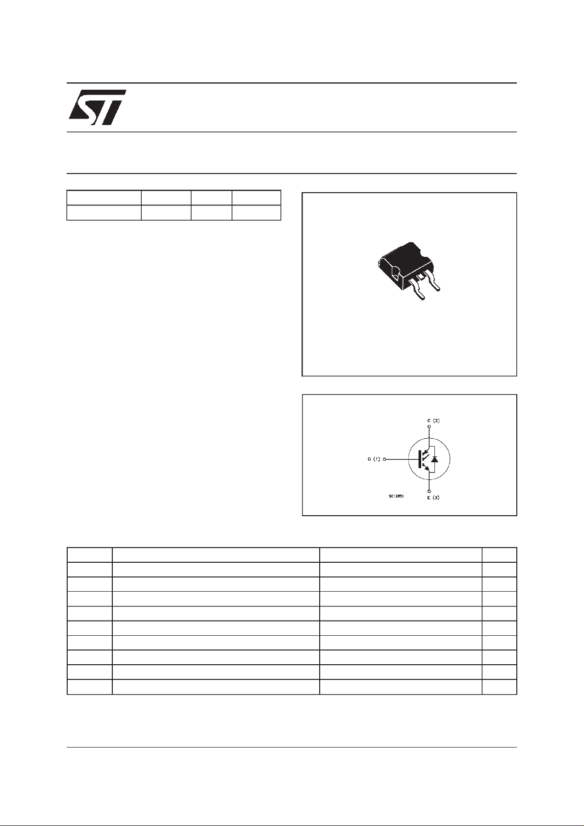
2
PAK(TO-263)
cesat
)
POWERPACKAGE IN TAPE & REEL
(SUFFIX”T4”)
DESCRIPTION
Using the latest high voltage technology based
on a patented strip layout, STMicroelectronics
has designed an advanced family of IGBTs, the
PowerMESH IGBTs, with outstanding
perfomances. The suffix ”H” identifies a family
optimized to achieve very low switching times for
high frequencyapplications(<120kHz).
3
1
D2PAK
TO-263
(Suffix”T4”)
INTERNAL SCHEMATIC DIAGRAM
APPLICATIONS
■ HIGHFREQUENCY MOTOR CONTROLS
■ SMPSAND PFC IN BOTH HARDSWITCH
AND RESONANTTOPOLOGIES
ABSOLUTE MAXIMUM RATINGS
Symb o l Parameter Value Unit
V
V
I
CM
P
T
(•) Pulse width limited by max. junction temperature
June 1999
Collect o r -Em i t t er Volt age (VGS= 0) 600 V
CES
Gate-Emitter V oltage ± 20 V
GE
I
Collect o r Current (continuous ) at Tc=25oC6A
C
I
Collect o r Current (continuous ) at Tc= 100oC3A
C
(•) Collect or Current (pulsed) 24 A
Tot al Dissipation at Tc=25oC70W
tot
Derat ing Fact or 0.56 W/
Sto rage Temperature -65 to 150
stg
T
Max. Oper a t ing Junction Tem perature 150
j
o
C
o
C
o
C
1/8
Page 2
STGB3NB60HD
THERMAL DATA
R
thj-case
R
thj-amb
R
thc-sink
Ther mal Resistanc e Junct ion-case Max
Ther mal Resistanc e Junct ion-ambient Max
Ther mal Resistanc e Case-sink Ty p
1.78
62.5
0.5
o
C/W
o
C/W
o
C/W
ELECTRICAL CHARACTERISTICS
=25oC unless otherwise specified)
(T
j
OFF
Symbol Parameter Test Conditions Min. Typ. M ax. Unit
V
BR(CES)
Collector-Emitter
IC=250µAVGE= 0 600 V
Break dow n Voltage
I
I
CES
GES
Collect o r cut-of f
=0)
(V
GE
Gat e- Em i t t er Leakage
Current (V
CE
=0)
V
=MaxRating Tj=25oC
CE
=MaxRating Tj=125oC
V
CE
V
= ± 20 V VCE=0 ±100 nA
GE
100
1000
ON(∗)
Symbol Parameter Test Conditions Min. Typ. M ax. Unit
V
GE(th)
Gate Th reshold
VCE=VGEIC= 250 µ A35V
Voltage
V
CE(SAT)
Collector-Emitter
Sat urat ion V olt age
VGE=15V IC=3A
V
=15V IC=3A Tj=125oC
GE
2.4
1.9
2.8 V
DYNAMIC
Symbol Parameter Test Conditions Min. Typ. M ax. Unit
C
C
C
Q
Q
g
Q
I
CL
Forward
fs
Tr ansc on duc tance
Input Capaci t ance
ies
Out put Capac it ance
oes
Reverse Transfer
res
Capacit a nc e
Tot al Gate Charge
G
Gate-Emitt er C harge
GE
Gat e- Col lect or C har ge
GC
Latc hing C urrent V
VCE=25 V IC=3A 1.3 2.4 S
VCE=25V f=1MHz VGE= 0 160
23
4.5
VCE= 480 V IC=3A VGE=15V 21
235
33
6.6
300
43
8.6
27 nC
6
7.6
=480V RG=10Ω
clamp
T
= 150oC
j
12 A
µA
µ
V
pF
pF
pF
nC
nC
A
SWITCHINGON
Symbol Param et er Test Co n d i t ions Min. Typ. Max. Uni t
(di/dt)
2/8
t
d(on)
t
r
Eon(❍)
Delay Time
Rise Tim e
Tur n-on Current Slope
on
Tur n-on Switc hing
Losses
VCC= 480 V IC=3A
=15V RG=10Ω
V
GE
V
= 480 V IC=3A
CC
=10Ω VGE=15V
R
G
T
= 125oC
j
16
30
400
77
ns
ns
A/µs
J
µ
Page 3
STGB3NB60HD
ELECTRICAL CHARACTERISTICS
(continued)
SWITCHINGOFF
Symbol Parameter Test Conditions Min. Typ. M ax. Unit
tr(v
t
E
E
tr(v
t
E
E
(off)
d
off
ts
(off)
d
off
ts
t
t
Cross-Over Tim e
c
Off Voltage Rise Time
)
off
Delay Time
t
Fall T ime
f
(**)
Turn-off Switching Loss
(❍)
Tot al Switching Lo ss
Cross-Over Tim e
c
Off Voltage Rise Time
)
off
Delay Time
Fall T ime
t
f
Turn-off Switching Loss
(**)
(❍)
Tot al Switching Lo ss
VCC = 480 V I
R
GE
=10
Ω
VGE=15V
VCC = 480 V I
R
GE
= 125oC
T
j
=10
Ω
VGE=15V
=3A
C
=3A
C
90
36
53
70
33
100
180
82
58
110
88
165
COLLECTOR-EMITTERDIODE
Symbol Param et er Test Co n d itions M i n . Typ. Max. Unit
I
For ward Curre nt
f
I
V
t
Q
I
rrm
(•) Pulse width limited by max. junction temperature
(
❍) Include recovery losses on the STTA306 freewheeling diode
(∗) Pulsed: Pulse duration = 300 µs, duty cycle 1.5%
(**)Losses Include Also The Tail (Jedec Standardization)
For ward Curre nt puls e d
fm
For ward On-Voltage If=3A
f
Reverse Recovery Time
rr
Reverse Recovery Charge
rr
Reverse Recovery Current
=3A Tj= 125oC
I
f
If=3A VR=200 V
dI/dt = 100 A/µST
= 125oC
j
1.6
1.4
87
160
3.7
3
24
2.0 V
ns
ns
ns
ns
µJ
µ
ns
ns
ns
ns
µ
µ
J
J
J
A
A
V
ns
nC
A
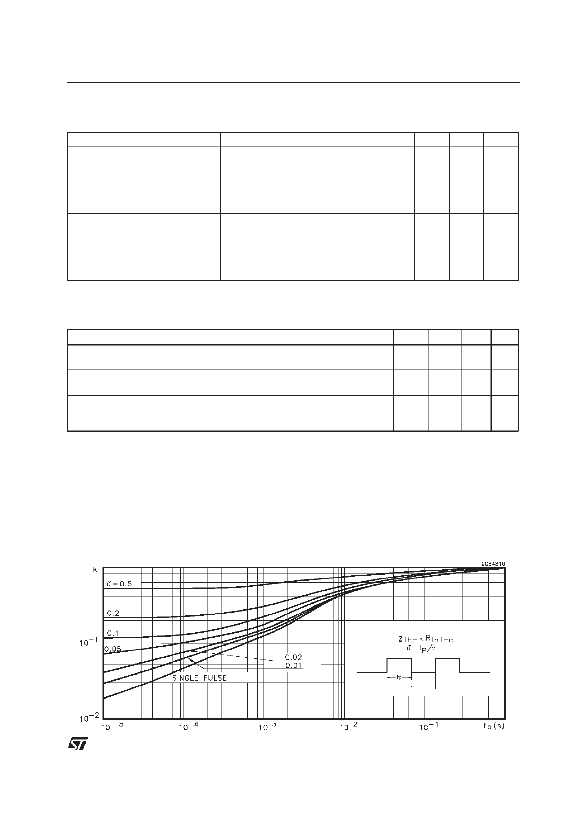
ThermalImpedance
3/8
Page 4

STGB3NB60HD
OutputCharacteristics
Transconductance
TransferCharacteristics
Collector-EmitterOn Voltagevs Temperature
Collector-EmitterOnVoltagevs Collector Current
4/8
Gate Thresholdvs Temperature
Page 5

STGB3NB60HD
NormalizedBreakdown Voltage vs Temperature
Gate Chargevs Gate-EmitterVoltage
CapacitanceVariations
TotalSwitchingLossesvs Gate Resistance
TotalSwitchingLossesvs Temperature
TotalSwitchingLossesvs Collector Current
5/8
Page 6

STGB3NB60HD
SwitchingOff SafeOperatingArea DiodeForwardVoltage
Fig. 1:
Fig. 3
Gate Charge test Circuit
SwitchingWaveforms
Fig. 2:
TestCircuitFor Inductive LoadSwitching
6/8
Page 7

TO-263 (D2PAK) MECHANICAL DATA
STGB3NB60HD
DIM.
MIN. TYP. MAX. MIN. TYP. MAX.
A 4.4 4.6 0.173 0.181
A1 2.49 2.69 0.098 0.106
B 0.7 0.93 0.027 0.036
B2 1.14 1.7 0.044 0.067
C 0.45 0.6 0.017 0.023
C2 1.21 1.36 0.047 0.053
D 8.95 9.35 0.352 0.368
E 10 10.4 0.393 0.409
G 4.88 5.28 0.192 0.208
L 15 15.85 0.590 0.624
L2 1.27 1.4 0.050 0.055
L3 1.4 1.75 0.055 0.068
mm inch
D
A
C2
DETAIL”A”
C
A2
DETAIL”A”
A1
B2
E
L2
L
L3
B
G
P011P6/E
7/8
Page 8

STGB3NB60HD
Information furnished is believedtobeaccurateand reliable.However, STMicroelectronics assumesno responsibility forthe consequences
of use of such information nor for any infringement of patents or other rights of third parties which may resultfrom its use. No license is
granted by implication orotherwise under any patent or patentrights of STMicroelectronics. Specificationmentioned in this publicationare
subjecttochange without notice.Thispublicationsupersedes andreplacesall information previously supplied. STMicroelectronics products
are not authorized for use as critical components in life support devicesor systems without expresswritten approval of STMicroelectronics.
The ST logo is a trademark of STMicroelectronics
1999STMicroelectronics – Printed in Italy – All Rights Reserved
STMicroelectronics GROUP OF COMPANIES
Australia - Brazil - China- Finland - France - Germany - Hong Kong - India - Italy - Japan - Malaysia - Malta - Morocco -
8/8
Singapore - Spain - Sweden - Switzerland - United Kingdom - U.S.A.
http://www.st.com
.
 Loading...