

Datasheet SP6200EM5, SP6200EM5-1-5, SP6200EM5-1-8, SP6200EM5-2-5, SP6200EM5-2-7 Datasheet (Sipex) [ru]
...Page 1

SP6200/6201
Micropower, 100mA and 200mA CMOS LDO Regulators
FEATURES
■ Low Dropout Voltage: 160mV @ 100mA
■ High Output Voltage Accuracy: 2%
■ Ultra Low Shutdown Current: 1µA Max
■ Ultra Low GND Current:
• 200µA @ 200mA Load
• 28µA @ 100µA Load
■ Extremely Tight Load and Line Regulation
■ Current and Thermal Limiting
■ RESET Output (V
■ Logic-Controlled Electronic Enable
■ Unconditionally Stable with 1µF Ceramic
■ Fixed Outputs:
• 1.5V, 1.8V, 2.5V, 2.7V, 2.85V, 3.0V, 3.3V, 3.5V, 5V
■ Adjustable Output Available
■ Tiny DFN Package (2mmX3mm) or SOT23-5
OUT
good)
Now Available in Lead Free Packaging
APPLICATIONS
■ Cellular Telephones
■ Laptop, Notebooks and Palmtop Computers
■ Battery-Powered Equipment
■ Consumer/ Personal Electronics
■ SMPS Post-Regulator
■ DC-to-DC Modules
■ Medical Devices
■ Data Cable
■ Pagers
NC
VIN
VOUT
NC
1
2
3
4
SP6201
8 Pin DFN
8
EN
7
GND
6
NC
5
RESET/ADJ
DESCRIPTION
The SP6200 and SP6201 are CMOS Low Dropout (LDO) regulators designed to meet a broad range of applications that
require accuracy, speed and ease of use. These LDOs offer extremely low quiescent current which only increases
slightly under load, thus providing advantages in ground current performance over bipolar LDOs. The LDOs handle an
extremely wide load range and guarantee stability with a 1µF ceramic output capacitor. They have excellent low
frequency Power Supply Rejection Ratio (PSRR), not found in other CMOS LDOs and thus offer exceptional Line
Regulation. High frequency PSRR is better than 40dB up to 400kHz. Load Regulation is excellent and temperature
stability is comparable to bipolar LDOs. An enable feature is provided on all versions.
The SP6200/6201 is available in fixed and adjustable output voltage versions in tiny DFN and small SOT-23-5
packages. A V
good indicator is provided on all fixed output versions.
OUT
TYPICAL APPLICATION CIRCUIT
Fixed Output Voltage
V
IN
1
5
CIN = 1µF
2
SP6200
Enable
Shutdown
Date: 5/5/06 Rev A SP6200/6201 100/200mA CMOS LDO Regulator © Copyright 2006 Sipex Corporation
EN
EN (pin 3) may be connected
directly to IN (pin 1).
3
SP6201
4
470kΩ
RSN
V
OUT
C
= 1µF
OUT
(V
good)
OUT
1
Page 2

ABSOLUTE MAXIMUM RATINGS, NOTE 1
These are stress ratings only and functional operation of
the device at these ratings or any other above those
indicated in the operation sections of the specifications
below is not implied. Exposure to absolute maximum
rating conditions for extended periods of time may affect
reliability.
Supply Input Voltage (VIN)............................. -2V to 7V
Output Voltage (V
Enable Input Voltage (VEN)............................ -2V to 7V
Power Dissipation (PD).......... Internally Limited, No t e 3
Lead Temperature (soldering 5s)....................... 260°C
Storage Temperature ........................ -65˚C to +150˚C
) ......................... -0.6 to ( VIN +1V)
OUT
OPERATING RATINGS, NOTE 2
Input Voltage (VIN)..................................+2.5V to +6V
Enable Input Voltage (VEN)..........................0V to +6V
Junction Temperature (TJ)................-40˚C to +125˚C
Thermal Resistance (See Note 3):
SOT-23-5 (θ
8 Pin DFN (θ
).................................................191˚C/W
JA
)............................................ .....59˚C/W
JA
(See Note 3)
+1V, VO = 5V for ADJ, IL = 100µA, CIN = 1.0µF, C
OUT
which apply over the full operating temperature range, unless otherwise specified.
PARAMETER MIN TYP MAX UNIT ♦ CONDITIONS
Output Voltage Accuracy, (VO)-22%Variation from specified V
Reference Voltage 1.213 1.250 1.287 V
Output Voltage Temperature 60 ppm/ °C
Coefficient, Note 4, (∆VO/∆T)
Minimum Supply Voltage 2.50 2.70 V IL = 100µA
Line Regulation, (∆VO/ VIN) 0.03 0.2 %/ V
Load Regulation, Note 5, (∆V
) 0.07 0.25 %
O / VO
SP6200-1.5V & 1.8 Load Regulation 0.3 1 % IL = 0.1mA to 100mA, V
SP6201-1.5V & 1.8 Load Regulation 0.3 1 % IL = 0.1mA to 200mA, V
Dropout Voltage, Note 6, (VIN – VO) 0.2 4 mV IL = 100µA
(Not applicable to voltage options below 7 mV
2.7V) 70 120 mV IL = 50mA
Shutdown Quiescent Current, (I
Ground Pin Current, Note 7, (I
) 0.01 1 µA
GND
)2840µAV
GND
Power Supply Rejection Ratio, 78 Frequency =100Hz,
(PSRR) 40 dB Frequency = 400Hz,
Current Limit, (ICL) 100 140 200 mA ♦ SP6200
Thermal Limit 162 °C Turns On
= 1.0µF, TJ = 25°C , unless otherwise specified. The ♦ denotes the specifications
OUT
-3 3 %
♦
♦
Adjustable version only
2.55 2.80 V IL = 50mA
2.70 2.95 V IL = 100mA
3.00 3.50 V IC = 200mA
♦
0.14 0.50 %
VIN = (V
♦
IL = 0.1mA to 100mA, SP6200
♦
IL = 0.1mA to 200mA, SP6201
+ 1V) to 6V
OUT
♦
160 mV
♦
160 250 mV IL = 100mA
300 mV
♦
320 400 mV IL = 200mA, SP6201 Only
500 mV
45 µA
110 200 µAV
250 µA
200 400 µAV
500 µA
♦
♦
V
≥ 0.4V
EN
≥ 2.0V, IL = 100µA
EN
♦
≥2.0V, IL = 100mA, SP6200
EN
♦
only (for 1.5 & 1.8, VIN = 2.95)
≥2.0V, IL = 200mA, SP6201
EN
♦
Only (for 1.5 & 1.8, VIN = 3.5)
300 420 600 mA ♦ SP6201
147 °C Turns Off
IN
IN
IL =10mA
IL =10mA
VIN = V
ELECTRICAL CHARACTERISTICS
OUT
= 2.95V
= 3.5V
Date: 5/5/06 Rev A SP6200/6201 100/200mA CMOS LDO Regulator © Copyright 2006 Sipex Corporation
2
Page 3

+1V, VO = 5V for ADJ, IL = 100µA, CIN = 1.0µF, C
OUT
specifications which apply over the full operating temperature range, unless otherwise specified.
= 1.0µF, TJ = 25°C , unless otherwise specified. The ♦ denotes the
OUT
VIN = V
ELECTRICAL CHARACTERISTICS: Continued
PARAMETER MIN TYP MAX UNITS
♦♦
♦ CONDITIONS
♦♦
Thermal Regulation, 0.05 %/W
Note 8, (∆VO/∆PD)
Output Noise, (e
)I
no
150 µVrms 0.1µF from V
= 50mA, CL = 1µF
L
10Hz to 100kHz
OUT
to Adj.
ENABLE INPUT
Enable Input Logic-Low Voltage, 0.4 V ♦ Regulator Shutdown
(VIL)
Enable Input Logic-High Voltage, 1.6 V ♦ Regulator Enabled
(VIH)
Enable Input Current, (IIL), (IIH) 0.01 1 µA ♦ VIL < 0.4V
0.01 1 µA ♦ VIH > 2.0V
Reset Not Output -2 -4 -6 % Threshold
Note 1. Exceeding the absolute maximum rating may damage the device.
Note 2. The device is not guaranteed to function outside its operating rating.
Note 3. The maximum allowable power dissipation at any TA (ambient temperature) is P
Exceeding the maximum allowable power dissipation will result in excessive die temperature, and the regulator will
D (MAX)
= (TJ
– TA) / θϑA.
(MAX)
go into thermal shutdown. The θJA of the SP6200/6201 (all versions) is 191°C/W for the SOT-23-5 and 59°C/W for
the DFN package on a standard 4 layer board (see “Thermal Considerations” section for further details).
Note 4. Output voltage temperature coefficient is defined as the worst case voltage change divided by the total
temperature range.
Note 5. Load Regulation is measured at constant junction temperature using low duty cycle pulse testing. Parts are
tested for load regulation in the load range; from 0.1mA to 100mA, SP6200; from 0.1mA to 200mA, SP6201. Changes
in output voltage due to heating effects are covered by the thermal regulation specification. Not applicable to output
voltages less than 2.5V.
Note 6. Dropout Voltage is defined as the input to output differential at which the output voltage drops 2% below
its nominal value measured at 1V differential. Not applicable to output voltages less than 2.7V.
Note 7. Ground pin current is the regulator quiescent current. The total current drawn from the supply is the sum
of the load current plus the ground pin current.
Note 8. Thermal regulation is defined as the change in output voltage at a time ”t” after a change in power dissipation
is applied, excluding load or line regulation effects. Specifications are for a 100mA load pulse at VIN = 6V for t = 10ms.
Date: 5/5/06 Rev A SP6200/6201 100/200mA CMOS LDO Regulator © Copyright 2006 Sipex Corporation
3
Page 4
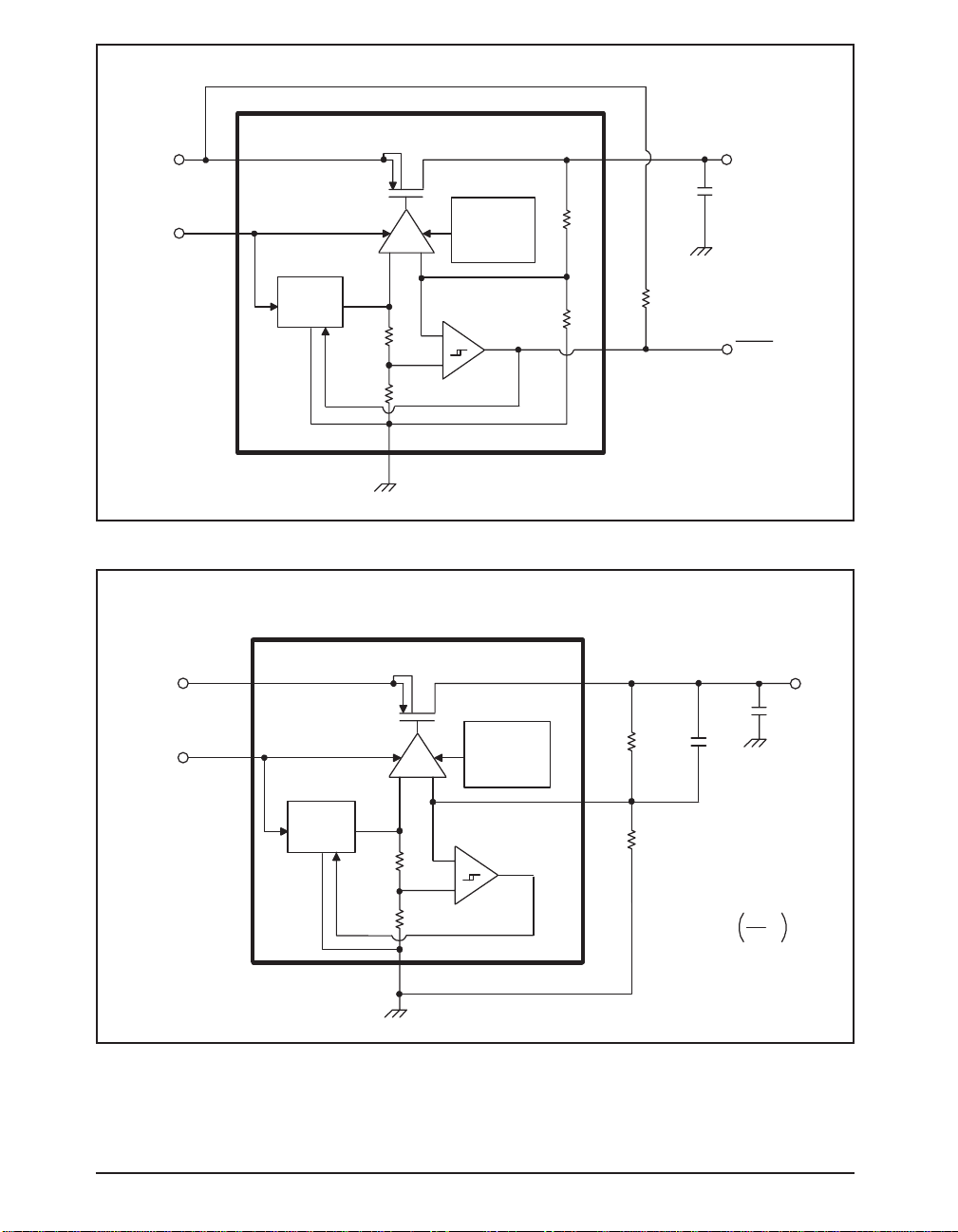
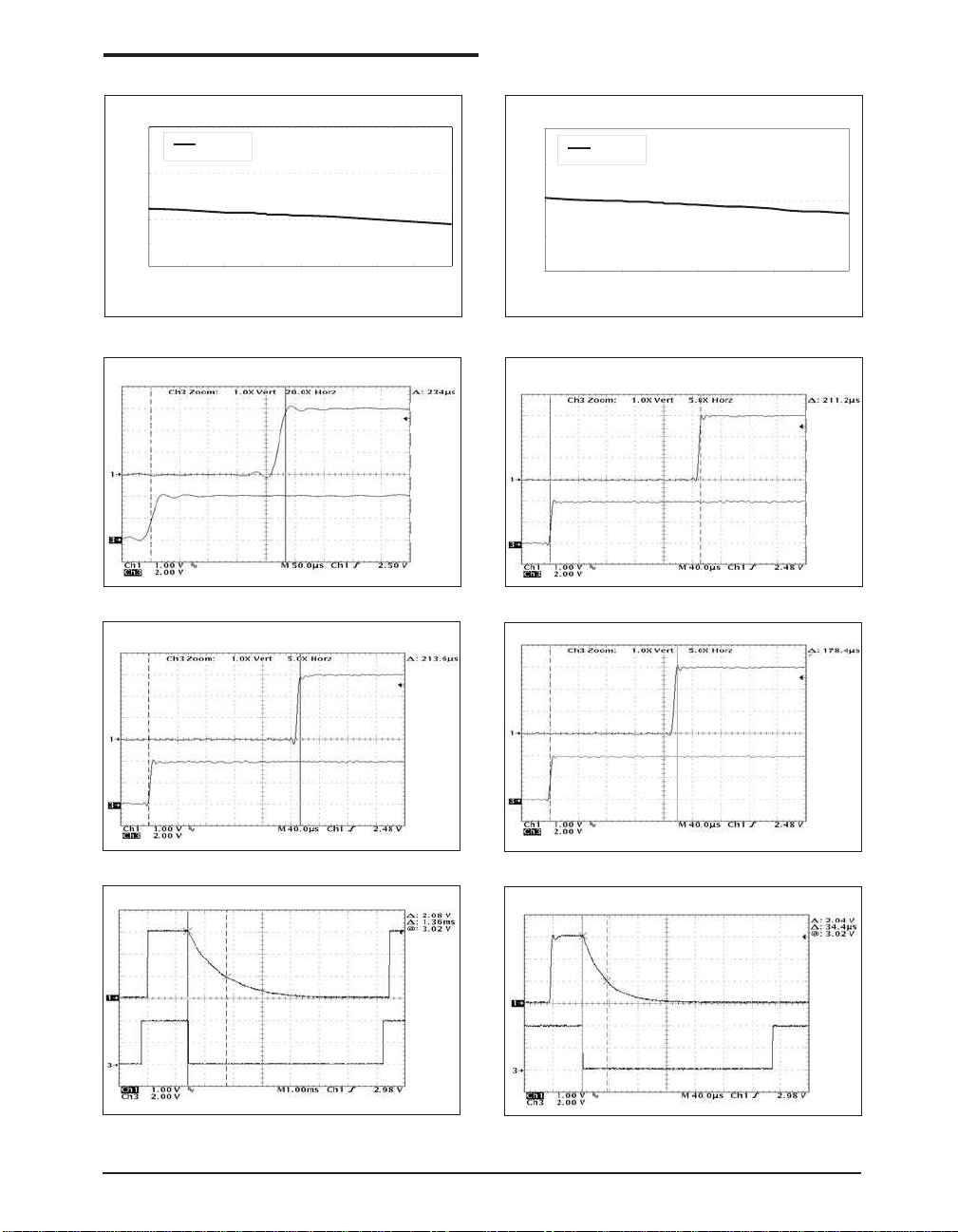
V
IN
Enable
Bandgap
REF
Figure 1. Fixed Voltage Regulator
V
REF
1.25V
GND
-
1.20V
+
Current Limit
and Thermal
Shutdown
R2
R1
OUT
RSN
V
OUT
C
OUT
R
PULL
RESET
V
Enable
IN
IN
EN
Bandgap
REF
V
REF
1.25V
GND
-
1.20V
+
Current Limit
and Thermal
Shutdown
RSN
ADJ
OUT
R2
R1
V
OUT
C
OUT
C
BYP
(option)
= V
REF
R2
R1
+1
V
OUT
Figure 2. Adjustable Voltage Regulator
Date: 5/5/06 Rev A SP6200/6201 100/200mA CMOS LDO Regulator © Copyright 2006 Sipex Corporation
4
Page 5

SOT 23-5 PIN CONFIGURATION
PIN NUMBER NAME FUNCTION
1INSupply Input
2 GND Ground
3ENEnable/Shutdown (Input): CMOS or TTL compatible
input. Logic high = enable, logic low = shutdown
PIN DESCRIPTION
4 RSN (Reset Not) Open drain indicating that V
OUT
is good
4 ADJ Adjustable (Input): Adjustable regulator feedback
input. Connect resistor voltage divider.
5 OUT Regulator Output
8 PIN DFN PIN CONFIGURATION
PIN NUMBER NAME FUNCTION
1NCNo Connect
2 VIN Supply Input
3 VOUT Regulator Input
4NCNo Connect
5 (Fixed) RSN Open drain indicating that V
OUT
is good
5 (Adj.) ADJ Adjustable (Input): Adjustable regulator feedback
input. Connect resistor voltage divider.
6NCNo Connect
7 GND Ground
8ENEnable/Shutdown (Input): CMOS or TTL compatible
input. Logic high = enable, logic low = shutdown
Date: 5/5/06 Rev A SP6200/6201 100/200mA CMOS LDO Regulator © Copyright 2006 Sipex Corporation
5
Page 6

THEORY OF OPERATION
General Overview
The SP6200 and SP6201 are CMOS LDOs
designed to meet a broad range of applications
that require accuracy, speed and ease of use.
These LDOs offer extremely low quiescent current which only increases slightly under load,
thus providing advantages in ground current
performance over bipolar LDOs. The LDOs
handle an extremely wide load range and guarantee stability with a 1µF ceramic output capacitor. They have excellent low frequency
PSRR, not found in other CMOS LDOs and thus
offer exceptional Line Regulation. High frequency PSRR is better than 40dB up to 400kHz.
Load Regulation is excellent and temperature
stability is comparable to bipolar LDOs. Thus,
overall system accuracy is maintained under all
DC and AC conditions. Enable feature is provided on all versions. A Vout good indicator
(RSN pin) is provided in all the fixed output
voltage devices. An adjustable output version is
also available. Current Limit and Thermal protection is provided internally and is well controlled.
Architecture
The SP6200 and SP6201 are only different in
their current limit threshold. The SP6200 has a
current limit of 140mA, while the SP6201 current limit is 420mA. The SP6201 can provide
pulsed load current of 300mA. The LDOs have
a two stage amplifier which handles an extremely wide load range (10µA to 300mA) and
guarantees stability with a 1µF ceramic load
capacitor. The LDO amplifier has excellent gain
and thus touts PSRR performance not found in
other CMOS LDOs. The amplifier guarantees
no overshoot on power up or while enabled
through the EN pin. The amplifier also contains
an active pull down, so that when the load is
removed quickly the output voltage transient is
minimal; thus output deviation due to load transient is small and fairly well matched when
connecting and disconnecting the load.
An accurate 1.250V bandgap reference is
bootstrapped to the output in fixed output versions of 2.7V and higher. This increases both the
low frequency and high frequency PSRR. The
adjustable version also has the bandgap reference bootstrapped to the output, thus the lowest
externally programmable output voltage is 2.7V.
The 2.5V fixed output version has the bandgap
always connected to the Vin pin. Unlike many
LDOs, the bandgap reference is not brought out
for filtering by the user. This tradeoff was maid
to maintain good PSRR at high frequency (PSRR
can be degraded in a system due to switching
noise coupling into this pin). Also, often leakages of the bypass capacitor or other components cause an error on this high impedance
bandgap node. Thus, this tradeoff has been
made with "ease of use" in mind.
Protection
Current limit behavior is very well controlled,
providing less than 10% variation in the current
limit threshold over the entire temperature range
for both SP6200 and SP6201. The SP6200 has a
current limit of 140mA, while the SP6201 has a
current limit of 420mA. Thermal shutdown activates at 162°C and deactivates at 147°C. Thermal shutdown is very repeatable with only a 2 to
3 degree variation from device to device. Thermal shutdown changes by only 1 to 2 degrees
with Vin change from 4V to 7V.
Enable (Shutdown Not) Input
The LDOs are turned off by pulling the EN pin
low and turned on by pulling it high. If it is not
necessary to shut down the LDO, the EN (pin 3)
should be tied to IN (pin 1) to keep the regulator
output on at all time. The enable threshold is
0.9V and does not change more than 100mV
over the entire temperature and Vin voltage
range. The lot to lot variations in Enable Threshold is also within 100mV. Shutdown current is
guaranteed to be <1uA without requiring the
user to pull enable all the way to 0V. Standard
TTL or CMOS levels will transition the device
from totally on to totally off.
Date: 5/5/06 Rev A SP6200/6201 100/200mA CMOS LDO Regulator © Copyright 2006 Sipex Corporation
6
Page 7

Reset Not (VOUT good) Output
An accurate Vout good indicator is provided on
all the fixed output version devices, pin 4 (RSN),
Figure 1. This is an open drain, logic output that
can be used to hold a microprocessor or microcontroller in a RESET condition when it's power
supplied by Vout is 4% out of nominal regulation. A 1% hysteresis is included in the Reset
Not function, so that false alarms are not issued
as a result of LDO's output noise. The Reset Not
function reacts in 10 to 50µs.
Adjustable Output Version
The adjustable version can be programmed to
any voltage from 2.7V to 6V for the industrial
temperature range; 2.5V to 6V for the commercial temperature range. The output can not be
programmed below 2.5V due a headroom restriction. Since the bandgap is bootstrapped to
the output, the output voltage must be above the
minimum bandgap supply voltage. The bandgap
requires 2.7V or greater at -40°C and requires
2.5V or greater at 0°C.
The regulator's output can be adjusted to a
specific output voltage by using two external
resistors, Figure 2. The resistor's set the output
voltage based on the following equation:
V
= 1.25 (R2/R1 + 1)
OUT
Resistor values are not critical because the ADJ
node has a high input impedance, but for best
results use resistors of 470kΩ or less. A capacitor from ADJ to Vout pin provides improved
noise performance as is shown in the following
plot.
Noise Performance 10Hz to 100kHz
Adj, Vin = 4.3V, Vout = 3.3V (Cin = Cout = 1uF)
400
300
200
Output Noise (uVrms)
100
1.0E+02 1.0E+03 1.0E+04 1.0E+05 1.0E+06 1.0E+07
Bypass Cap from Vout to FB (pF)
THEORY OF OPERATION: Continued
Input Capacitor
A small capacitor, 1µF or higher, is required
from V
to GND to create a high frequency
IN
bypass for the LDO amplifier. Any ceramic or
tantalum capacitor may be used at the input.
Capacitor ESR (effective series resistance)
should be smaller than 3Ω.
Output Capacitor
An output capacitor is required between V
OUT
and GND to prevent oscillation. A capacitance
as low as 0.22µF can fulfill stability requirements in most applications. A 1µF capacitor
will ensure unconditional stability from no load
to full load over the entire input voltage, output
voltage and temperature range. Larger capacitor
values improve the regulator's transient response.
The output capacitor value may be increased
without limit. The output capacitor should have
an ESR (effective series resistance) below 5Ω
and a resonant frequency above 1MHz.
No Load Stability
The SP6200/6201 will remain stable and in
regulation with no external load (other than the
internal voltage driver) unlike many other voltage regulators. This is especially important in
CMOS RAM keep-alive applications.
Thermal Considerations
The SP6200 is designed to provide 100mA of
continuous current, while the SP6201 will provide 200mA of continuous current. Maximum
power dissipation can be calculated based on the
output current and the voltage drop across the
part. To determine the maximum power dissipation in the package, use the junction-to-ambient
thermal resistance of the device and the following basic equation:
(T
PD =
T
is the maximum junction temperature of
J(max)
J(max)
θ
- TA)
JA
the die and is 125°C. TA is the ambient operating.
θJA is the junction-to-ambient thermal resistance
for the regulator and is layout dependent.
The actual power dissipation of the regulator
circuit can be determined using one simple
Date: 5/5/06 Rev A SP6200/6201 100/200mA CMOS LDO Regulator © Copyright 2006 Sipex Corporation
7
Page 8

equation:
THEORY OF OPERATION: Continued
= (VIN - V
P
D
Substituting P
≅ (VIN - V
D(max)
)*I
OUT
OUT
) * I
+ VIN*I
OUT
GND
OUT
for PD and solving for the
operating conditions that are critical to the application will give the maximum operating conditions for the regulator circuit. For example, if
we are operating the SP6201- 3.0V at room
temperature, with a SOT-23-5 package on a 4
layer standard board we can determine the maximum input voltage for a set output current.
P
D(max)
(125°C -25°C)
=
(191°C/W)
= 0.52W
To prevent the device from entering thermal
shutdown, maximum power dissipation can not
be exceeded. Using the output voltage of 3.0V
and an output current of 200 mA, the maximum
input voltage can be determined. Ground pin
current can be taken from the electrical spec’stable (I
mum input voltage is determined as follows:
=200uA at I
GND
=200mA). The maxi-
OUT
0.52W = (VIN – 3.0V)*200mA + VIN*0.2mA
Solving for VIN, we get:
(0.52W + 0.6W)
VIN =
200.2mA
After calculations, we find that the maximum
input voltage of a 3.0V application at 200mA of
output current in an SOT-23-5 package is 5.59V.
Dual-Supply Operation
When used in dual supply systems where the
regulator load is returned to a negative supply,
the output voltage must be diode clamped to
ground.
Date: 5/5/06 Rev A SP6200/6201 100/200mA CMOS LDO Regulator © Copyright 2006 Sipex Corporation
8
Page 9

27°C, VIN = 5.5V, IO = 0.1mA, CIN = C
= 1µF unless otherwise specified.
OUT
Dropout vs. Io (SP6201 fixed 3.0V)
400
350
300
250
200
150
Dropout (mV)
100
50
0
050100 150 200
T=125 deg
T=27deg
T=-40 deg
Io (mA)
TYPICAL CHARACTERISTICS
400
350
300
250
200
150
Dropout (mV)
100
50
0
-50 -20 10 40 70 100 130
Dropout vs. Temp (SP6201 fixed 3.0V)
Io=200mA
Io=100mA
Io=50mA
Temp (deg)
Dropout vs. Temp (SP6201 fixed 3.0V)
2.5
2.0
1.5
1.0
Dropout (mV)
0.5
0.0
-50 -20 10 40 70 100 130
Io=1mA
Io=0.1mA
Temp (deg)
Iq vs. Temp (SP6201 fixed 3.0V, EN=Vin, Io=0uA)
50
45
40
Iq (uA)
35
30
25
-50 -20 10 40 70 100 130
350
300
250
200
150
Ignd (uA)
100
50
0
34567
Vin = 7V
Vin =5.5V
Vin = 4V
Temp (deg)
Ignd vs. Vin (SP6201 fixed 3.0V)
Io=200mA
Io=150mA
Io=100mA
Io=50mA
Io=0.1mA
Vin (V)
50
45
40
35
30
25
Iq (uA)
20
15
10
5
0
01234567
250
200
150
100
Iq (nA)
50
0
-50 -20 10 40 70 100 130
220
195
170
145
120
Ignd (uA)
95
70
45
20
050100150 200
Iq vs. Vin (fixed 3.0V, Io=0uA)
EN = Vin
EN = 0V
Vin (V)
Iq vs. Temp (SP6201 fixed 3.0V, EN=0V, Io=0uA)
Vin = 7V
Vin = 5.5V
Vin = 4V
Temp (deg)
Ignd vs. Io (SP6201 fixed 3.0V)
Vin = 7V
Vin = 5.5V
Vin = 4V
Io (mA)
35
30
25
20
Iq (nA)
15
10
5
0
Date: 5/5/06 Rev A SP6200/6201 100/200mA CMOS LDO Regulator © Copyright 2006 Sipex Corporation
9
Page 10

27°C, VIN = 5.5V, IO = 0.1mA, CIN = C
= 1µF unless otherwise specified.
OUT
TYPICAL CHARACTERISTICS: Continued
3.03
3.02
3.01
3.00
Vout (V)
2.99
2.98
2.97
-50 -20 10 40 70 100 130
2.90
2.85
2.80
2.75
Vout (V)
2.70
2.65
-50 -20 10 40 70 100 130
2.525
2.520
2.515
2.510
2.505
2.500
Vout (V)
2.495
2.490
2.485
2.480
2.475
-50 -20 10 40 70 100 130
Vout vs. Temp (fixed 3.0V)
Vin = 7V
Vin = 4V
Vout vs. Temp (adjustable)
2.85Vout
2.7Vout
Vout vs. Temp (adjustable)
2.5Vout
Temp (deg)
Temp (deg)
Temp (deg)
3.33
3.32
3.31
3.30
Vout (V)
3.29
3.28
3.27
-50 -20 10 40 70 100 130
3.35
3.25
3.15
Vout vs. Temp (fixed 3.3V)
Vin = 7V
Vin = 4V
Vout vs. Temp (adjustable)
3.3Vout
3.0Vout
Temp (deg)
Vout (V)
3.05
2.95
-50 -20 10 40 70 100 130
5.05
5.04
5.03
5.02
5.01
5.00
4.99
Vout (V)
4.98
4.97
4.96
4.95
5.0Vout
-50 -20 10 40 70 100 130
Temp (deg)
Vout vs. Temp (adjustable)
Temp (deg)
3.006
3.004
3.002
3.000
Vout (V)
2.998
2.996
2.994
34567
Line Regulation (SP6201 fixed 3.0V)
Io=0.1mA
Io=1mA
Io=50mA
Io=100mA
Io=200mA
Vin (V)
3.004
3.002
3.000
2.998
Vout (V)
2.996
2.994
2.992
050100 150 200 250 300
Load Regulation (SP6201 fixed 3.0V)
Io (mA)
Vin = 7V
Vin = 5.5V
Vin = 4V
Date: 5/5/06 Rev A SP6200/6201 100/200mA CMOS LDO Regulator © Copyright 2006 Sipex Corporation
10
Page 11
27°C, VIN = 5.5V, IO = 0.1mA, CIN = C
= 1µF unless otherwise specified.
OUT
TYPICAL CHARACTERISTICS: Continued
600
Current Limit vs. Temp (fixed 3.3V, Vin=4V)
SP6201-3.3
500
Icl (mA)
400
300
-50 0 50 100 150
Temp (deg)
Turn on time, Io=1mA, 4Vin
V
OUT
SP6201 - 3.0Vout fixed
Ven is toggled, Vin = 4V
Iout = 1mA
Cin = Cout = 1uF Cer. Cap
V
EN
Turn on time, Io=300mA, 4Vin
V
SP6201 - 3.0Vout fixed
Ven is toggled, Vin = 4V
Iout = 300mA
Cin = Cout = 1uF Cer. Cap
OUT
EN
V
200
Current Limit vs. Temp (fixed 3.3V, Vin=4V)
SP6200-3.3
150
Icl (mA)
100
-50 0 50 100 150
Temp (deg)
Turn on time, Io=100mA, 4Vin
3V
2V
1V
0V
4V
2V
0V
SP6201 - 3.0Vout fixed
Ven is toggled, Vin = 4V
Iout = 100mA
Cin = Cout = 1uF Cer. Cap
VOUT
VEN
3V
2V
1V
0V
4V
2V
0V
Turn on time, Io=100mA, 7Vin
V
OUT
3V
2V
1V
0V
4V
2V
0V
SP6201 - 3.0Vout fixed
Ven is toggled, Vin = 7V
Iout = 100mA
Cin = Cout = 1uF Cer. Cap
3V
2V
1V
0V
EN
V
4V
2V
0V
Turn off time, Io=1mA, 4Vin
VOUT
V
EN
SP6201 - 3.0Vout fixed
Ven is toggled, Vin = 4V
Iout= 1mA
Cin = Cout = 1uF Cer. Cap
3V
2V
1V
0V
4V
2V
0V
Turn off time, Io=50mA, 4Vin
V
OUT
V
EN
SP6201 - 3.0Vout fixed
Ven is toggled, Vin = 4V
Iout = 50mA
Cin = Cout = 1uF Cer. Cap
3V
2V
1V
0V
4V
2V
0V
Date: 5/5/06 Rev A SP6200/6201 100/200mA CMOS LDO Regulator © Copyright 2006 Sipex Corporation
11
Page 12

27°C, VIN = 5.5V, IO = 0.1mA, CIN = C
Turn off time, Io=100mA, 4Vin
= 1µF unless otherwise specified.
OUT
TYPICAL CHARACTERISTICS: Continued
Turn off time, Io=100mA, 7Vin
SP6201 - 3.0Vout fixed
V
OUT
Ven is toggled, Vin = 4V
Iout = 100mA
Cin = Cout = 1uF Cer. Cap
V
EN
Inrush Current, Io=100mA
SP6201 - 3.0Vout fixed, Vin=4V
Ven is toggled, Iout=100mA
650mA
Cin = Cout = 1uF Cer. Cap
V
OUT
V
EN
Load Transient Response, 100mA step, 4Vin
SP6201 - 3.0Vout fixed
Vin = 4V, Iout = 100mA
Cin = Cout = 1uF Cer. Cap
100uA
V
OUT
I
OUT
Tr = Tf = 100ns
3V
2V
1V
0V
4V
2V
0V
750mA
500mA
250mA
0mA
2V
0V
4V
2V
0V
80mV
60mV
40mV
20mV
0mV
-20mV
-40mV
100mA
0mA
VOUT
SP6201 - 3.0Vout fixed
Ven is toggled, Vin = 7V
Iout = 100mA
Cin = Cout = 1uF Cer. Cap
VEN
Inrush Current, Io=100uA
SP6201 - 3.0Vout fixed, Vin=4V
650mA
Ven is toggled, Iout = 100uA
Cin = Cout = 1uF Cer. Cap
I
I
V
OUT
V
EN
Load Transient Response, 100mA step, 7Vin
SP6201 - 3.0Vout fixed
Vin = 7V , Iout = 100mA
Cin = Cout = 1uF Cer. Cap
100uA
V
OUT
I
OUT
Tr = Tf = 100ns
3V
2V
1V
0V
4V
2V
0V
500mA
250mA
0mA
2V
0V
4V
2V
0V
80mV
60mV
40mV
20mV
0mV
-20mV
-40mV
100mA
0mA
Load Transient Response, 200mA step, 4Vin
SP6201 - 3.0Vout fixed
Vin = 4V , Iout = 200mA
Cin = Cout = 1uF Cer. Cap
100uA
V
I
OUT
OUT
Tr = Tf = 100ns
200mV
150mV
100mV
50mV
0mV
-50mV
200mA
100mA
0mA
Load Transient Response, 300mA step, 4Vin
SP6201 - 3.0Vout fixed
Vin = 4V, Iout = 300mA
Cin = Cout = 1uF Cer. Cap
100uA
V
OUT
I
OUT
Tr = Tf = 100ns
200mV
150mV
100mV
50mV
0mV
-50mV
200mA
0mA
Date: 5/5/06 Rev A SP6200/6201 100/200mA CMOS LDO Regulator © Copyright 2006 Sipex Corporation
12
Page 13

27°C, VIN = 5.5V, IO = 0.1mA, CIN = C
= 1µF unless otherwise specified.
OUT
TYPICAL CHARACTERISTICS: Continued
REF LEVEL /DIV
0.000dB 10.000dB
-20
-40
(dB)
-60
-80
-100
Power Supply Rejection Ratio
0
I
OUT
C
OUT
V
IN
V
OUT
10 100 1k 10k 100k 1M 10M
START 10.000Hz STOP 10 000 000.000Hz
Frequency (HZ)
Power Supply Rejection Ratio
REF LEVEL /DIV
0.000dB 10.000dB
0
-20
-40
(dB)
-60
= 100µA
= 1µF
= 4V
= 3V
REF LEVEL /DIV
0.000dB 10.000dB
0
-20
-40
(dB)
-60
-80
-100
10 100 1k 10k 100k 1M 10M
START 10.000Hz STOP 10 000 000.000Hz
Frequency (HZ)
I
C
OUT
OUT
= 1mA
= 2.2µF
Power Supply Rejection Ratio
REF LEVEL /DIV
0.000dB 10.000dB
0
-20
-40
(dB)
-60
Power Supply Rejection Ratio
I
I
= 10mA
-80
-100
10 100 1k 10k 100k 1M 10M
START 10.000Hz STOP 10 000 000.000Hz
Frequency (HZ)
OUT
C
OUT
= 2.2µF
-80
-100
10 100 1k 10k 100k 1M 10M
START 10.000Hz STOP 10 000 000.000Hz
Frequency (HZ)
C
OUT
OUT
= 100mA
= 2.2µF
Date: 5/5/06 Rev A SP6200/6201 100/200mA CMOS LDO Regulator © Copyright 2006 Sipex Corporation
13
Page 14

E1/2
E1
Pin1 Designator
to be within this
INDEX AREA
(D/2 x E1/2)
D/2
5
1
e
TOP VIEW
PACKAGE: 5 PIN SOT-23
D
e1
4
E/2
E
A
A1
2
3
(L1)
b
SIDE VIEW
A2
Seating
Plane
FRONT VIEW
Gauge Plane
ø1
R1
R
L2
ø
Seating
L
Plane
ø1
c
5 Pin SOT-23 JEDEC MO-178 Variation AA
SYMBOL
Dimensions in Millimeters:
Controlling Dimension
Dimensions in Inches
Conversion Factor:
1 Inch = 25.40 mm
MIN NOM MAX MIN NOM MAX
A--1.45
A1 0.00 - 0.15
A2 0.90 1.15 1.30
c0.08-0.22
D
E
E1
2.90 BSC 0.115 BSC
2.80 BSC
1.60 BSC
L0.300.45 0.60
L1
L2
R0.10
R1 0.10
0.60 REF
0.25 BSC
--0.004 - -
-
0.25
--0.057
0.000 - 0.006
0.036 0.045 0.051
0.004 - 0.009
0.111 BSC
0.063 BSC
0.012 0.018 0.024
0.024 REF
0.010 BSC
0.004 - 0.010
Ø0º4º8º0º4º8º
ø1 5º 10º 15º 5º 10º 15º
b0.30-0.50
e
e1
1.90 BSC
0.012 - 0.020
0.038 BSC0.95 BSC
0.075 BSC
SIPEX Pkg Signoff Date/Rev: JL Oct3-05 / Rev A
Date: 5/5/06 Rev A SP6200/6201 100/200mA CMOS LDO Regulator © Copyright 2006 Sipex Corporation
14
Page 15

PACKAGE: 8 PIN DFN
Pin1 Designator
to be within this
INDEX AREA
(D/2 x E/2)
D
D/2
E/2
TOP VIEW
D2
D2/2
5678
E2/2
E
E2
b
K
INDEX AREA
(D/2 x E/2)
L
4321
e
BOTTOM VIEW
ø
A
(A3)
Seating Plane
A1
SIDE VIEW
2x3 8 Pin DFN JEDEC MO-229 VARIATION VCED-2
SYMBOL
A
A1
A3
K
ø
SIPEX Pkg Signoff Date/Rev: JL Aug18-05 / RevA
Date: 5/5/06 Rev A SP6200/6201 100/200mA CMOS LDO Regulator © Copyright 2006 Sipex Corporation
Dimensions in Millimeters:
Controlling Dimension
MIN NOM MAX MIN NOM MAX
0.80 0.90 1.00 0.032 0.036 0.039
0.00 0.02 0.05 0.000 0.001 0.002
0.20 REF 0.008 REF
0.20 - - 0.008 - -
b
D
D2
E
E2
e
L
0º - 14º 0º - 14º
0.18 0.25 0.30 0.008 0.010 0.012
1.50 - 1.75 0.059 - 0.069
3.00 BSC 0.118 BSC
1.60 - 1.90 0.063 - 0.075
0.30 0.40 0.50 0.012 0.016 0.020
Dimensions in Inches
Conversion Factor:
1 Inch = 25.40 mm
0.079 BSC2.00 BSC
0.020 BSC0.50 BSC
15
Page 16

ORDERING INFORMATION
g
Part Number Top Mark
SP6200EM5
EADJ
Temperature
e
Ran
Voltage
Option
-40˚C to +125˚C ADJ 5 Pin SOT-23
Package
Type
SP6200EM5/TR EADJ -40˚C to +125˚C ADJ 5 Pin SOT-23
SP6200EM5-1-5 E15 -40˚C to +125˚C 1.5V 5 Pin SOT-23
SP6200EM5-1-5/TR E15 -40˚C to +125˚C 1.5V 5 Pin SOT-23
SP6200EM5-1-8
E18
-40˚C to +125˚C 1.8V 5 Pin SOT-23
SP6200EM5-1-8/TR E18 -40˚C to +125˚C 1.8V 5 Pin SOT-23
SP6200EM5-2-5 E25 -40˚C to +125˚C 2.5V 5 Pin SOT-23
SP6200EM5-2-5/TR E25 -40˚C to +125˚C 2.5V 5 Pin SOT-23
SP6200EM5-2-7
E27
-40˚C to +125˚C 2.7V 5 Pin SOT-23
SP6200EM5-2-7/TR E27 -40˚C to +125˚C 2.5V 5 Pin SOT-23
SP6200EM5-2-85 E285 -40˚C to +125˚C 2.85V 5 Pin SOT-23
SP6200EM5-2-85/TR E285 -40˚C to +125˚C 2.85V 5 Pin SOT-23
SP6200EM5-3-0
E30
-40˚C to +125˚C 3.0V 5 Pin SOT-23
SP6200EM5-3-0/TR E30 -40˚C to +125˚C 3.0V 5 Pin SOT-23
SP6200EM5-3-3 E33 -40˚C to +125˚C 3.3V 5 Pin SOT-23
SP6200EM5-3-3/TR E33 -40˚C to +125˚C 3.3V 5 Pin SOT-23
SP6200EM5-3-5
E35
-40˚C to +125˚C 3.5V 5 Pin SOT-23
SP6200EM5-3-5/TR E35 -40˚C to +125˚C 3.5V 5 Pin SOT-23
SP6200EM5-5-0 E50 -40˚C to +125˚C 5.0V 5 Pin SOT-23
SP6200EM5-5-0/TR E50 -40˚C to +125˚C 5.0V 5 Pin SOT-23
SP6201EM5
FADJ
-40˚C to +125˚C ADJ 5 Pin SOT-23
SP6201EM5/TR FADJ -40˚C to +125˚C ADJ 5 Pin SOT-23
SP6201EM5-1-5 F15 -40˚C to +125˚C 1.5V 5 Pin SOT-23
SP6201EM5-1-5/TR F15 -40˚C to +125˚C 1.5V 5 Pin SOT-23
SP6201EM5-1-8
F18
-40˚C to +125˚C 1.8V 5 Pin SOT-23
SP6201EM5-1-8/TR F18 -40˚C to +125˚C 1.8V 5 Pin SOT-23
SP6201EM5-2-5 F25 -40˚C to +125˚C 2.5V 5 Pin SOT-23
SP6201EM5-2-5/TR F25 -40˚C to +125˚C 2.5V 5 Pin SOT-23
SP6201EM5-2-7
F27
-40˚C to +125˚C 2.7V 5 Pin SOT-23
SP6201EM5-2-7/TR F27 -40˚C to +125˚C 2.5V 5 Pin SOT-23
SP6201EM5-2-85 F285 -40˚C to +125˚C 2.85V 5 Pin SOT-23
SP6201EM5-2-85/TR F285 -40˚C to +125˚C 2.85V 5 Pin SOT-23
SP6201EM5-3-0
F30
-40˚C to +125˚C 3.0V 5 Pin SOT-23
SP6201EM5-3-0/TR F30 -40˚C to +125˚C 3.0V 5 Pin SOT-23
SP6201EM5-3-3 F33 -40˚C to +125˚C 3.3V 5 Pin SOT-23
SP6201EM5-3-3/TR F33 -40˚C to +125˚C 3.3V 5 Pin SOT-23
SP6201EM5-3-5
F35
-40˚C to +125˚C 3.5V 5 Pin SOT-23
SP6201EM5-3-5/TR F35 -40˚C to +125˚C 3.5V 5 Pin SOT-23
SP6201EM5-5-0 F50 -40˚C to +125˚C 5.0V 5 Pin SOT-23
SP6201EM5-5-0/TR F50 -40˚C to +125˚C 5.0V 5 Pin SOT-23
Available in lead free packaging. To order add "-L" suffix to part number.
Example: SP6200EM5-1-5/TR = standard; SP6200EM5-L-1-5/TR = lead free. Lead
Free SOT-23 packages can be identified by a Bar “|” to the left of the standard Top Marking.
/TR = Tape and Reel. Pack quantity is 2500 for SOT-23.
Sipex Corporation
Headquarters and
Sales Office
233 South Hillview Drive
Milpitas, CA 95035
Solved By SipexTM
Sipex Corporation reserves the right to make changes to any products described herein. Sipex does not assume any liability arising out of the
application or use of any product or circuit described herein; neither does it convey any license under its patent rights nor the rights of others.
Date: 5/5/06 Rev A SP6200/6201 100/200mA CMOS LDO Regulator © Copyright 2006 Sipex Corporation
TEL: (408) 934-7500
FAX: (408) 935-7600
16
Page 17

ORDERING INFORMATION
g
Part Number Top Mark
SP6200ER
620-0ER
Temperature
Ran
-40˚C to +125˚C ADJ 8 Pin DFN
e
Voltage
Option
Package
Type
SP6200ER/TR 620-0ER -40˚C to +125˚C ADJ 8 Pin DFN
SP6200ER-1-5 620-015 -40˚C to +125˚C 1.5V 8 Pin DFN
SP6200ER-1-5/TR 620-015 -40˚C to +125˚C 1.5V 8 Pin DFN
SP6200ER-1-8
620-018
-40˚C to +125˚C 1.8V 8 Pin DFN
SP6200ER-1-8/TR 620-018 -40˚C to +125˚C 1.8V 8 Pin DFN
SP6200ER-2-5 620-025 -40˚C to +125˚C 2.5V 8 Pin DFN
SP6200ER-2-5/TR 620-025 -40˚C to +125˚C 2.5V 8 Pin DFN
SP6200ER-2-7
620-027
-40˚C to +125˚C 2.7V 8 Pin DFN
SP6200ER-2-7/TR 620-027 -40˚C to +125˚C 2.5V 8 Pin DFN
SP6200ER-2-85 620-0285 -40˚C to +125˚C 2.85V 8 Pin DFN
SP6200ER-2-85/TR 620-0285 -40˚C to +125˚C 2.85V 8 Pin DFN
SP6200ER-3-0
620-030
-40˚C to +125˚C 3.0V 8 Pin DFN
SP6200ER-3-0/TR 620-030 -40˚C to +125˚C 3.0V 8 Pin DFN
SP6200ER-3-3 620-033 -40˚C to +125˚C 3.3V 8 Pin DFN
SP6200ER-3-3/TR 620-033 -40˚C to +125˚C 3.3V 8 Pin DFN
SP6200ER-3-5
620-035
-40˚C to +125˚C 3.5V 8 Pin DFN
SP6200ER-3-5/TR 620-035 -40˚C to +125˚C 3.5V 8 Pin DFN
SP6200ER-5-0 620-050 -40˚C to +125˚C 5.0V 8 Pin DFN
SP6200ER-5-0/TR 620-050 -40˚C to +125˚C 5.0V 8 Pin DFN
SP6201ER
620-1ER
-40˚C to +125˚C ADJ 8 Pin DFN
SP6201ER/TR 620-1ER -40˚C to +125˚C ADJ 8 Pin DFN
SP6201ER-1-5 620-115 -40˚C to +125˚C 1.5V 8 Pin DFN
SP6201ER-1-5/TR 620-115 -40˚C to +125˚C 1.5V 8 Pin DFN
SP6201ER-1-8
620-118
-40˚C to +125˚C 1.8V 8 Pin DFN
SP6201ER-1-8/TR 620-118 -40˚C to +125˚C 1.8V 8 Pin DFN
SP6201ER-2-5 620-125 -40˚C to +125˚C 2.5V 8 Pin DFN
SP6201ER-2-5/TR 620-125 -40˚C to +125˚C 2.5V 8 Pin DFN
SP6201ER-2-7
620-127
-40˚C to +125˚C 2.7V 8 Pin DFN
SP6201ER-2-7/TR 620-127 -40˚C to +125˚C 2.5V 8 Pin DFN
SP6201ER-2-85 620-1285 -40˚C to +125˚C 2.85V 8 Pin DFN
SP6201ER-2-85/TR 620-1285 -40˚C to +125˚C 2.85V 8 Pin DFN
SP6201ER-3-0
620-130
-40˚C to +125˚C 3.0V 8 Pin DFN
SP6201ER-3-0/TR 620-130 -40˚C to +125˚C 3.0V 8 Pin DFN
SP6201ER-3-3 620-133 -40˚C to +125˚C 3.3V 8 Pin DFN
SP6201ER-3-3/TR 620-133 -40˚C to +125˚C 3.3V 8 Pin DFN
SP6201ER-3-5
620-135
-40˚C to +125˚C 3.5V 8 Pin DFN
SP6201ER-3-5/TR 620-135 -40˚C to +125˚C 3.5V 8 Pin DFN
SP6201ER-5-0 620-150 -40˚C to +125˚C 5.0V 8 Pin DFN
SP6201ER-5-0/TR 620-150 -40˚C to +125˚C 5.0V 8 Pin DFN
Available in lead free packaging. To order add "-L" suffix to part number.
Example: SP6200ER-1-5/TR = standard; SP6200ER-L-1-5/TR = lead free.
Lead Free DFN packages can be identified by a Bar “__” under the standard Top Marking.
/TR = Tape and Reel. Pack quantity is 3,000 for DFN.
Sipex Corporation
Headquarters and
Sales Office
233 South Hillview Drive
Milpitas, CA 95035
Solved By SipexTM
Sipex Corporation reserves the right to make changes to any products described herein. Sipex does not assume any liability arising out of the
application or use of any product or circuit described herein; neither does it convey any license under its patent rights nor the rights of others.
Date: 5/5/06 Rev A SP6200/6201 100/200mA CMOS LDO Regulator © Copyright 2006 Sipex Corporation
TEL: (408) 934-7500
FAX: (408) 935-7600
17
Page 18

 Loading...