

Page 1
®
SP6648
Ultra-low Quiescent Current,
High Efficiency Boost Regulator
FEATURES
■ Ultra-low 12µA Quiescent Current
■ 400mA Output Current at 2.6V Input: 3.3V
■ 94% Efficiency from 2 cell to 3.3V
OUT
OUT
■ Wide Input Voltage Range: 0.95V to 4.5V
■ 3.3V Fixed or Adjustable Output
■ Integrated Synchronous Rectifier: 0.3Ω
■ 0.3Ω Switch
■ Anti-Ringing Switch Technology
Now Available in Lead Free Packaging
■ Programmable Inductor Peak Current
■ Logic Shutdown Control
■ Under Voltage Lock-Out at 0.61V
■ Programmable Low Battery Detect
■ Single or Dual Cell Alkaline
■ Small 10 pin DFN Package and Industry
Standard 10 pin MSOP
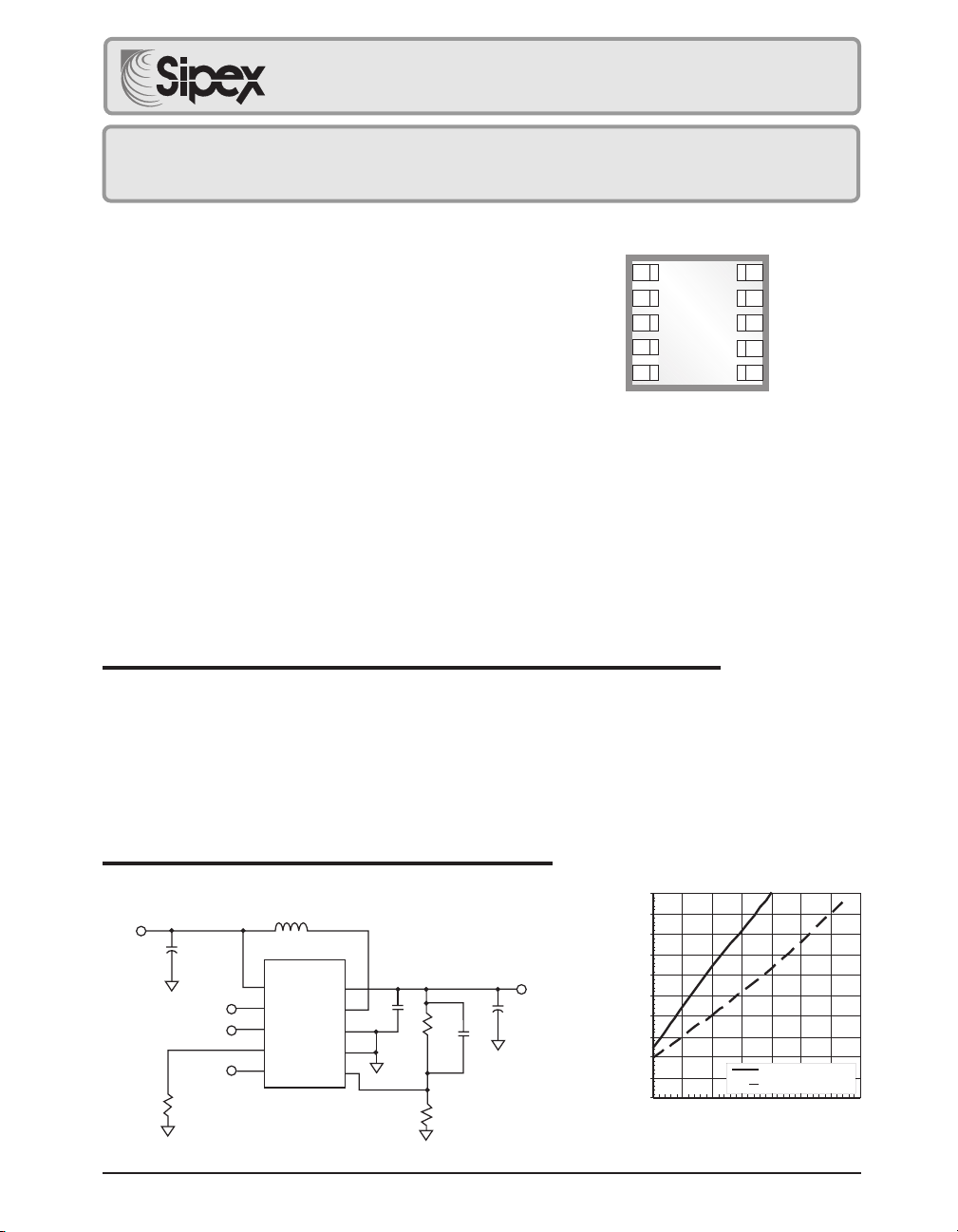
The SP6648 is an ultra-low quiescent current, high efficiency step-up DC-DC converter ideal for
single cell, dual cell alkaline and Li-Ion battery applications such as digital still cameras, PDA’s,
MP3 players, and other portable devices. The SP6648 combines the high delivery associated
with PWM control, and the low quiescent current and excellent light-load efficiency of PFM control.
The SP6648 features 12µA quiescent current, synchronous rectification, a 0.3Ω charging switch,
anti-ringing inductor switch, programmable low battery detect, under-voltage lockout and
programmable inductor peak current. The device can be controlled by a 1nA active LOW
shutdown pin.
V
BATT
LBON
R
SHDN
LBI
LIM
1
2
3
4
5
SP6648
10 Pin DFN
10
V
OUT
9
LX
8
P
GND
7
GND
6
FB
APPLICATIONS
■ Camera Flash LED Driver
■ Wireless Mouse
■ PDA's
■ Pagers
■ Medical Monitors
■ Handheld Portable Devices
■ MP3 Players
DESCRIPTION
TYPICAL APPLICATION CIRCUIT
10µH
V
BATT
+
47µF
1.87K
LBI
LBON
SHDN
1
2
3
4
5
SP6648
V
BATT
LBI
LBON
R
LIM
SHDN
V
P
GND
OUT
GND
10
9
LX
FB
1µF
8
7
6
205K
124K
47pF
3.3V
OUT
+
47µF
500
450
400
350
300
250
Io (mA)
200
150
100
50
0
1.0 1.5 2.0 2.5 3.0 3.5 4.0 4.5
Vout=3.3V, Ipk=0.85A
Vout=5.0V, Ipk=0.85A
Vin (V)
Maximum Load Current in Operation
Date: 1/19/05 SP6648 Ultra-low Quiescent Current, High Efficiency Boost Regulator © Copyright 2005 Sipex Corporation
1
Page 2
ABSOLUTE MAXIMUM RATINGS
LX, Vo, V
SHDN, LBI ........................................................... -0.3V to V
Vo, GND, LX Current ....................................................................... 2A
Reverse V
Forward V
Storage Temperature .................................................. -65 °C to 150°C
, LBON, FB to GND pin ................................ -0.3 to 6.0V
BATT
Current .............................................................. 220mA
BATT
Current .............................................................. 500mA
BATT
BATT
+1.0V
Operating Temperature ................................................ -40°C to +85°C
ESD Rating ........................................................................ 1.5kV HBM
These are stress ratings only and functional operation of the device at
these ratings or any other above those indicated in the operation sections
of the specifications below is not implied. Exposure to absolute maximum
rating conditions for extended periods of time may affect reliability.
ELECTRICAL SPECIFICATIONS
V
BATT =VSHDN
otherwise noted. The
otherwise specified.
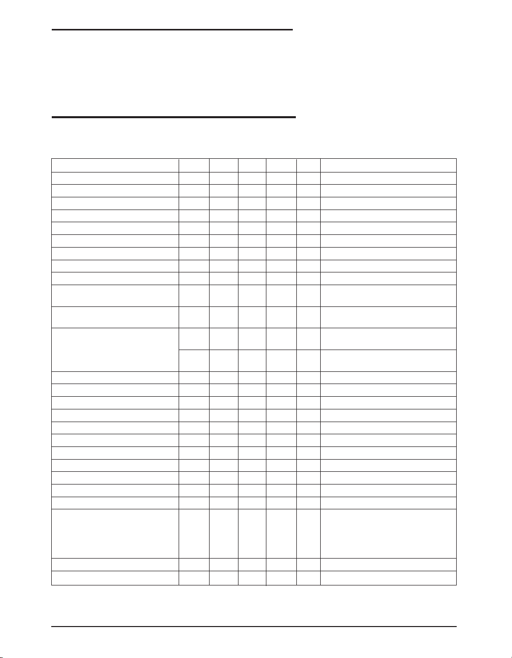
PARAMETER MIN TYP MAX UNITS ♦ CONDITIONS
Input Voltage Operating Range, V
Output Voltage Range, V
Start-up Input Voltage, V
Under Voltage Lock-out/UVLO 0.5 0.61 0.7 V ♦
Output Voltage, V
Quiescent Current into VO, I
Quiescent Current into V
Shutdown Current into V
Shutdown Current into V
Efficiency 84 % V
Inductor Current Limit, IPK = 1600/R
Output Current 200 mA V
Minimum Off-Time Constant K
Maximum On-Time Constant K
Enable Valid to Output Stable 300 500 µsI
NMOS Switch Resistance 0.30 0.6 Ω♦I
PMOS Switch Resistance 0.30 0.6 Ω♦I
FB Set Voltage, V
FB Input Current 1 100 nA ♦ VFB =1.3V
LBI Falling Trip Voltage 0.56 0.61 0.66 V ♦
LBI Hysteresis 25 mV
Low Output Voltage for LBON, V
Leakage current for LBON 1 µA ♦ V
SHDN Input Voltage, Note 1
SHDN Input Current 1 100 nA ♦
LX Pin Leakage 3 µA
Note 1: SHDN must transition faster than 1V/100mS for proper operation.
= 2.6V, VFB=0V, I
LOAD
= 0mA, T
= -40°C to +85°C, V
AMB
= +3.3V, typical values at 27°C unless
OUT
♦ denotes the specifications which apply over full operating temperature range -40°C to +85°C, unless
0.7 4.5 V ♦ After Startup
BATT
OUT
BATT
O
QO
, I
BATT
QB
O, ISDO
BATT, ISDB
OFF
ON
FB
V
IL
V
IH
V
IL
V
IH
2.5 5.5 V ♦
0.85 1.1 V ♦ R
LOAD
= 3kΩ
3.12 3.30 3.48 V ♦ Internal Feedback Divider
12 25 µA ♦ V
250 750 nA ♦ V
1 500 nA ♦ V
250 750 nA ♦ V
92 % V
650 800 1000 mA ♦ R
LIM
1300 1600 2000 mA ♦ R
100 mA V
150 mA V
400 mA V
0.5 1.0 1.5 V*µs ♦ K
2.5 4.0 5.5 V*µs ♦ KON ≥ T
OUT
OUT
SHDN
SHDN
BATT
BATT
LIM
LIM
BATT
BATT
BATT
BATT
OFF
LOAD
NMOS
PMOS
= 3.3V, V
= 3.3V, V
= 0V
= 0V, V
= 1.3V, I
= 2.6V, I
= 2kΩ
= 1kΩ
= 1.3V, R
= 2.6V, R
= 1.3V, R
= 2.6V, R
≤ T
OFF (VOUT
ON (VBATT
= 1mA
= 100mA
= 100mA
1.19 1.25 1.31 V ♦ External feedback
OL
0.4 V ♦ V
0.25 ♦ V
1.0 V ♦ V
0.5 ♦ V
2.0 ♦ V
= 1.3V, I
BATT
= 1.3V, V
BATT
= 1.3V
BATT
= 1.3V
BATT
= 2.6V
BATT
= 2.6V
BATT
= 1.5V, Toggle SHDN
FB
= 1.5V
FB
= 2.6V
BATT
= 100mA, R
OUT
= 200mA, R
OUT
= 4kΩ
LIM
= 4kΩ
LIM
=2kΩ
LIM
=2kΩ
LIM
- V
BATT
LIM =
LIM =
)
)
= 1mA
SINK
= 3.3V
LBON
2kΩ
2kΩ
Date: 1/19/05 SP6648 Ultra-low Quiescent Current, High Efficiency Boost Regulator © Copyright 2005 Sipex Corporation
2
Page 3
PIN DESCRIPTION
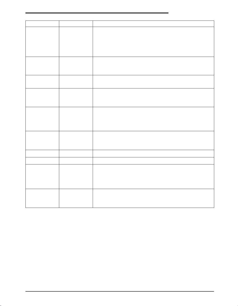
PIN NUMBER PIN NAME DESCRIPTION
1V
BATT
2 LBI Low Battery Input. LBI below 0.61V causes the SP6648 pin to pull
3 LBON Low Battery Output Not. Open drain NMOS output that sinks current
4R
LIM
5 SHDN Shutdown Not. Tie this pin high to V
6FBFeedback. Connect this pin to GND for fixed +3.3V operation.
7 GND Ground. Connect to ground plane.
8 PGND Power Ground. The inductor charging current flows out of this pin.
9LXInductor Switching Node. Connect one terminal of the inductor to the
10 V
OUT
Battery Voltage. The startup circuitry is powered by this pin. Battery
Voltage is used to calculate switch off time: t
V
). When the battery voltage drops below 0.61V the SP6648
BATT
OFF
= K
OFF
goes into an undervoltage lockout mode (UVLO), where the part is shut
down.
LBON pin down to ground. Use a resistor divider to program the low
voltage threshold for a specific battery configuration.
to ground when LBI is below 0.61V.
Current Limit Resistor. By connecting a resistor R
ground the inductor peak current is set by I
for R
is 9kΩ (for 180mA) to 1.KΩ (for 1.6A).
LIM
PEAK
for normal operation. Pull
BATT,
from this pin to
LIM
=1600/R
this pin to ground to disable all circuitry inside the chip. In shutdown
the output voltage will float down to a diode drop below the battery
voltage.
Connect this pin to a resistor voltage divider between V
for adjustable output operation.
positive terminal of the battery. Connect the second terminal of the
inductor to this pin. The inductor charging current flows into LX,
through the internal charging N-channel FET, and out the PGND pin.
Output Voltage. The inductor current flows out of this pin during
switch off-time. It is also used as the internal regulator voltage supply.
Connect this pin to the positive terminal of the output capacitor.
/ (V
OUT
. The range
LIM
and GND
OUT
-
Date: 1/19/05 SP6648 Ultra-low Quiescent Current, High Efficiency Boost Regulator © Copyright 2005 Sipex Corporation
3
Page 4
FUNCTIONAL DIAGRAM
SHDN
FB
R
LIM
LBI
V
BATT
charge end
switch
buffer
IUC
QKILL
V
O
1.25V
+
c
-
current
reference
V
BATT
T
Min
OFF
T
OFF
-
UVLO
c
+
REF
+
VOLOW
c
FB
-
VO
QR
CHARGE
SQn
SP6648
INTERNAL
V
BATT
SDI
0.61V
O
V
n
Ref
Block
current
control
-
+
IBIAS
0.61V
c
SDI
Ipkset
0.61V
NMOS
QKILL
PMOS
LX
LX
current
reference
+
V
BATT
undercurrent
comparator
c
-
INTERNAL
SUPPLY
V
O
Max
Ton
+
c
-
overcurrent
comparator
SWITCH GROUND
INTERNAL
GROUND
P
V
GND
GND
OUT
LOAD
LBON
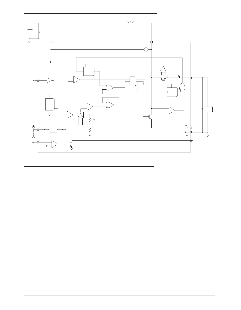
THEORY OF OPERATION
Detailed Description
The SP6648 is a step-up DC-DC converter that
can start up with input voltages as low as 0.85V
(typically) and operates with an input voltage
down to 0.61V. Ultra low quiescent current of
12µA provides excellent efficiency, up to 94%.
In addition to the main switch, a 0.3Ω internal
MOSFET the SP6648 has an internal synchronous rectifier, increasing efficiency and reducing the space of an external diode. An internal
inductive-damping switch significantly reduces
inductive ringing for low noise high efficiency
Control Scheme
A minimum off-time, current limited pulse frequency modulation (PFM) control scheme combines the high output power and efficiency of a
pulse width modulation (PWM) device with the
ultra low quiescent current of the traditional
PFM. At low to moderate output loads the PFM
control provides higher efficiency than traditional PWM converters are capable of delivering. At these loads the switching frequency is
determined by a minimum off-time (t
and a maximum on-time (tON,
MAX
OFF, MIN
) where:
operation. If the supply voltage drops below
0.61V the SP6648 goes into under voltage lockout, thus opening both internal switches. An
externally programmable low battery detector
with open drain output provides the ability to
flag battery low condition. The inductor peak
current is externally programmable to allow for
t
OFF
≥ K
OFF
/ (V
tON ≤ KON / V
K
= 1.0Vµs and
OFF
KON = 4.0Vµs.
OUT
BATT
- V
with
BATT
) and
a range of inductor values.
Date: 1/19/05 SP6648 Ultra-low Quiescent Current, High Efficiency Boost Regulator © Copyright 2005 Sipex Corporation
4
)
Page 5
THEORY OF OPERATION: Continued
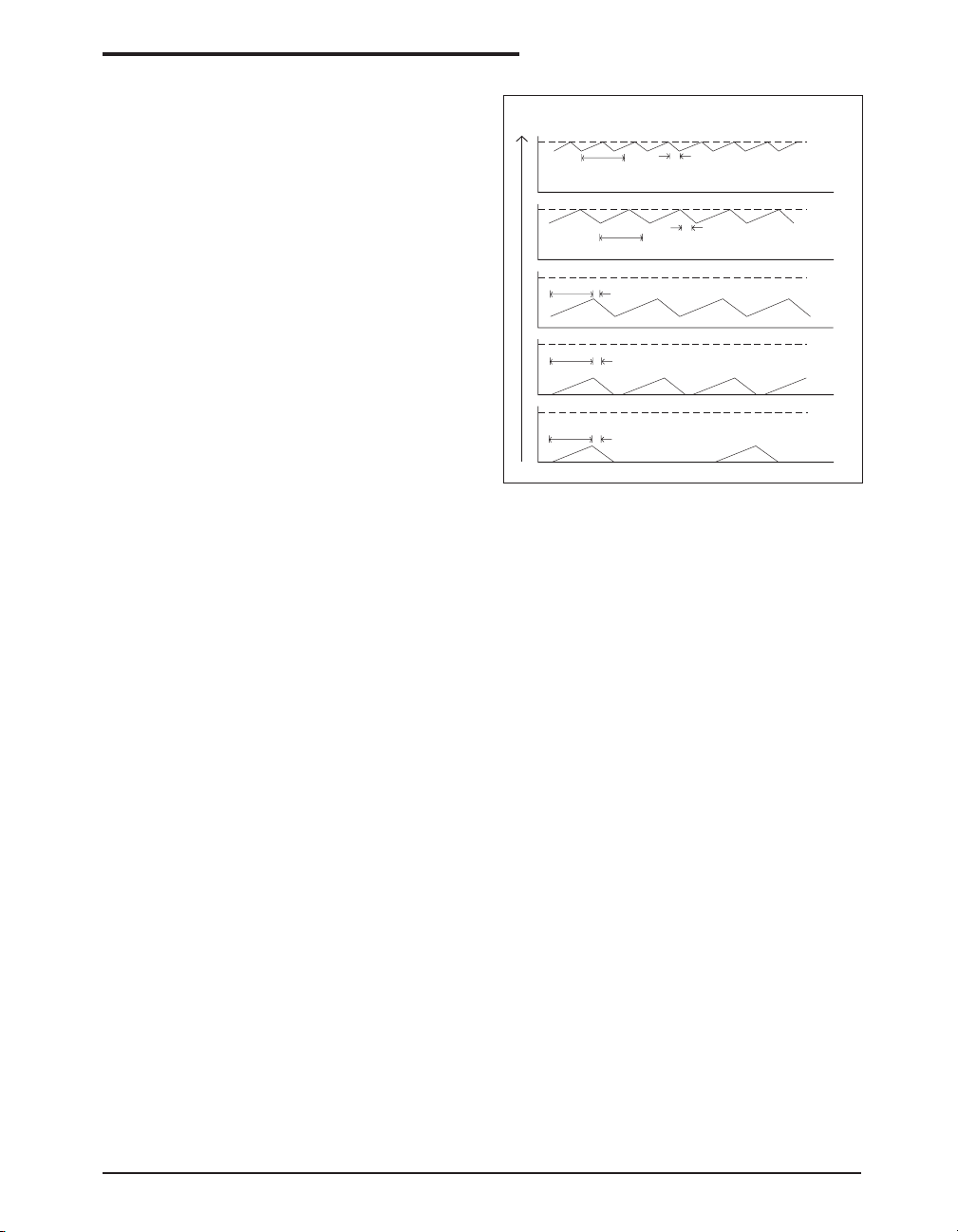
At light loads (as shown in plot A in Figure 1)
the charge cycle will last the maximum value for
tON: For a 1V battery this would be as follows:
t
= KON / V
ON
= 4.0Vµs / 1V = 4.0µs
BATT
The current built up in the coil during the charge
cycle gets fully discharged (discontinuous conduction mode DCM) When the current in the
coil has reached zero the synchronous rectifier
switch is opened and the voltage across the coil
(from V
to LX) is shorted internally to
BATT
eliminate inductive ringing.
With increasing load (as shown in plot B in
Figure 1) this inductor damping time becomes
shorter, because the output will quickly drop
below its regulation point due to heavier load. If
the load current increases further the SP6648
enters continuous conduction mode (CCM)
where there is always current flowing in the
inductor. The charge time remains at maximum
tON as long as the inductor peak current limit is
not reached as shown in plot C in Figure 1. The
inductor peak current limit can be programmed
by tying a resistor R
from the R
LIM
LIM
pin to
ground where:
I
= 1600 / R
PEAK
LIM
Inductor Current vs. Load
Ton Max. Toff Min.
Ton Max.
Ton Max.
Toff Min.
Ton Max.
Toff Min.
Ton Max.
Toff Min.
E. Iripple=Toff* (Vo
Toff Min.
- Vi)/L<Iripple<Ton*Vi/L
D. Toff*= (Vo
C. Iripple=Ton*Vi/L
B. Iripple=Ton*Vi/L
A. Iripple=Ton*Vi/L
- Vi)/L
llim
E
llim
D
llim
C
llim
B
llim
A
Figure 1. Inductor Current vs. Load
which ends the charge cycle and starts the discharge cycle. However, full load is not yet
achieved because at the end of the minimum
discharge time the output was still within regulation.
Maximum load is reached when this discharge
time has shrunk to the minimum allowed value
T
as shown in Plot E of Figure 1.
OFF
When the peak current limit is reached the
charge time is short-cycled.
In plot D of Figure 1, the switch current reaches
the peak current limit during the charge period
Date: 1/19/05 SP6648 Ultra-low Quiescent Current, High Efficiency Boost Regulator © Copyright 2005 Sipex Corporation
5
Page 6
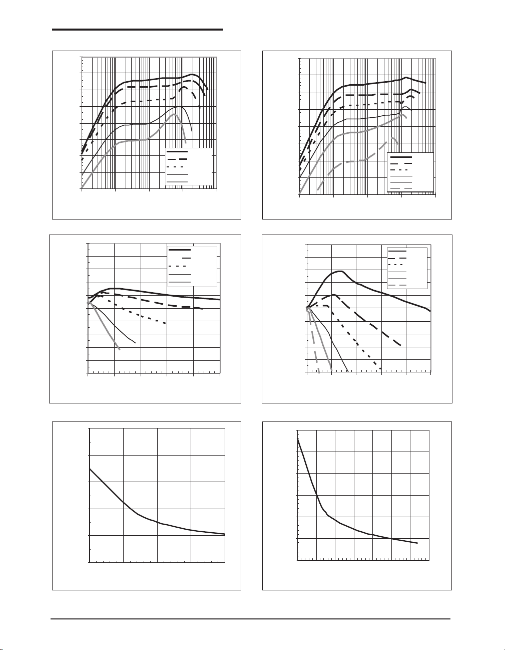
TYPICAL PERFORMANCE CHARACTERISTICS
Refer to the Typical Application Circuit on page 1, T
100
95
90
85
80
75
Efficiency (%)
70
65
60
0.1 1.0 10.0 100.0 1000.0
Iload (mA)
Efficiency vs. Load Current, V
OUT
3.400
3.380
3.360
3.340
3.320
(V)
3.300
OUT
V
3.280
3.260
3.240
3.220
3.200
0 100 200 300 400 500
I
(mA)
LOAD
Line/Load Rejection vs. Load Current, V
=3.3V
Vi=3.0V
Vi=2.6V
Vi=2.0V
Vi=1.3V
Vi=1.0V
Vi=3.0V
Vi=2.6V
Vi=2.0V
Vi=1.3V
Vi=1.0V
OUT
= 3.3V
=+25°C.
AMB
100
95
90
85
80
Efficiency (%)
75
70
65
60
0.1 1.0 10.0 100.0 1000.0
Efficiency vs. Current Load, V
5.100
5.080
5.060
5.040
5.020
5.000
Vout (V)
4.980
4.960
4.940
4.920
4.900
0 100 200 300 400 500
Iload (mA)
=5.0V
OUT
Iload (mA)
Line/Load Rejection vs. Load Current, V
OUT
Vi=4.2V
Vi=3.2V
Vi=2.6V
Vi=2.0V
Vi=1.6V
Vi=1.0V
Vi=4.2V
Vi=3.2V
Vi=2.6V
Vi=2.0V
Vi=1.6V
Vi=1.0V
= 5.0V
100
80
60
Iin (uA)
40
20
0
1.0 1.5 2.0 2.5 3.0
No Load Battery Current, V
Date: 1/19/05 SP6648 Ultra-low Quiescent Current, High Efficiency Boost Regulator © Copyright 2005 Sipex Corporation
OUT
Vin (V)
=3.3V
300
250
200
150
Iin (uA)
100
50
0
1.0 1.5 2.0 2.5 3.0 3.5 4.0 4.5
No Load Battery Current, V
Vin (V)
OUT
=5.0V
6
Page 7
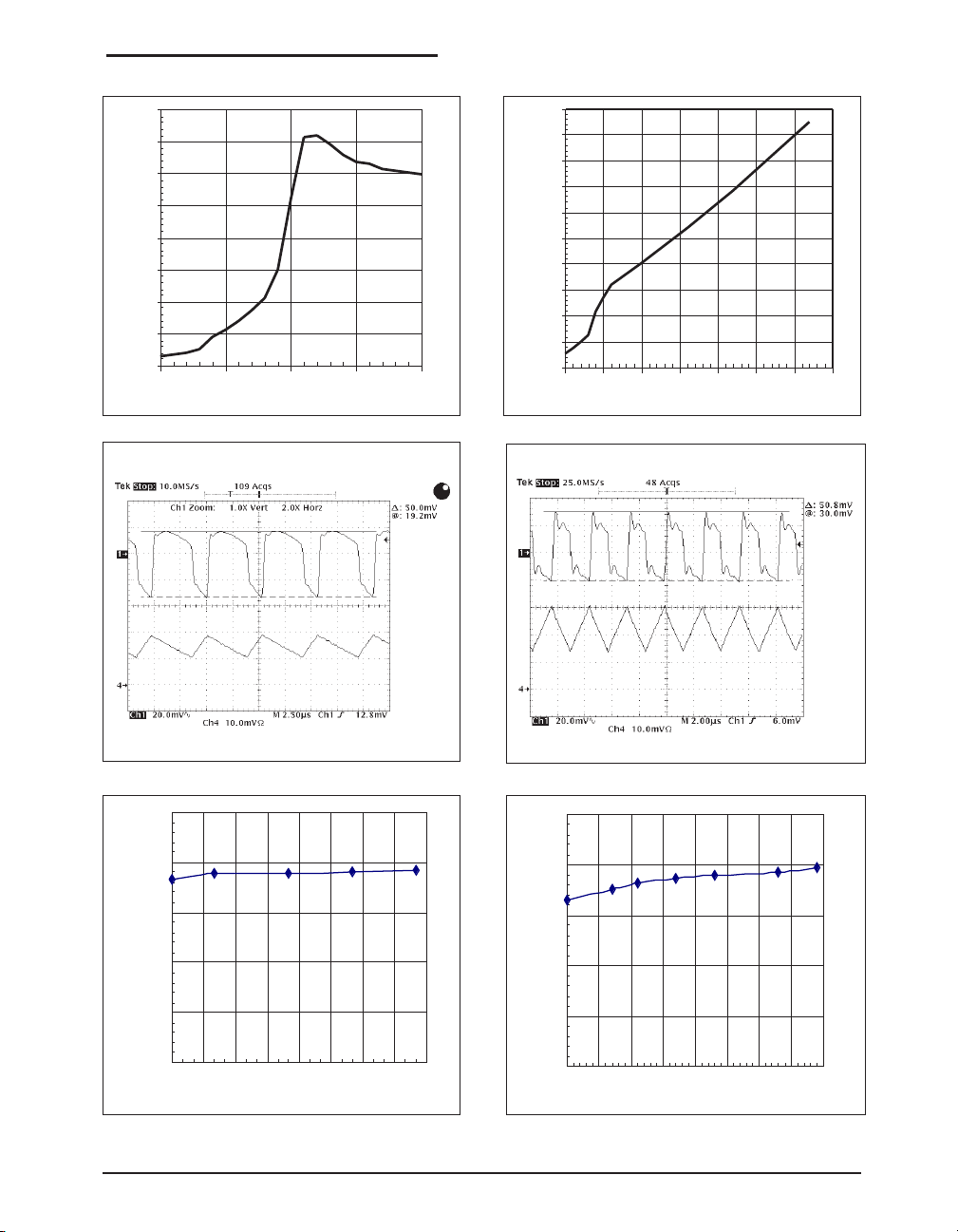
TYPICAL PERFORMANCE CHARACTERISTICS
Refer to the Typical Application Circuit on page 1, T
400
350
300
250
200
Io (mA)
150
100
50
0
1.0 1.5 2.0 2.5 3.0
Maximum Resistive Load Current in Startup, V
Vin (V)
OUT
V
OUT
=3.3V
(AC)
=+25°C.
AMB
500
450
400
350
300
250
Io (mA)
200
150
100
50
0
1.0 1.5 2.0 2.5 3.0 3.5 4.0 4.5
Vin (V)
Maximum Resistive Load Current in Startup, V
OUT
=5.0V
V
OUT
(AC)
=200mA, V
LOAD
Vin (V)
Inductor Current
(0.2A/DIV)
OUT
=5.0V
Inductor Current
(0.2A/DIV)
Output Ripple, VIN=2.6V, I
5.0
4.0
3.0
2.0
Kon (V*usec)
1.0
0.0
0.9 1.2 1.5 1.8 2.1 2.4 2.7 3.0 3.3
KON vs. V
Date: 1/19/05 SP6648 Ultra-low Quiescent Current, High Efficiency Boost Regulator © Copyright 2005 Sipex Corporation
, V
=3.3V KON vs. V
IN
OUT
=200mA, V
LOAD
Vin (V)
OUT
=3.3V
Output Ripple, VIN=2.6V, I
5.0
4.0
3.0
2.0
Kon (V*usec)
1.0
0.0
0.9 1.4 1.9 2.4 2.9 3.4 3.9 4.4 4.9
, V
=5.0V
IN
OUT
7
Page 8
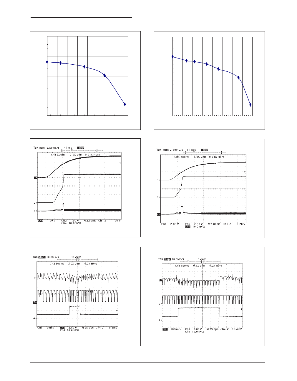
TYPICAL PERFORMANCE CHARACTERISTICS
Refer to the Typical Application Circuit on page 1, T
2.0
AMB
=+25°C.
2.0
1.5
1.0
Koff (V*usec)
0.5
0.0
0.9 1.2 1.5 1.8 2.4 2.7 3.0 3.3
2.1
Vin (V)
K
vs. V
, V
OFF
=3.3V
IN
OUT
V
V
I
IN
IN
OUT
(1A/div)
1.5
1.0
Koff (V*usec)
0.5
0.0
0.9 1.4 1.9 2.4 2.9 3.4 3.9 4.4 4.9
K
vs. V
, V
OFF
=5.0V
IN
OUT
Vin (V)
V
IN
V
OUT
IIN(1A/div)
Startup, VIN=2.6V, V
Load Step, 0.1A to 0.3A, V
=3.3V, R
OUT
= 2.6V, V
IN
LOAD
= 100Ω
= 3.3V
OUT
V
LX
I
OUT
OUT
(AC)
(0.2A/div)
Startup, VIN=4.2V, V
=5.0V, R
OUT
Load Step, 0.3A to 0.5A, V
= 4.2V, V
IN
LOAD
= 100Ω
= 5.0V
OUT
V
OUT
LX
I
OUT
(AC)
(0.5A/DIV)
Date: 1/19/05 SP6648 Ultra-low Quiescent Current, High Efficiency Boost Regulator © Copyright 2005 Sipex Corporation
8
Page 9

APPLICATIONS INFORMATION
Circuit Layout
Printed circuit board layout is a critical part of a
power supply design. Poor designs can result in
excessive EMI on the feedback paths and on the
ground planes with applications involving high
switching frequencies and large peak currents.
Excessive EMI can result in instability or regulation errors. All power components should be
placed on the PC board as closely as possible
with the traces kept short, direct, and wide
(>50mils or 1.25mm). Extra copper on the PC
board should be integrated into ground as a
pseudo-ground plane. On a multilayer PC board,
route the star ground using component-side copper fill, then connect it to the internal ground
plane using vias. For the SP6648 devices, the
inductor and input and output filter capacitors
should be soldered with their ground pins as
close together as possible in a star-ground configuration. The V
pin must be bypassed di-
OUT
rectly to ground as close to the SP6648 devices
as possible (within 0.2in or 5mm). The DC-DC
converter and any digital circuitry should be
placed on the opposite corner of the PC board as
far away from sensitive RF and analog input
stages. Noisy traces, such as from the LX pin,
should be kept away from the voltage-feedback
V
node and separated from it using grounded
OUT
copper to minimize EMI. See the SP6648EB
Evaluation Board Manual for PC Board Layout
design details.
Component Selection
Selection of capacitors for SP6648 power supply circuits can be made through the use of the
Component Selection Table. Capacitor equivalent series resistance (ESR) in the range of 0.2Ω
to 0.3Ω is a requirement for obtaining sufficient
output voltage ripple for the SP6648 to properly
regulate under load. For ESR values in this
range, low ESR Tantalum capacitors are recommended. For example, in the SP6648 application circuit a 47µF, 10V, low-ESR, surfacemount tantalum output filter capacitor typically
provides 50mV output ripple when stepping up
from 2.6V to 3.3V at 200mA. Ceramic capacitors have ESR too low to produce enough output
ripple for the SP6648 to regulate the output.
Designers should select input and output capacitors with a rating exceeding the inductor
current ripple, which is typically set by the
inductor value and the KON value as given in the
following relationship:
I
L(RIPPLE)
= KON/L
For the example of the 10µH inductor the inductor current ripple would be 330mA, while for the
22µH inductor the inductor current ripple value
would be 150mA. Do not allow tantalum capacitors to exceed their ripple-current ratings.
An input filter capacitor can reduce peak currents drawn from the battery and improve efficiency. For most applications, use the same
47µF tantalum capacitor as used for the input.
Low-ESR aluminum electrolytic capacitors are
acceptable provided they meet the ESR requirement of 0.2Ω to 0.3Ω, and we list an appropriate
100µF aluminum electrolytic in the component
selection table, but standard aluminum electrolytic capacitors are not recommended.
In selecting an inductor, the saturation current
specified for the inductor needs to be greater
then the SP6648 peak current to avoid saturating
the inductor, which would result in a loss in
efficiency and could damage the inductor. The
SP6648 evaluation board uses a Sumida
CDRH5D28 10µH inductor with an I
SAT
value
of 1.3A and a DCR of 0.065Ω, which easily
handles the I
of 0.85A of the SP6648 and
PEAK
will deliver high efficiencies. Other inductors
could be selected provided their I
than the I
of the SP6648.
PEAK
is greater
SAT
Date: 1/19/05 SP6648 Ultra-low Quiescent Current, High Efficiency Boost Regulator © Copyright 2005 Sipex Corporation
9
Page 10
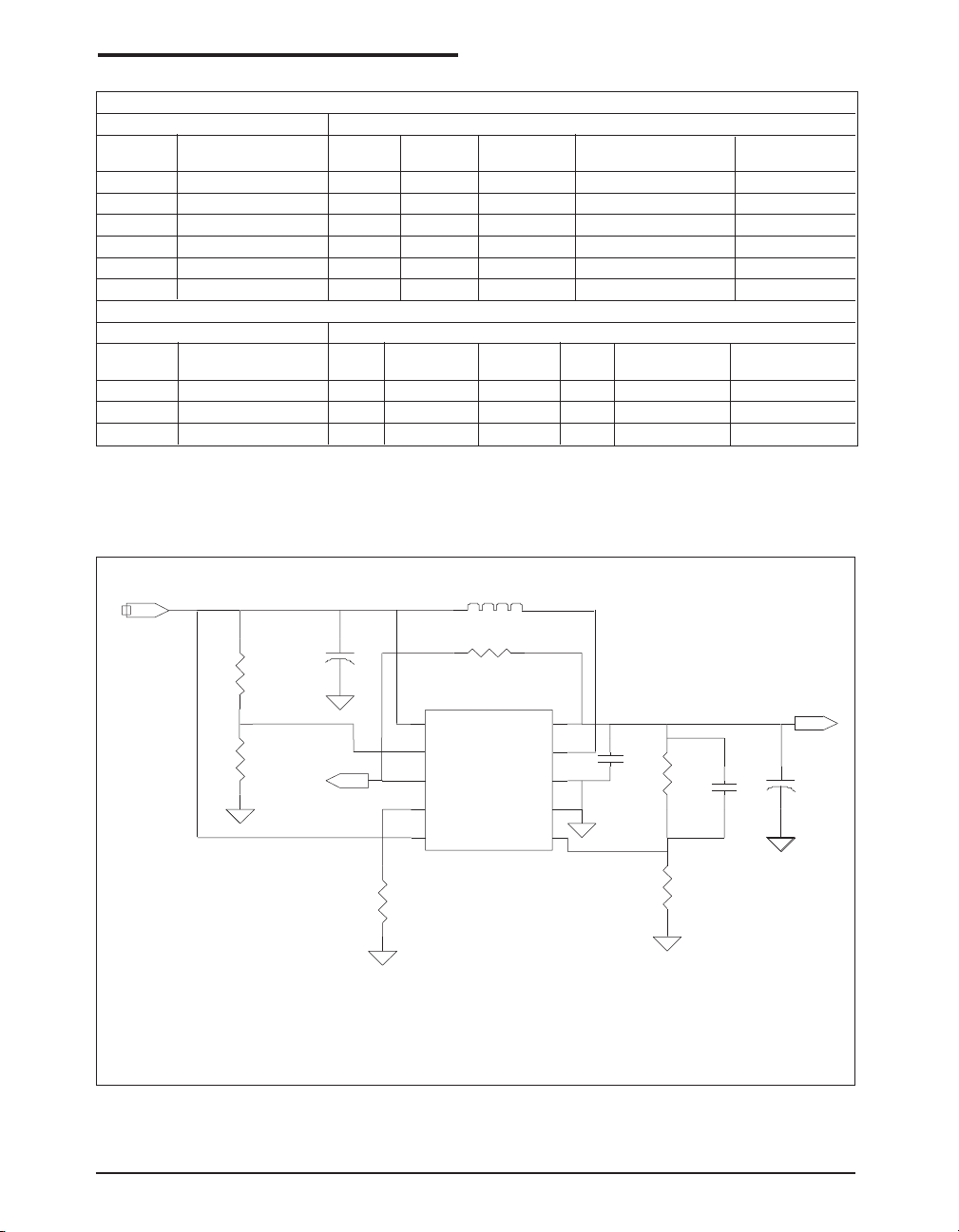
APPLICATIONS INFORMATION: Continued
INDUCTORS - SURFACE MOUNT
Inductor Specification
Inductance Manufacturer/Part No. Series R I
(µH)
10 Sumida CDRH5D28-100 0.065 1.30 5.7x5.5x3.0 Shielded Ferrite Core www.sumida.com
10 TDK RLF5018T-100MR94 0.067 0.94 5.6x5.2x2.0 Shielded Ferrite Core www.tdk.com
10 Sumida CD43-100 0.180 1.04 4.0x4.5x3.5 Unshileded Ferrite Core www.sumida.com
22 Sumida CDRH5D28-220 0.122 0.90 5.7x5.5x3 Shileded Ferrite Core www.sumida.com
22 TDK RLF5018T-220MR63 0.067 0.63 5.6x5.2x2.0 Shielded Ferrite Core www.tdk.com
22 Sumida CD43-220 0.378 0.68 4.0x4.5x3.5 Unshielded Ferrite Core www.sumida.com
Ω
SAT
(A) (mm) Website
CAPACITORS - SURFACE MOUNT & LEADED
Capacitance Manufacturer Part No. ESR Ripple Current Size LxWxH Voltage Capacitor Manufacturer
µ
F)
(
47 Kemet T494C476K010AS 0.300 1.06 6.0x3.2x2.5 10 SMT Tantalum www.kemet.com
47 Kemet T494V476K010AS 0.300 0.99 7.3x4.3x2.0 10 SMT Tantalum www.kemet.com
100 Sanyo 25MV100AX 0.220 0.30 6.3DX11L 25 Radial Al Electrolytic www.sanyovideo.com
Note: Components highlighted in bold are those used on the SP6648EB Evaluation Board.
Ω
(max) (A) @ 85°C (mm) (V) Type Website
Component Selection Table
Size LxWxH Intuctor Type Manufacturer
Capacitor Specification
V
BATT
R
3
549K
R
LBON
4
249K
SP6648EB Evaluation Board Schematic
C1
+
47µF
1
2
3
4
5
R
LIM
1.87K
L1
R51.0M
U1 SP6648
V
BATT
LBI
LBON
R
LIM
SHDN
10µH
P
GND
3.3V
+
47µF
OUT
C2
10
V
OUT
9
LX
GND
FB
C4
8
7
6
1µF
R
205K
R
1
C3
47pF
2
124K
Date: 1/19/05 SP6648 Ultra-low Quiescent Current, High Efficiency Boost Regulator © Copyright 2005 Sipex Corporation
10
Page 11

V
Programming
OUT
The SP6648 can be programmed as either a
voltage source or a current source. To program
the SP6648 as voltage source, the SP6648 requires 2 feedback resistors R1 & R2, as shown
in the SP6648EB evaluation board schematic, to
control the output voltage. To set V
OUT
in the
voltage mode, use the equation:
R1 = [(V
/1.25)-1] * R2
OUT
APPLICATIONS INFORMATION : Continued
output goes low as determined by the relationship:
V
LOWBATT
= 0.61 * [(R3 + R4)/R4]
The SP6648 evaluation board R3 & R4 resistors
have been set to trip for a falling battery threshold of about 2.0V. Using this relationship, other
low battery threshold values can be set by the
user.
Using the R
The peak inductor current, I
externally by the R
tween the R
Function
LIM
, is programmed
PEAK
resistor connected be-
LIM
pin and GND. The peak inductor
LIM
current is defined by:
I
= 1600/R
PEAK
LIM
The saturation current specified for the inductor
needs to be greater than the peak current to avoid
saturating the inductor, which would result in a
loss in efficiency and could damage the inductor. The SP6648 evaluation board uses a R
value of 1.87K for an I
= 850mA to allow
PEAK
LIM
the circuit to deliver up to 180mA for 1.3V input
and 400mA for 2.6V input. Other values could
be selected using the above relationships.
Using the LBON - Low Battery Output
Function
The SP6648 will regulate the output until the
input battery is completely discharged or until
the under voltage lock-out (UVLO) occurs at
V
= 0.61V. To provide a low battery warn-
BATT
ing, the Low Battery Output function of the
SP6648 can be used. LBON is programmed
externally by the R3 and R4 resistor divider
connected between V
, the LBI input pin
BATT
and GND. The LBON is an open drain output,
which is active low and is pulled up by a 1M
resistor R5 to V
. When the LBI comparator
OUT
falling threshold of 0.61V is reached, the LBON
UVLO the Under Voltage Lock-Out Function
Once started up, the SP6648 will regulate the
output until the input battery is completely discharged or until the under voltage lock-out
(UVLO) occurs at V
= 0.61V. The UVLO
BATT
function will completely open all switches until
the battery again rises above the 0.61V threshold.
Maximum Startup Current
It should be noted that for low input voltages the
SP6648 startup circuit can not support large
load currents at startup. In startup the SP6648
needs to boost the output from zero volts using
the input voltage. Once the output is greater than
1.9V the operate circuit takes over and the
SP6648 can supply much more current. Curves
of maximum load current in startup for the
SP6648 are shown in the typical performance
characteristics and can be compared with the
page one curve for maximum load current in
operation.
For 1-cell battery applications, it is recommended
to apply any large load current after the SP6648
has started up, typically in a few milliseconds.
This is typically not a problem in many applications where the load is a processor whose load
current is low until the processor voltage comes
up.
Date: 1/19/05 SP6648 Ultra-low Quiescent Current, High Efficiency Boost Regulator © Copyright 2005 Sipex Corporation
11
Page 12
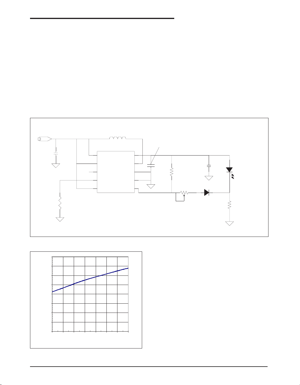
APPLICATIONS INFORMATION
SP6648LEDEB Evaluation Board with
LumiLED High Brightness White LED
For the high brightness LumiLED white LED
application, the SP6648 is generally programmed
as a current source. The bias resistor R
is used
b
to set the operating current of the white LED as
equation:
R
= V
b
REF/IF
V
BATT
1.8-3.2V
C1
10µF
R
LIM
1.87K
L1
10µH
1
V
BATT
2
SP6648
LBI
3
LBON
4
R
LIM
5
SHDN
V
P
GND
GND
OUT
LX
FB
10
9
8
7
6
where V
is around 0.61V, IF is the operating
REF
current of the LumiLED. To set the operating
current to be about 350mA, Rb is selected as 1.8 Ω
as shown in the following schematic. The efficiency of the SP6648 LumiLED circuit is improved by the use of a silicon diode D1 and
resistor R1 to set the voltage at the current sense
resistor R2 to 0.61V instead of the higher 1.25V
at the FB pin. An efficiency curve follows
showing the SP6648 efficiency driving 350mA
output current into the high brightness LumiLED.
Important:
1µF Ceramic Cap at V
needed for stable regulation
C4
1µF
R
1
16.2k
OUT
10K
R
5
(R5 optional)
I
=0.61V/R
OUT
Pin
D1 1N4148
C2
10µF
b
D2
1W LED
350mA
V
REF
Rb
1.8Ω
= 0.61V
SP6648LEDEB Evaluation Board Schematic
100
95
90
85
80
75
Efficiency (%)
70
65
60
1.8 2.0 2.2 2.4 2.6 2.8 3.0 3.2
Battery Voltage (V)
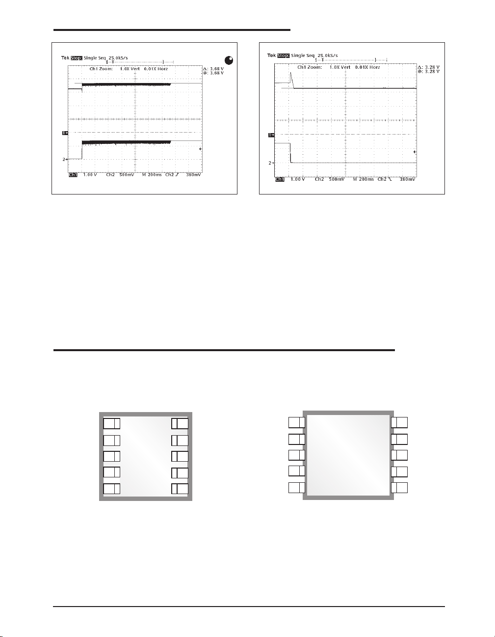
As shown in following scope photos, if the
SP6648 is powered up before the LumiLED is
plugged in, the circuit will bring the Feedback
pin to 0V and the SP6648 has a feature to set the
output voltage to be 3.3V. Once the LumiLED is
plugged in, the Feedback pin will go up to 1.25V
and begin to regulate. The output voltage will go
from 3.3V to 3.68V (=VF+0.61V), where VF is
the forward voltage of the LumiLED. When the
LumiLED is open, the Feedback pin voltage
will go to 0V and the output voltage will go to
3.3V which will protect the part.
SP6648LEDEB Efficiency Curve
Date: 1/19/05 SP6648 Ultra-low Quiescent Current, High Efficiency Boost Regulator © Copyright 2005 Sipex Corporation
12
Page 13
APPLICATIONS INFORMATION
V
OUT
V
REF
V
OUT
V
REF
Plug in the LumiLED
Brightness Control
One approach to control LED brightness is to
apply a PWM signal to the SHDN input of the
SP6648. In this case, the output current will be
equal to the product of 350mA and the average
duty cycle at the SHDN pin. An optional 10K
potentiometer (R5) may also be used for dimming the LED current by varying the potentiometer between low brightness and full brightness.
V
BATT
LBON
R
LIM
SHDN
LBI
1
2
3
4
5
SP6648
10 Pin DFN
10
V
OUT
9
LX
8
P
GND
7
GND
6
FB
Unplug the LumiLED
V
1
BATT
LBI
2
LBON
3
4
5
10 Pin MSOP
R
LIM
SHDN
SP6648
PINOUTS
10
V
OUT
9
LX
8
P
V
GND
7
GND
6
FB
Date: 1/19/05 SP6648 Ultra-low Quiescent Current, High Efficiency Boost Regulator © Copyright 2005 Sipex Corporation
13
Page 14
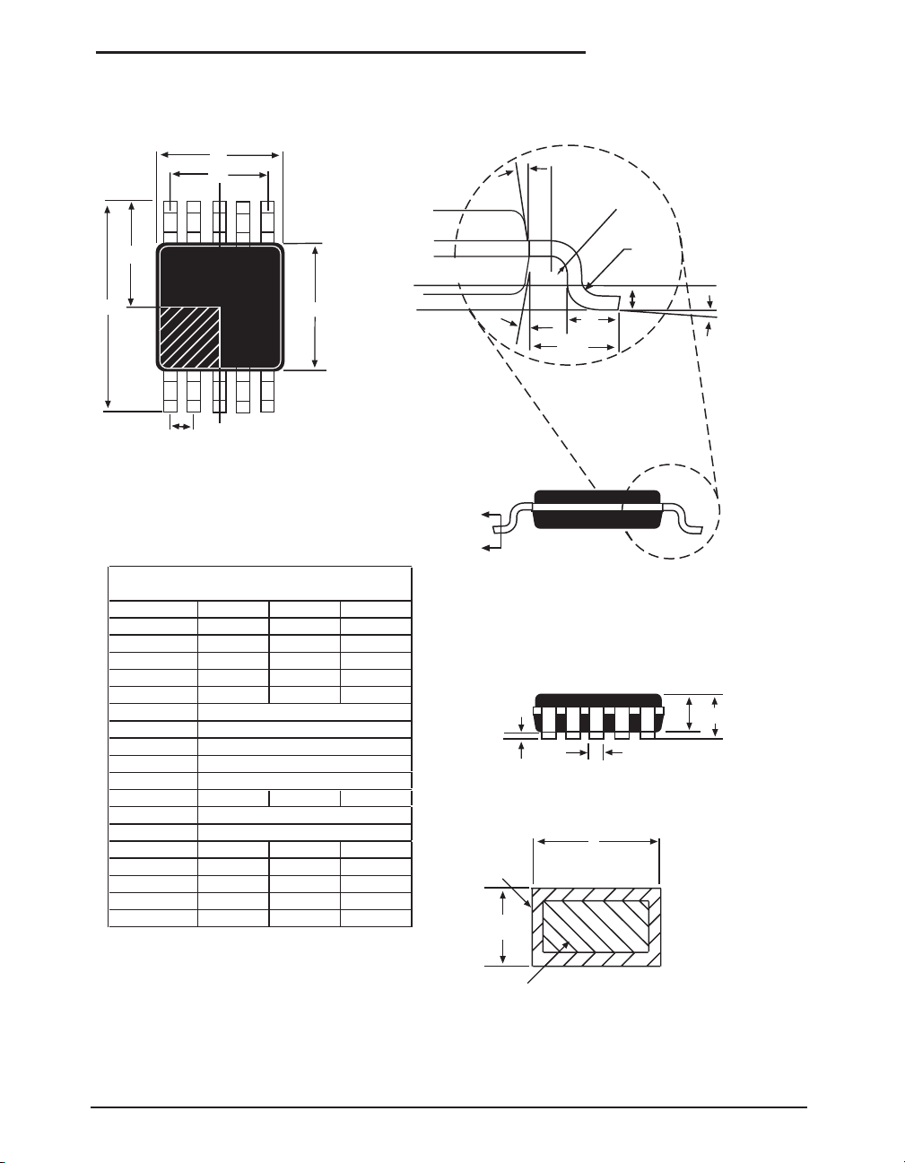
PACKAGE: 10 PIN MSOP
D
e1
Ø1
R1
E/2
E
1
2
E1
Seating Plane
e
Pin #1 indentifier must be indicated within this shaded area (D/2 * E1/2)
10 Pin MSOP JEDEC MO-187 (BA) Variation
SYMBOL
MIN NOM MAX
A--1.1
A1 0 - 0.15
A2 0.75 0.85 0.95
b 0.17 - 0.27
c 0.08 - 0.23
D
E
E1
e
e1
3.00 BSC
4.90 BSC
3.00 BSC
0.50 BSC
2.00 BSC
L 0.4 0.6 0.8
L1
L2
0.95 REF
0.25 BSC
N-10R 0.07 - -
R1 0.07 - -
ø0º-8º
ø1 0º - 15º
Note: Dimensions in (mm)
Ø1
B
B
WITH PLATING
c
R
A2
Gauge Plane
Ø
A
L2
L
L1
b
A1
b
1
Date: 1/19/05 SP6648 Ultra-low Quiescent Current, High Efficiency Boost Regulator © Copyright 2005 Sipex Corporation
BASE METAL
Section B-B
14
Page 15
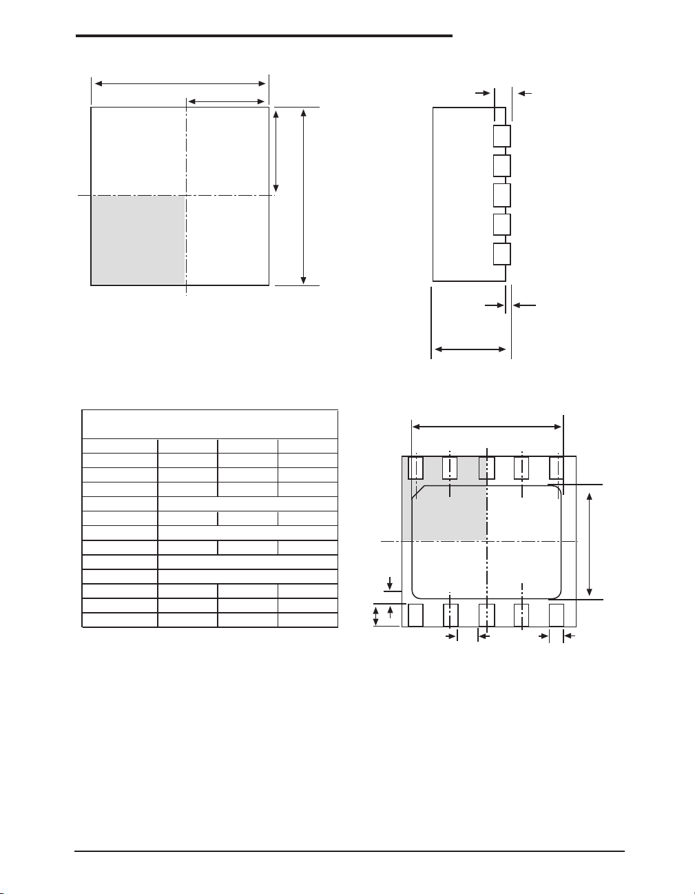
D
Top View
D/2
PACKAGE: 10 PIN DFN
A3
E/2
E
A1
A
Side View
3x3 10 Pin DFN JEDEC MO-229 (VEED-5)
VARIATION
SYMBOL
MIN NOM MAX
A 0.8 0.9 1
A1 0 0.02 0.05
A2 0.55 0.65 0.8
A3
0.20 REF
b 0.18 0.25 0.3
D
3.00 BSC
D2 2.2 2.7
e
E
0.5 PITCH
3.00 BSC
E2 1.4 - 1.75
K 0.2 - -
L 0.3 0.4 0.5
Note: Dimensions in (mm)
D2
2
1
E2
K
L
e
b
Bottom View
Date: 1/19/05 SP6648 Ultra-low Quiescent Current, High Efficiency Boost Regulator © Copyright 2005 Sipex Corporation
15
Page 16
ORDERING INFORMATION
Part Number Top Mark Operating Temperature Range Package Type
SP6648EU ................................ SP6648EU..................-40°C to +85°C ...................................... 10 Pin MSOP
SP6648EU/TR .......................... SP6648EU..................-40°C to +85°C..................................... 10 Pin MSOP
SP6648ER ............................... SP6648ERYWW..........-40°C to +85°C ........................................ 10 Pin DFN
SP6648ER/TR ......................... SP6648ERYWW..........-40°C to +85°C ....................................... 10 Pin DFN
Available in lead free packaging. To order add "-L" suffix to part number.
Example: SP6648EU/TR = standard; SP6648EU-L/TR = lead free
/TR = Tape and Reel
Pack quantity is 2,500 for MSOP and 3,000 for DFN.
CLICK HERE TO ORDER SAMPLES
Corporation
ANALOG EXCELLENCE
Sipex Corporation
Headquarters and
Sales Office
233 South Hillview Drive
Milpitas, CA 95035
TEL: (408) 934-7500
FAX: (408) 935-7600
Sipex Corporation reserves the right to make changes to any products described herein. Sipex does not assume any liability arising out of the
application or use of any product or circuit described herein; neither does it convey any license under its patent rights nor the rights of others.
Date: 1/19/05 SP6648 Ultra-low Quiescent Current, High Efficiency Boost Regulator © Copyright 2005 Sipex Corporation
16
 Loading...