

Page 1
®
SP6683
1.5x Charge Pump LED Driver for Parallel Configuration
FEATURES
■ 200mA Output Using 1µF Ceramic Caps
■ Drives up to 8 white LED's
■ 0.5µA Shutdown Current
■ 1x/1.5x Mode Charge Pump
■ +2.7V to +5.5V Input Voltage Range
■ Built-in 1.2MHz Oscillator
V
V
MODE
OUT
C1P
V
FB
1
2
SP6683
3
IN
10 Pin DFN
4
5
10
9
8
7
6
C2P
C1N
GND
C2N
EN/PWM
■ 0.5mA Quiescent Current
■ Programmable Output Current or Voltage
■ PWM Dimming Control via Enable Pin
■ Soft Start to limit In-Rush Current
■ Space Saving 10-pin 3 x 3mm DFN Package
■ Three Options for Optimizing Efficiency:
■ SP6683 - MOSFET discharge in shutdown
■ SP6683-03 - High Impedance in shutdown
■ SP6683-LV - Low Voltage (150mV)V
ence
Now Available in Lead Free Packaging
APPLICATIONS
■ Mobile Phone
■ Camera Flash Driver
■ PDA
■ Digital Still Camera
Refer-
FB
■ Digital Camcorder
■ Color LCD Module
DESCRIPTION
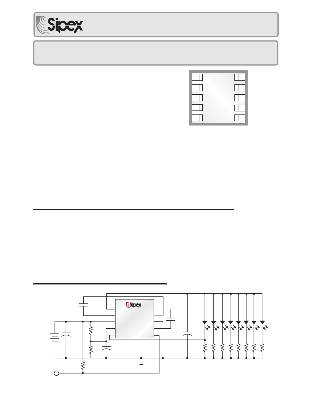
The SP6683 is a high power current regulated charge pump ideal for converting a Li-Ion
battery input for driving up to 8 white LED’s used in backlighting color displays. The SP6683
operates with an internal 1.2MHz clock, enabling the use of small external components.
Output current can be accurately regulated by modulating the switcher between the charge
pump and output capacitor. In shutdown mode, the SP6683 discharges the output to ground
and draws less than 500nA current. The SP6683 utilizes 1µF capacitors to deliver up to
200mA current regulated WLED drive capability. The SP6683 family includes three options
that allow the user to optimize LED driving circuit; SP6683-LV with low voltage reference,
SP6683-03 with high impedance output in shutdown, and SP6683 with pulled down output
in shutdown. The SP6683 is offered in 10-pin DFN package.
TYPICAL APPLICATION SCHEMATIC
SP6683
®
C2P
C1N
GND
C2N
EN/PWM
10
9
8
7
6
C4
1µF
C5
1µF
White
LED
C2
1µF
R5
1M
R1
R2
R2
Lithium-Ion
ENABLE/PWM DIMMING
Date: 08/24/04 SP6683 1.5X Charge Pump LED Driver for Parallel Configuration © Copyright 2004 Sipex Corporation
C1
1µF
1
2
3
4
5
C3
1µF
V
C1P
V
V
FB
OUT
IN
MODE
1
Page 2
ABSOLUTE MAXIMUM RATINGS
VIN, V
Output Current (I
Power Dissipation per Package - 10-pin DFN
(derate 8.84mW/°C above +70°C) ..................... 1.2W
Junction Temperature.................................... +125°C
Storage Temperature ...................... -65°C to +150°C
ESD Rating................................................. 2kV HBM
MODE
, V
and EN/PWM.................-0.3V to 6V
OUT
) ...................................... 300mA
OUT
These are stress ratings only and functional operation of
the device at these ratings or any other above those
indicated in the operation sections of the specifications
below is not implied. Exposure to absolute maximum
rating conditions for extended periods of time may affect
reliability.
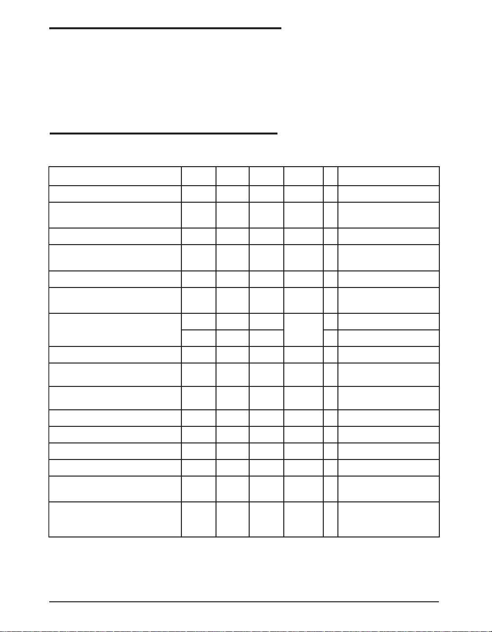
ELECTRICAL CHARACTERISTICS
Unless otherwise specified: VIN = 3.6V, C1=C2=C4=C5=1.0µF (Ceramic, ESR=0.03 Ω) and T
specifications which apply over full operating temperature range -40ºC to +85ºC.
retemaraP.niM.pyT.xaMstinUsnoitidnoC
=25°. The ♦ denotes
AMB
egatloVtupnI7.25.5V
tnerruCtnecseiuQ5.03 Am
tnerruCnwodtuhS5.05.1Aµ
tnerruCdaoLmumixaM002
ycneuqerFrotallicsO7.02.15.1zHM
V
BF
egatloVecnerefeR382.0513.0743.0V
831
ecnatsiseRtuptuO
36
V
EDOM
V
EDOM
V
EDOM
egatloVdlohserhT00.152.105.1VVNIgnillaF
siseretsyH03Vm
tnerruCniP10.05.0Aµ
woLcigoLMWP/NE4.0V
hgiHcigoLMWP/NE6.1V
tnerruCniPMWP/NE10.05.0Aµ
tnerruCniPBF10.05.0Aµ
V
elppiR08Vm
TUO
♦
V
NI
♦
♦
V
NE
V
Am
NI
♦
V
NI
I
TUO
♦
♦
♦
♦
V
EDOM
V,V5.5-0.3=
=
TUO
Aµ001=tuoI,V6.3
V,V0=MWP/
V5.5=
NI
V6.3=tuoV,V2.4=
V5.5-7.2=
V,Am02=
edoMX5.1
,V6.3=
TUO
daoLAm001,edoMX5.1
daoLAm001,edoMX0.1
V52.1=
♦
♦
♦
V
NE
♦
VBFV1=
V
TUO
V2.4=MWP/
I,V4=
TUO
edoMx5.1,
Am001=
noitaluger%09gnihtiwBF
V
TUO
emiTnO-nruT052005sµ
♦
I
TUO
V,edoMX5.1
Aµ001=
,6.3=
TUO
Date: 08/24/04 SP6683 1.5X Charge Pump LED Driver for Parallel Configuration © Copyright 2004 Sipex Corporation
2
Page 3
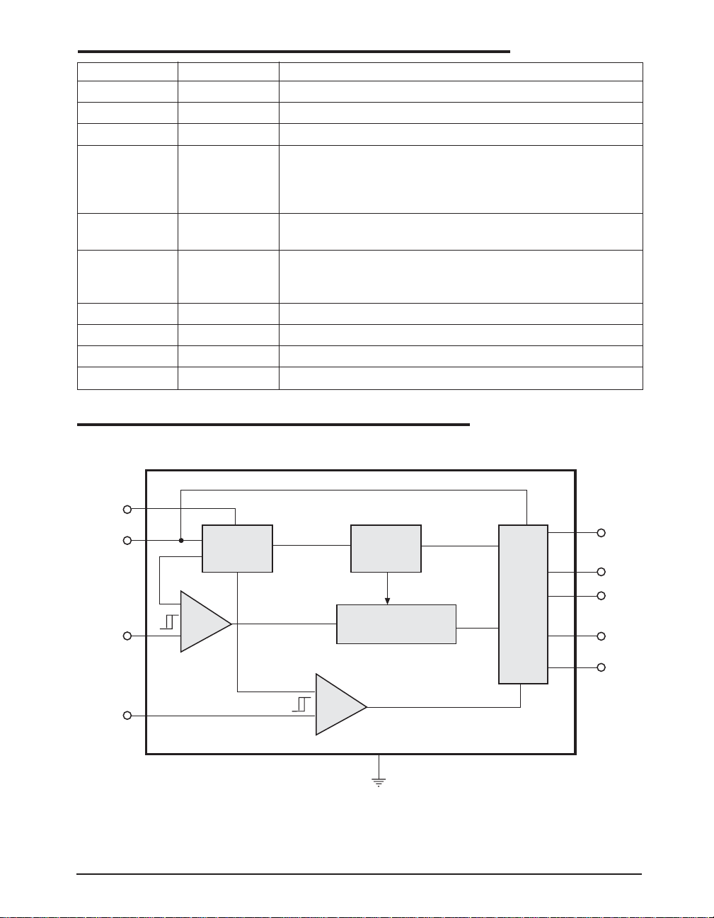
PIN DESCRIPTION
PIN NUMBER PIN NAME DESCRIPTION
1V
OUT
Regulated charge pump output.
2 C1P Positive terminal to the charge pump flying capacitor C2.
3VINInput supply voltage.
4V
MODE
Charge pump mode program pin. When V
is greater than 1.25V,
MODE
a X1 charge pump is used. Otherwise, charge pump switches to X1.5
mode. A voltage divider shown in the typical application circuit
programs the VIN threshold for charge pump mode switching.
5FBThis is the feedback pin for output current or voltage regulation. The
voltage of this pin is compared with an internal 315mV reference.
6 EN/PWM Enable and PWM dimming control input. Pull this pin low to discon-
nect V
from VIN and shutdown the SP6683.V
OUT
is pulled to
OUT
ground in shutdown.
7 C2N Negative terminal to the charge pump flying capacitor, C4.
8 GND Ground reference.
9 C1N Negative terminal to the charge pump flying capacitor, C2.
10 C2P Positive terminal to the charge pump flying capacitor C4.
FUNCTIONAL DIAGRAM
V
IN
EN/PWM
V
MODE
FB
1.25V
MODE
COMP
Voltage
Reference
315mV
V
OUT
COMP
1.2 MHz
Clock
Manager
Mode Control
Start-up
and
Charge
Pump
Switches
C1P
C1N
C2P
C2N
V
OUT
GND
Date: 08/24/04 SP6683 1.5X Charge Pump LED Driver for Parallel Configuration © Copyright 2004 Sipex Corporation
3
Page 4
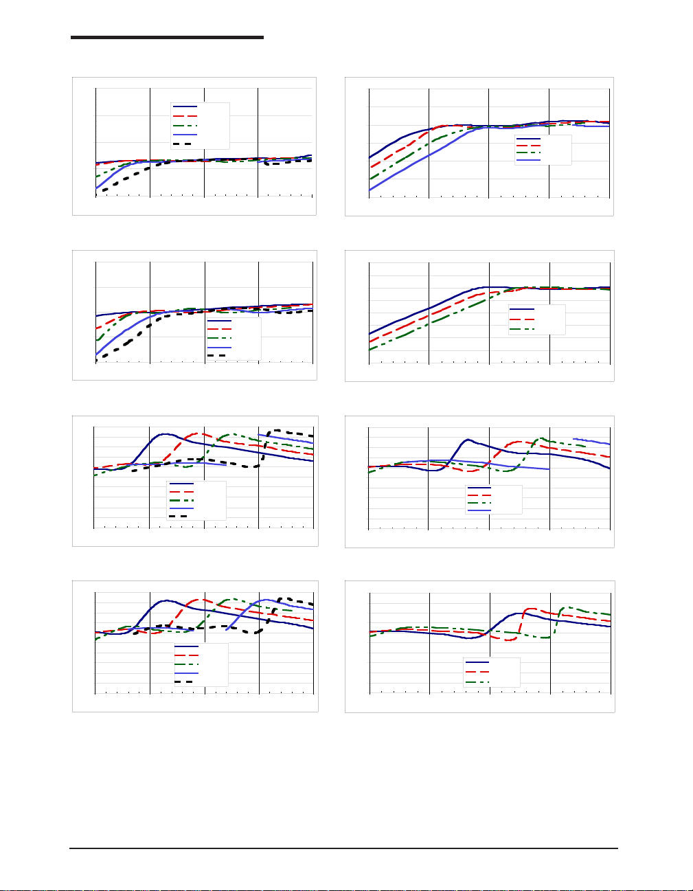
TYPICAL PERFORMANCE CHARACTERISTICS (25ºC)
200
150
100
Iout (mA)
50
0
3.0 3.5 4.0 4.5 5.0
200
150
100
Iout (mA)
50
0
3.0 3.5 4.0 4.5 5.0
100
90
80
70
60
50
40
Efficiency (%)
30
20
10
0
3.0 3.5 4.0 4.5 5.0
Iout vs. Vin @ 60mA
Vf = 3.0V
Vf = 3.3V
Vf = 3.6V
Vf = 3.9V
Vf = 4.2V
Vin (V)
Iout vs. Vin @ 100mA
Vf = 3.0V
Vf = 3.3V
Vf = 3.6V
Vf = 3.9V
Vf = 4.2V
Vin (V)
Efficiency vs Vin (Iout = 60mA)
Vf = 3.0V
Vf = 3.3V
Vf = 3.6V
Vf = 3.9V
Vf = 4.2V
Vin (V)
300
250
200
150
Iout (mA)
100
50
0
3.0 3.5 4.0 4.5 5.0
400
350
300
250
200
Iout (mA)
150
100
50
0
3.0 3.5 4.0 4.5 5.0
100
90
80
70
60
50
40
Efficiency (%)
30
20
10
0
3.0 3.5 4.0 4.5 5.0
Iout vs. Vin @ 200mA
Vin (V)
Iout vs. Vin @ 300mA
Vin (V)
Efficiency vs Vin (Iout = 200mA)
Vf = 3.0V
Vf = 3.3V
Vf = 3.6V
Vf = 3.9V
Vin (V)
Vf = 3.0V
Vf = 3.3V
Vf = 3.6V
Vf = 3.9V
Vf = 3.0V
Vf = 3.3V
Vf = 3.6V
100
90
80
70
60
50
40
Efficiency (%)
30
20
10
0
3.0 3.5 4.0 4.5 5.0
Efficiency vs Vin (Iout = 100mA)
Vf = 3.0V
Vf = 3.3V
Vf = 3.6V
Vf = 3.9V
Vf = 4.2V
Vin (V)
100
90
80
70
60
50
40
Efficiency (%)
30
20
10
0
3.0 3.5 4.0 4.5 5.0
Efficiency vs Vin (Iout = 300mA)
Vf = 3.0V
Vf = 3.3V
Vf = 3.6V
Vin (V)
Date: 08/24/04 SP6683 1.5X Charge Pump LED Driver for Parallel Configuration © Copyright 2004 Sipex Corporation
4
Page 5
General Overview
OPERATION
The SP6683 is a current regulated charge pump
ideal for converting a Li-Ion battery input for
driving white LEDs used in backlighting color
displays in cellular phones, PDAs, digital cameras and MP3 players. The SP6683 is able to
efficiently drive up to eight 20mA white LEDs
in parallel and maintain a constant brightness
over a very wide operating voltage range (2.7V
to 5.5V). The SP6683 operates with an internal
1.2MHz clock, enabling the use of small external components. Other features of SP6683 include PWM dimming control as well as complete input/output disconnect in shutdown. In
shut down mode the IC typically draws 500nA
current. The output regulation is achieved by
sensing the voltage at the feedback pin and
modulating the switch between the charge pump
and output capacitor.
Theory of Operation
The SP6683 regulated charge pump block diagram consists of four main blocks (Voltage
Reference, Mode Control, Clock Manager, Startup and Charge-Pump Switches) and two comparators (V
Comparator and V
MODE
OUT
Com-
parator).
1) Voltage Reference. This block provides the
315mV and 1.25V reference voltages needed
for the two comparators.
2) Mode Control. An external voltage divider
connected to the V
pin will define an input
MODE
voltage to the mode comparator which sets the
logic state of the mode selection outputs to the
X1 or X1.5 modes. V
is compared to a
MODE
1.25V bandgap voltage. For example, if one
makes a 158K/100K divider, the mode will
change at 2.58 x 1.25 V =3.23V. A comparatorbased cycle by cycle regulation ensures that no
mode change occurs during cycles.
3) Clock Manager. An internal 1.2MHz clock
is generated in this block. Depending on the
mode control, the appropriate clock phasing is
generated here and sent to the start-up and
charge-pump switches block.
4) V
Comparator and Output Control. A
OUT
315mV reference voltage is compared to feedback voltage to control the Vout needed for the
application. Output current is set by a bias
resistor from the FB pin to the GND pin chosen
by the relationship:
V
=
R
FB
FB
I
OUT
where VFB = 315mV.
Configuring the SP6683 as Voltage or
Current Source
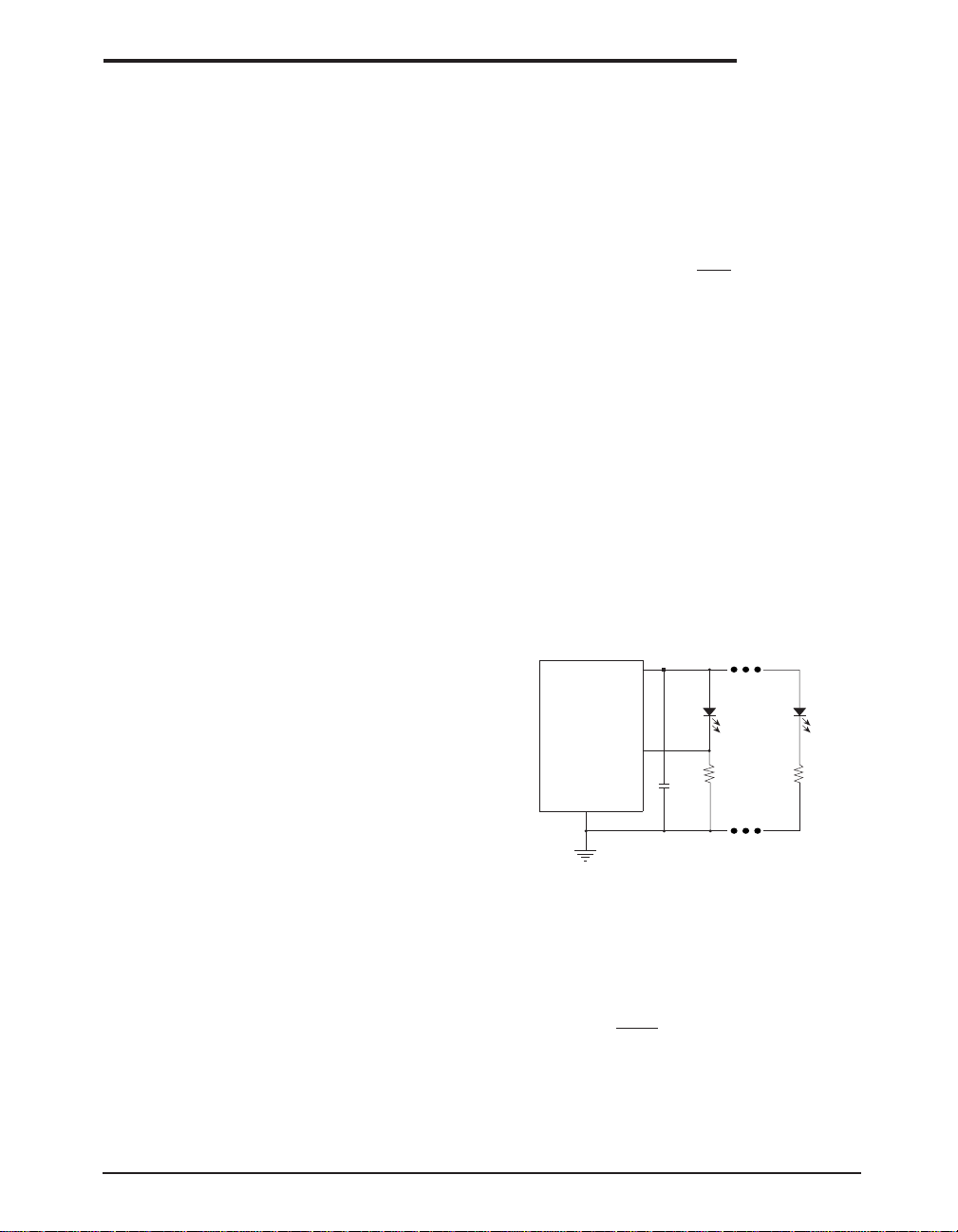
The white LED load configuration used by
customers can be discrete white LEDs or a white
LED module. Inside the white LED module,
there may or may not be resistors in series with
the white LEDs. According to the different
application requirements, the SP6683 can be
configured as either a voltage source or a current
source to provide solutions for these different
applications, as shown in figures 9-12. Figure 9
shows the SP6683 driving discrete white LEDs
as a current source.
V
OUT
1
SP6683
5
FB
Rb
GND
8
Figure 9. Driving discrete white LEDs as current source
1uF
Rb
The current in one white LED current is set by
the ratio of the feedback pin voltage (315mV)
and the bias resistor RB. To set the operating
current, RB can be selected by:
V
RB =
I
FB
LED
The current of the remaining white LEDs is set
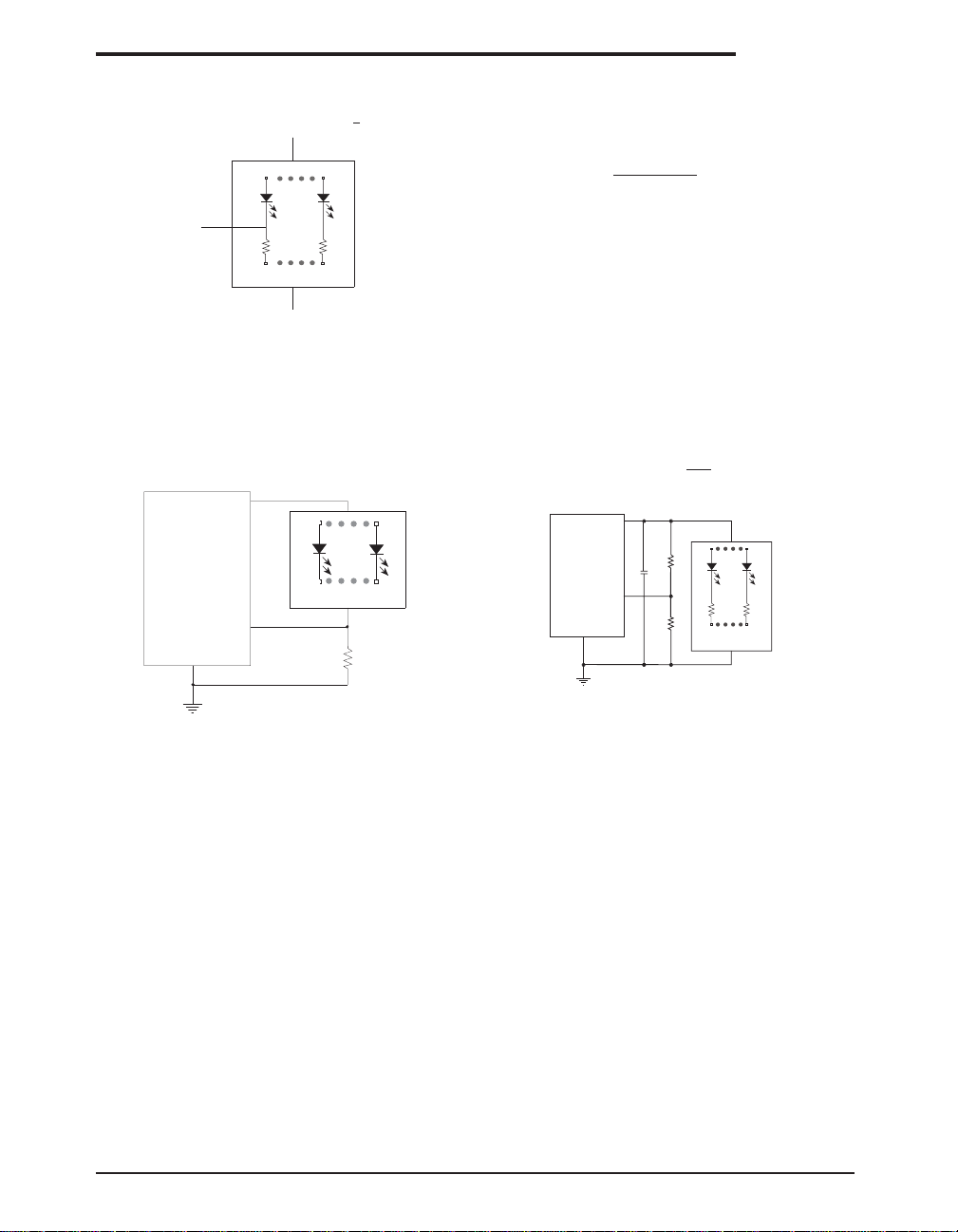
according to the similarity of the white LEDs. 3wire white LED modules with internal series
Date: 08/24/04 SP6683 1.5X Charge Pump LED Driver for Parallel Configuration © Copyright 2004 Sipex Corporation
5
Page 6
OPERATION
Anode
5
8
SP6683
Cathode
V
OUT
R6
1
R5
1uF
V
FB
2-wire W-LED
module
GND
resistors (as shown in figure 10) can also be
driven in this way.
Fig 10. 3-wire white LED module
Anode
FB
3-wire W-LED module
GND
In figure 11, SP6683 was used to drive a 2-wire
white LED module (without internal series resistors) as a current source. The bias resistor R
is selected to regulate the total current of the
white LED module instead of the current of a
single LED as in figure 9.
Anode
Cathode
Rb
SP6683
GND
8
V
OUT
1
2-wire W-LED module
5
V
FB
In this application, the bias resistor can be selected by:
V
FB
=
LED (TOTAL)
is the total operating current
where I
R
B
I
LED(TOTAL)
of all the white LEDs.
To use SP6683 as a voltage source for fixed
voltage applications, a voltage divider is need to
program the output voltage, as shown in figure 12.
The output voltage is set by the ratio of the two
resistors and the feedback control voltage as
shown by:
B
R
V
OUT
= ( 1 +
R
5
) • V
6
FB
Figure 11. Driving 2-wire white LED module as current
source
Date: 08/24/04 SP6683 1.5X Charge Pump LED Driver for Parallel Configuration © Copyright 2004 Sipex Corporation
Figure 12. Driving 2-wire white LED module as
voltage source
6
Page 7
Programming The Operating Mode
g
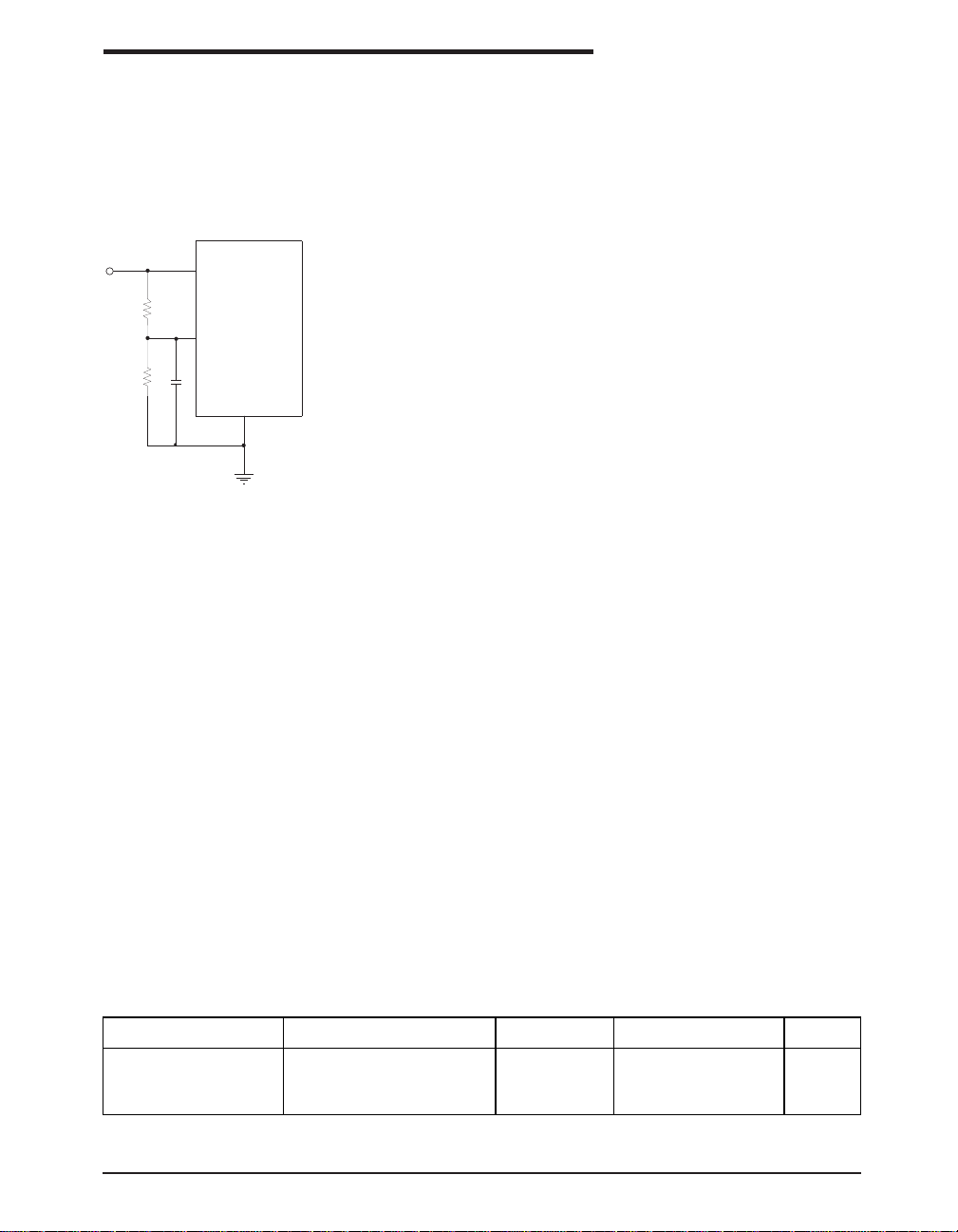
The SP6683 can automatically change from X1
mode to X1.5 to maximize efficiency. To use
this feature, divider resistors should be chosen
according to the specific application, as shown
in figure 13.
APPLICATION INFORMATION
Which can be expressed as R
R1 = [(VTH/1.25) - 1] R
2
1:
V
IN
Figure 13. Programming the Vmode Resistors
3
V
IN
R1
R2
C2
SP6683
4
V
MODE
GND
8
The guideline for divider resistor selections is as
follows. For high input voltage, the SP6683 will
work in X1 mode. When the input voltage drops
to Vth threshold voltage, it will switch to X1.5
mode automatically. The Vth threshold voltage
for mode change can be calculated by:
VTH = (VF + 0.315 + m • I
LED
• R
OUT
)
Where VF and m are the forward voltage and
number of the white LEDs, Rout is the output
resistance of the SP6683.
The equation for the voltage divider R1 and R
with V
MODE
= 1.25V is:
VTH = 1.25V • (1+R1/R2)
For the typical SP6683 application, using VF =
3.6V, m = 8, I
LED =
15mA, R
OUT
= 6Ω, V
be 4.63V, Select R2 = 100kΩ, then R1 = 270kΩ
Capacitor Selection
Ceramic capacitors are recommended for their
inherently low ESR, which will help produce
low peak to peak output ripple, and reduce high
frequency spikes.
The fly capacitor controls the strength of the
charge pump. Selection of the fly capacitor is a
trade-off between the output voltage ripple and
the output current capability. Decreasing the fly
capacitor will reduce the output voltage ripple
because less charge will be delivered to the
output capacitor. However, a smaller fly capacitor leads to larger output resistance, thus decreasing the output current capability and the
circuits efficiency. Increasing the value of the
input and output capacitors could further reduce
the input and output ripple. For peak performance, place all capacitors as close to the SP6683
2
as possible.
Refer to table 1 for some suggested low ESR
capacitors.
TH
will
Table: 1
SUGGESTED LOW ESR CAPACITORS
Manufacturers/ Website Part Number Capacitance/
TDK/www.tdk.com C1005X5R0J105M 1uF/6.3V 0402/X5R/0.5mm 0.03
TDK/www.tdk.com C1608X5R0J225K 2.2uF/6.3V 0603/X5R/0.9mm 0.02
Murata/www.murata.com GRM155R60J105KE19B 1uF/6.3V 0402/X5R/0.55mm 0.03
Murata/www.murata.com GRM188R61A225KE34B 2.2uF/6.3V 0603/X5R/0.9mm 0.02
Date: 08/24/04 SP6683 1.5X Charge Pump LED Driver for Parallel Configuration © Copyright 2004 Sipex Corporation
Volta
e
Capacitor
Size/Type/Thickness
7
ESR at
100KHz
Page 8
Brightness Control Using PWM
Dimming control can be achieved by applying
a PWM control signal to the EN/PWM pin.
The brightness of the white LEDs are controlled by increasing and decreasing the duty
cycle of the PWM signal. While operating
frequency range is from 60Hz to 700Hz, the
recommended maximum brightness frequency
range is from 60Hz to 200Hz. A repetition rate
of at least 60Hz is required to prevent flicker.
Brightness Matching
For white LEDs, the forward voltage drop is a
function of the operating current. However,
for a given current, the forward voltage drop
across each LED does not always match exactly. This can cause uneven brightness in the
white LEDs.
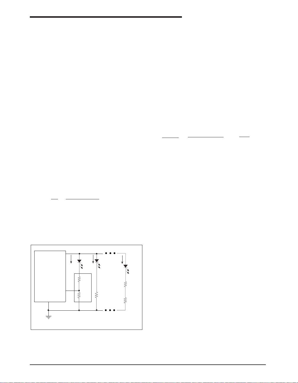
In figure 14, assuming high-precision bias
resistors were used, the operating current ratio
of two different branches can be easily derived
as shown by:
APPLICATION INFORMATION
Since the brightness of the white LED is proportional to the operating current, for better brightness matching, a higher output voltage could be
used. This could be done by using a larger resistor, as shown in figure 14. Rb2 is used to bias the
operating current of the white LED, Rb1 is use to
increase the output voltage. Better brightness
matching was achieved at the cost of the power
wasted on the bias resistor.
Power Efficiency
The efficiency of driving the white LEDs can be
calculated by
η
=
VF • IF
Vi •Ii
=
VF • IF
≈
V
F
Vi • (n • IF + IQ)Vi • n
Where Vi, Ii are input voltage and current; VF, I
are the forward voltage and operating current of
the White LED; IQ is quiescent current, which is
considered small compared with IF.
F
I
1
V
- V
=
I2 V
OUT
OUT
- V
F1
F2
where I1 I2 are the operating current of the
white LEDs, where VF1,VF2 are the forward
voltage of the white LEDs.
V
OUT
1
SP6683
5
V
FB
GND
8
Figure 14. Improving brightness matching
I
I
2
1
D1
Rb1
Rb2
Rb
I
n
D2
VF2
Rb
Dn
VFnVF1
Rb
Three Options for Optimization
The SP6683 family includes three options that
allow the user to optimize the LED driving circuit. The SP6683 includes an on-board discharge
switch that ensures that V
is completely dis-
OUT
charged in shutdown. This feature is very useful
in systems using PWM dimming, when the
SP6683 is periodically turned on and off. The
discharge switch ensures that the falling and
rising edges of the LED current have similar
durations.
The SP6683-03 has the discharge MOSFET disabled ensuring that the output node is at high
impedance during shutdown. This can be useful
if the system is feeding LED current from another source while the SP6683 is in shutdown.
The SP6683-LV offers a lower reference voltage
that allows to reduce efficiency loss occurring in
the current sense resistor. This part is ideal for
driving single LEDs for Flash applications.
Date: 08/24/04 SP6683 1.5X Charge Pump LED Driver for Parallel Configuration © Copyright 2004 Sipex Corporation
8
Page 9
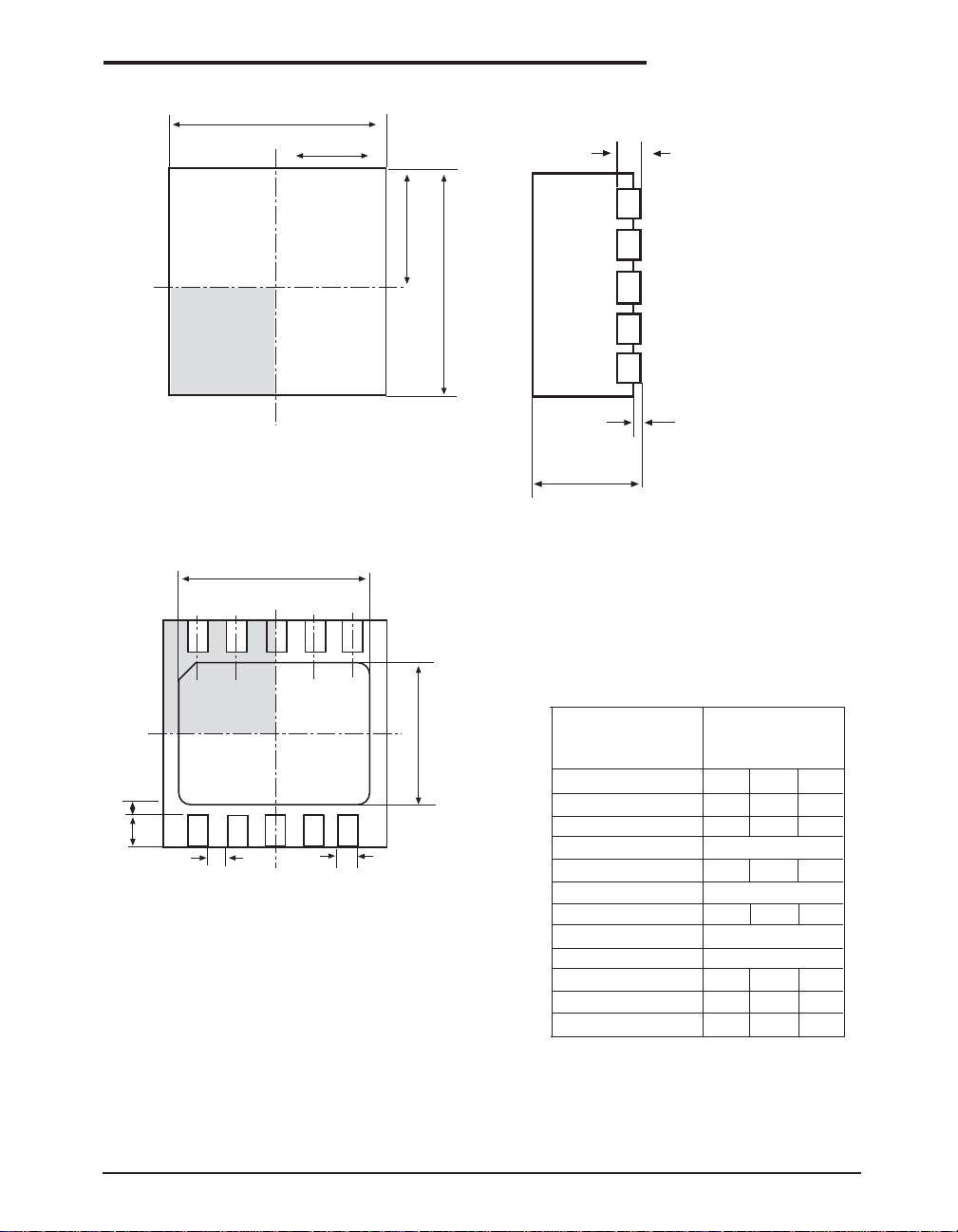
PACKAGE: 10 PIN DFN
D
1
Top View
D2
2
D/2
A3
E/2
E
A1
A
Side View
E2
10 Pin DFN
(JEDEC MO-229,
VEED-5 VARIATION)
DIMENSIONS
in
(mm)
SYMBOL MIN NOM MAX
K
L
e
b
A
A1
A3
b
D
D2
Bottom View
e
E
E2
K
L
Date: 08/24/04 SP6683 1.5X Charge Pump LED Driver for Parallel Configuration © Copyright 2004 Sipex Corporation
0.80 0.90 1.00
0.02 0.05
0
0.20 REF
0.18
0.25 0.30
3.00 BSC
2.20
0.50
PITCH
2.70
3.00 BSC
1.40
-
1.75
0.20
-
-
0.30 0.40 0.50
9
Page 10

ORDERING INFORMATION
Part Number Operating Temperature Range Package Type
SP6683ER .................................................. -40°C to +85°C ........................................................... 10 Pin DFN
SP6683ER/TR ............................................ -40°C to +85°C ........................................................... 10 Pin DFN
SP6683-03ER............................................. -40°C to +85°C ........................................................... 10 Pin DFN
SP6683-03ER/TR....................................... -40°C to +85°C ........................................................... 10 Pin DFN
*Contact factory for availability of the following parts
SP6683LVER.............................................. -40°C to +85°C ........................................................... 10 Pin DFN
SP6683LVER/TR........................................ -40°C to +85°C ........................................................... 10 Pin DFN
Available in lead free packaging. To order add "-L" suffix to part number.
Example: SP6683ER/TR = standard; SP6683ER-L/TR = lead free
/TR = Tape and Reel
Pack quantity is 3000 for DFN.
Corporation
ANALOG EXCELLENCE
Sipex Corporation
Headquarters and
Sales Office
233 South Hillview Drive
Milpitas, CA 95035
TEL: (408) 934-7500
FAX: (408) 935-7600
Sipex Corporation reserves the right to make changes to any products described herein. Sipex does not assume any liability arising out of the
application or use of any product or circuit described herein; neither does it convey any license under its patent rights nor the rights of others.
Date: 08/24/04 SP6683 1.5X Charge Pump LED Driver for Parallel Configuration © Copyright 2004 Sipex Corporation
10
 Loading...