

Page 1
®
3
T
SP6120
Low V oltage, AnyFETTM, Synchronous,Buck Controller
Ideal for 2A to 10A, High Performance, DC-DC Power Converters
FEATURES
■ Optimized for Single Supply, 3V - 5.5V Applications
■ High Efficiency: Greater Than 95% Possible
■ "AnyFET
PFET Or NFET High Side Switch
■ Selectable Discontinuous or Continuous Conduction
Mode For Use In Battery Or Bus Applications
■ Fast Transient Response
■ 16-Pin TSSOP, Small Size
■ Accurate 1% Reference Over Line, Load and Temperature
■ Accurate 10% Frequency
■ Accurate, Rail to Rail, 43mV, Over-Current Sensing
■ Resistor Programmable Frequency
■ Resistor Programmable Output Voltage
■ Capacitor Programmable Soft Start
■ Low Quiescent Current: 950µA, 10µA in Shutdown
■ Hiccup Over-Current Protection
TM"
Technology: Capable Of Switching Either
N/C
ENABLE
ISP
ISN
V
COMP
SS
R
OSC
1
2
3
4
5
FB
SP6120
16 Pin TSSOP
6
7
8
16
BST
15
GH
14
SWN
13
GND
12
PGND
11
GL
10
V
CC
9
PROG
Now Available in Lead Free Packaging
APPLICATIONS
■ DSP
■ Microprocessor Core
■ I/O & Logic
■ Industrial Control
■ Distributed Power
■ Low Voltage Power
DESCRIPTION
The SP6120 is a fixed frequency, voltage mode, synchronous PWM controller designed to work
from a single 5V or 3.3V input supply. Sipex's unique "AnyFET
TM"
Technology allows the SP6120
to be used for resolving a multitude of price/performance trade-offs. It is separated from the PWM
controller market by being the first controller to offer precision, speed, flexibility, protection and
efficiency over a wide range of operating conditions.
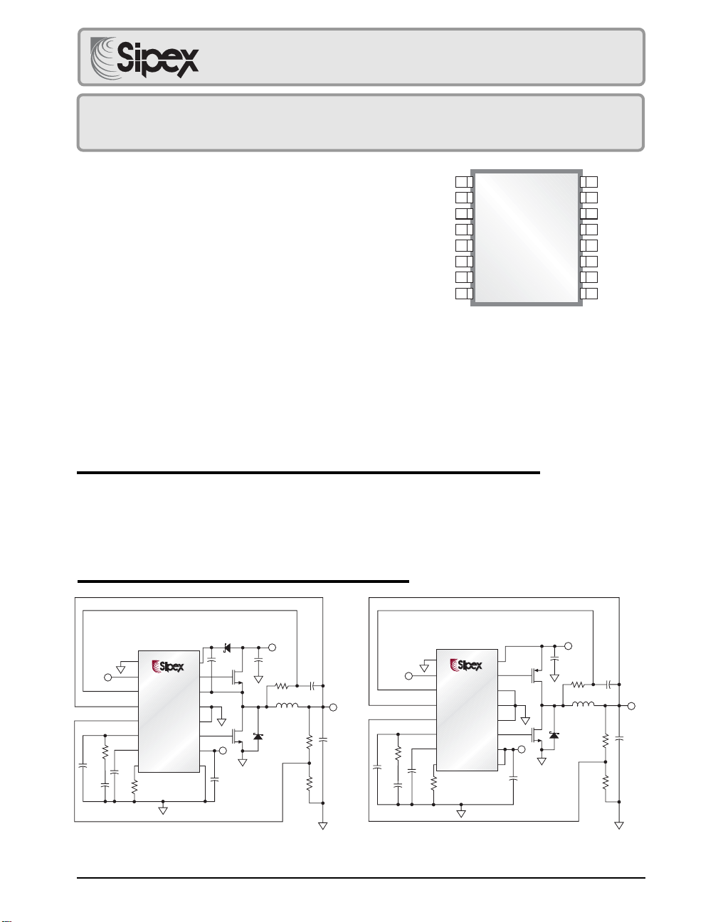
TYPICAL APPLICATIONS CIRCUIT
NMOS High Side Drive
PROG = GND
NC
ENABLE
CP
100pF
4.7nF
RZ
15k
CZ
C
0.33µF
ENABLE
ISP
SP6120
ISN
V
FB
COMP
SS
SS
R
OSC
R
OSC
18.7k
QT, QB = FAIRCHILD FDS6690A
®
®
PGND
PROG
MBR0530
C
BST
BST
1µF
GH
SWN
GND
GL
V
CC
CV
2.2µF
3.3V
C
IN
330µF x 2
QT
QB
DS
V
IN
CC
QT1 = FAIRCHILD FDS6375 (PMOS only)
L1 = PANASONIC ETQP6F2R5SFA
V
IN
4.7nF
CP
100pF
ENABLE
CZ
CS
RS
22.1k
L1
2.5µH
1.9V
39nF
1A to 8A
V
OUT
C
OUT
RF
470µF x
5.23k
RI
10k
DS = STMICROELECTRONICS STPS2L25U
= SANYO 6TPB330M
C
IN
C
OUT
PMOS High Side Drive
PROG = V
CC
®
FB
OSC
OSC
SP6120
®
PGND
PROG
BST
GH
SWN
GND
GL
V
CC
NC
ENABLE
ISP
ISN
V
COMP
SS
RZ
15k
R
C
SS
0.33µF
R
18.7k
= SANYO 4TPB470M
CV
2.2µF
3.3V
V
IN
C
IN
330µF x 2
QT1
QB
DS
V
IN
CC
CS
RS
22.1k
L1
2.5µH
1.9V
39nF
1A to 8A
C
OUT
RF
470µF x 3
5.23k
RI
10k
Date: 1/19/05 SP6120 Low Voltage, AnyFETTM, Synchronous, Buck Controller © Copyright 2005 Sipex Corporation
1
V
OU
Page 2

These are stress ratings only and functional operation
of the device at these ratings or any other above those
indicated in the operation sections of the specifications
below is not implied. Exposure to absolute maximum
rating conditions for extended periods of time may
affect reliability.
VCC.................................................................................... 7V
BST ............................................................................. 13.2V
BST-SWN......................................................................... 7V
SWN.......................................................................-1V to 7V
GH.......................................................... -0.3V to BST +0.3V
GH-SWN .......................................................................... 7V
All Other Pins ...........................................-0.3V to V
+0.3V
CC
ABSOLUTE MAXIMUM RATINGS
Peak Output Current < 10µs
GH, GL ............................................................................. 2A
Operating Temperature Range
SP6120C ................................................ 0°C to +70°C
SP6120E..............................................-40°C to +85 °C
Junction Temperature, T
Storage Temperature Range ....................... -65˚C to +150˚C
Power Dissipation
ESD Rating ............................................................ 2kV HBM
..........................................+125°C
J
Unless otherwise specified: 3.0V < VCC <5.5V, 3.0V < BST < 13.2, R
CGH = CGL = 3.3nF, V
= 1.25V, ISP = ISN = 1.25V, SWN = GND = PGND = 0V, -40°C < T
FB
RETEMARAPSNOITIDNOCNIMPYTXAM
TNERRUCTNECSEIUQ
V
CC
V
CC
tnerruCylppuSgnihctiwSoN-59.08.1Am
)delbasiD(tnerruCylppuSV0=ELBANE-502
tnerruCylppuSTSBgnihctiwSoN-102
REIFILPMARORRE
ecnatcudnocsnarTreifilpmArorrE 006
tnerruCkniSPMOCV
tnerruCecruoSPMOCV
BF
stluaF
BF
ecnedepmItuptuOPMOC 3
V
BF
tnerruCsaiBtupnI -06001
ECNEREFER
ecnerefeRreifilpmArorrEytinUnipmArorrEhtiwdemmirT
niaG
V
BF
V
BF
rotarapmoCwoL%3 |3-|
rotarapmoChgiH%3 3
HTAPYALED&ROTALLICSO
ELECTRICAL CHARACTERISTICS
= 18.7kΩ, C
OSC
oN,V5.0=PMOC,V53.1=
V6.1=PMOC,V51.1=515356
= 0.1µF, CSS = 0.1µF, ENABLE = 3V,
COMP
<85°C (Note 1)
AMB
515356
832.1052.1262.1V
STINU
µA
µA
µS
µA
µA
mhOM
An
FERV%
FERV%
ycneuqerFrotallicsO 072003033
oitaRytuDCD%001-lortnoCnIpooL
R
egatloVhtiwsevoM-ylnOnoitamrofnI
CSO
2#ycneuqerFrotallicsOR
CSO
mhOk2.01=054005055
elbissop
mirTrotallicsO
htdiWesluPHGmuminiMV
CC
PMOCpupmaR,V5.4>
stratsHGlitnuV6.0>egatloV
59%
56.0V
021sn
zHk
zHk
gnihctiwS
Date: 1/19/05 SP6120 Low Voltage, AnyFETTM, Synchronous, Buck Controller © Copyright 2005 Sipex Corporation
2
Page 3

Unless otherwise specified: 3.0V < VCC <5.5V, 3.0V < BST < 13.2, R
CGH = CGL = 3.3nF, V
= 1.25V, ISP = ISN = 1.25V, SWN = GND = PGND = 0V, -40°C < T
FB
RETEMARAPSNOITIDNOCNIMPYTXAM
TRATSTFOS
tnerruCegrahCSSV
tnerruCegrahcsiDSSV
tnerruCegrahcsiDPMOCV
egatloVpmalCPMOCV
V5.1=520507
SS
V5.1=257
SS
PMOC
V,V0.1<
BF
V5.2=1.24.28.2
SS
dlohserhTkOSS 8.10.22.2
teseRtluaFSS 2.052.03.0
egatloVpmalCSS 1.24.28.2
SROTARAPMOCTNERRUCOREZ&TNERRUCREVO
ELECTRICAL CHARACTERISTICS
= 18.7kΩ, C
OSC
detaitinItluaF,V5.0=002005-
= 0.1µF, CSS = 0.1µF, ENABLE = 3V,
COMP
<85°C (Note 1)
AMB
STINU
µA
µA
µA
V
V
V
V
egatloV
dlohserhTrotarapmoCtnerruCrevO
tupnIedoMnommoCliaRotliaR
233445Vm
tnerruCsaiBtupnIPSI,NSI -06052
dlohserhTrotarapmoCtnerruCoreZNSIV-PSIV2
OLVU/ELBANE
V
CC
V
CC
V
CC
dlohserhTtratS 57.258.259.2
dlohserhTpotS 56.257.29.2
siseretsyH
dlohserhTelbanE 56.0
tnerruCecruoSniPelbanE
6.049
001Vm
1.1
REVIRDETAG
emiTesiRHGV
emiTllaFHGV
emiTesiRLGV
emiTllaFLGV
emiTpalrevO-noNLGotHGV
emiTpalrevO-noNHGotLGV
Note 1: Specifications to -40°C are guaranteed by design, characterization and correlation with statistical process control.
V5.4>
CC
V5.4>
CC
V5.4>
CC
V5.4>
CC
V5.4>
CC
V5.4>
CC
-04011sn
-04011sn
-04011sn
-04011sn
06sn
06sn
An
Vm
V
V
54.1
V
µA
Date: 1/19/05 SP6120 Low Voltage, AnyFETTM, Synchronous, Buck Controller © Copyright 2005 Sipex Corporation
3
Page 4

PIN DESCRIPTION
EMANNOITCNUF
C/NnoitcennoCoN 1
NIP
REBMUNREBMUN
REBMUNREBMUN
REBMUN
0216PS
ELBANE
PSI
NSI
.noitceteD
.trapselbasidV56.0<elbaneV,trapehtelbanelliw
.emitesnopser)pyt(sµ01htiwdlohserhtVm34
tnerruC-revOroftupniliaRotliaR:tupnIevitageNesneStnerruC
V5.1>elbaneVrognitaolF.pullupAu4lanretnihtiwtupnielbitapmocLTT
2
,noitceteDtnerruC-revOroftupnIliaRotliaR:tupnIevitisoPesneStnerruC
3
4
sasevresdnareifilpmarorreehtfotupnignitrevnI:niPegatloVkcabdeeF
V
BF
tuptuoehT.retrevnockcubehtroftniopkcabdeefegatlovtuptuoeht
5
.redividrotsiserlanretxenahguorhtdetsujdaebnacdnadesnessiegatlov
yllacipytsikrowtengaldaelA:niPnoitasnepmoCreifilpmArorrE
PMOC
sinipsihT.poolkcabdeefehtetasnepmocotnipsihtotdetcennoc
6
.mumixamV8.2otdetimilsidnaegatlovSSehtybdepmalc
Fµ10.0A.pu-tratsnoAµ05secruosnipsihT:niPgnimmargorPtratStfoS
atratstfosotecnaticapachguoneyllacipytsinipsihtnoroticapacFµ1ot
SS
nipsihtybdellortnocsignimitedompuccih,noitiddanI.ylppusrewop
7
V7.2otdepmalcsiegatlovSSehT.tnerrucegrahcsidAµ5ehthguorht
.mumixam
R
CSO
margorpotdesusidnuorgotrotsiserA:niPgnimmargorPycneuqerF
8
.zHk005,smhO002,01;zHk003,smhO007,81-seulavlacipyT.ycneuqerf
:niPgnimmargorP
SUONITNOC/TEFN=EDOM;DNG=GORP
GORP
V
CC
k86=GORP Ω SUONITNOCSID/TEFN=EDOM;DNGot
V=GORP
CC
k86=GORP Ω Vot
CC
SUONITNOC/TEFP=EDOM;
SUONITNOCSID/TEFP=EDOM;
ssapybylreporP.nipsihtotdekoohoslaserutcurtsDSE:niPylppuS.C.I
.roticapaccimarecRSE/LSEwolahtiwDNGPotnipsiht
9
01
LG.ytilibapacevirdlacipytsn02/Fn1:revirDTEFsuonorhcnyS 11
DNGP
.ecnamrofreplamitporofsnip.C.I
taDNGotyltceriDtcennoC.egatSrewoProfdesU:niPdnuorGrewoP
21
DNG.C.IrofnipdnuorgniaM:niPdnuorG 31
NWS
.snoitacilppaegatlovwolrofDNGotdeit
eboslanaC.ecnereferrevirdTEFSOMedishgiH:ecnerefeRedoNhctiwS
41
margorPnognidnepedTEFProTEFNebnaC:revirDTEFSOMediShgIH
HG
signitaregatlovmumixaM.ytilibapacevirdlacipytsn02/Fn1.edoM
51
.NWSotdecnerefer
TSB.niPylppuSrevirDediShgiH 61
Date: 1/19/05 SP6120 Low Voltage, AnyFETTM, Synchronous, Buck Controller © Copyright 2005 Sipex Corporation
4
Page 5
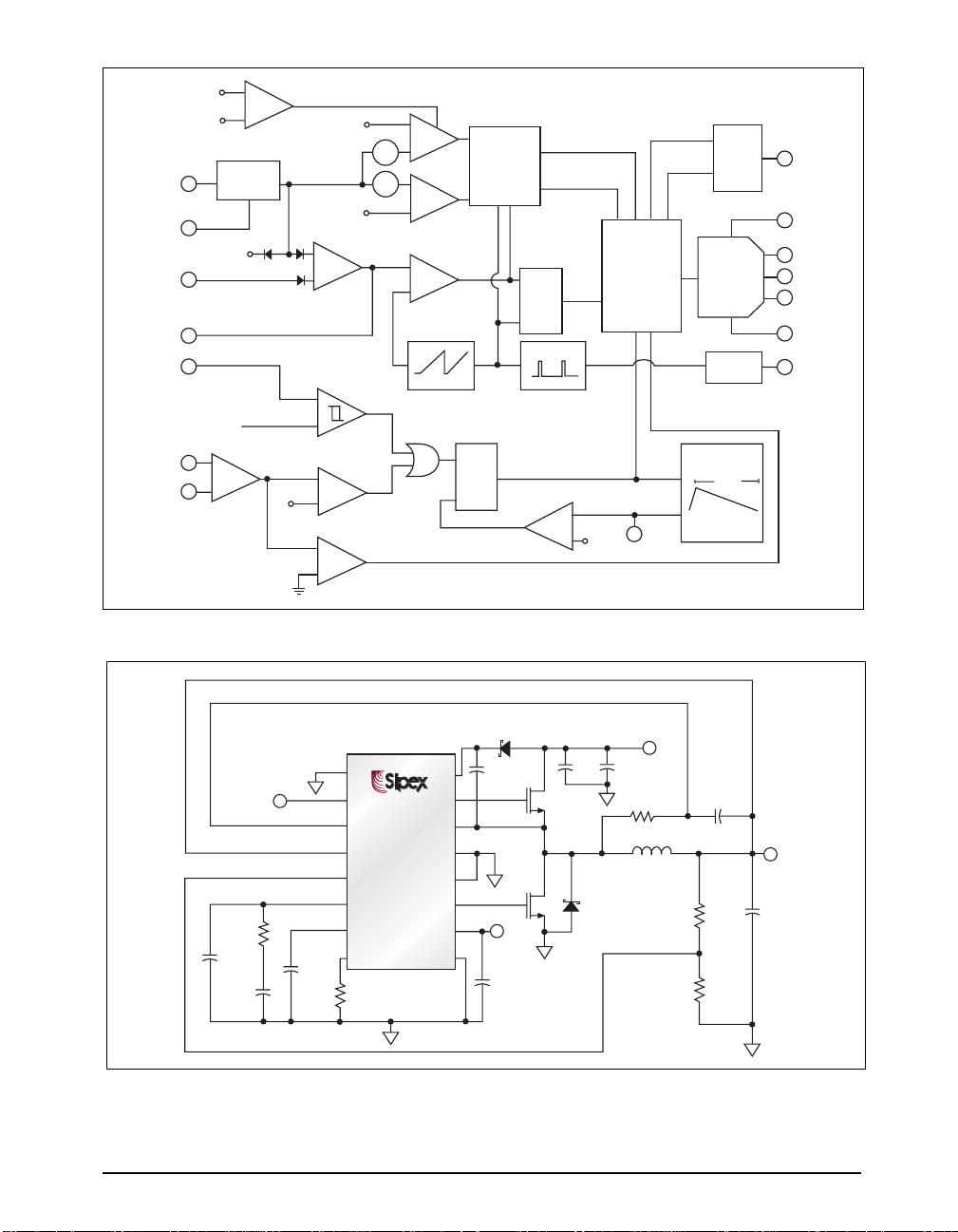
BLOCK DIAGRAM
3
SS
+
-
2V
Reference
2
ENABLE
GND
13
SS
V
5
FB
COMP
6
V
10
CC
2.85 V
2.75 V
ISP
3
+
ISN
x 10
4
-
ON
OFF
430mV
1.25V
V
FB
V
FB
V
FB
GM
Error Amplifier
+
-
UVLO
-
+
OVC
+
10µs
-
-
+
3% Low ENABLE
-
3%
+ -
+
3%
- +
-
+
-
+
1V RAMP
Zero crossing detect
Window
Comparator
Logic
F (kHz) = 5.7E6/R
Set Dominant
Fault Latch
S
Q
R
RESET
Dominant
PWM Latch
R
FAULT
Continuous/
(Ω)
Discontinuous
NFET/PFET
Driver
Logic
I
CHARGE
& Hiccup Logic
Program
Logic
Synchronous
Driver
0.65V
Soft Start
T
OFF
9
PROG
BST
16
15
GH
SWN
14
11
GL
12
PGND
8
R
OSC
ON 100%
OFF 100%
QPWM
Q
S
OSC
-
250mV
7
SS
+
APPLICATION SCHEMATIC
NMOS High Side Drive
PROG = GND
®
®
SP6120
PGND
PROG
CP
100pF
ENABLE
CZ
4.7nF
NC
ENABLE
ISP
ISN
V
FB
COMP
RZ
15k
C
SS
0.33µF
SS
R
R
18.7k
OSC
OSC
Figure 1. Schematic 3.3V to 1.9V Power Supply
QT, QB = FAIRCHILD FDS6690A
L1 = PANASONIC ETQP6F2R5SFA
DS = STMICROELECTRONICS STPS2L25U
Date: 1/19/05 SP6120 Low Voltage, AnyFETTM, Synchronous, Buck Controller © Copyright 2005 Sipex Corporation
SWN
GND
BST
V
MBR0530
C
C
BST
1µF
GH
GL
V
CV
2.2µF
IN
CC
CC
B
1µF
QT
QB
DS
C
330µF x 2
3.3V
V
IN
IN
5.23k
CS
1.9V
39nF
1A to 8A
V
OUT
C
RF
RI
10k
OUT
470µF x
22.1k
RS
L1
2.5µH
CIN = SANYO 6TPB330M
= SANYO 4TPB470M
C
OUT
5
Page 6
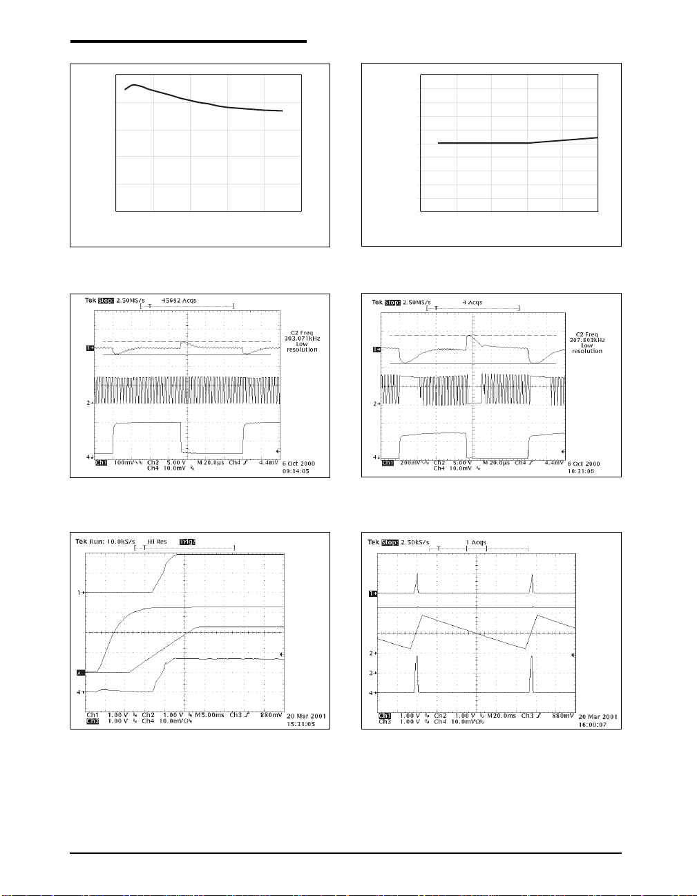
Refer to circuit in Figure 1 with VIN = 3.3V; V
100
90
80
70
Efficiency (%)
60
50
0246
Output Current (A)
Figure 2. Efficiency vs. Output Current Figure 3. Load Regulation
Gate High
(1A/div)
I
OUT
= 1.9V, R
OUT
= 18.7kΩ, and T
OSC
= +25°C unless otherwise noted.
AMB
1.925
1.920
1.915
1.910
1.905
(V)
1.900
OUT
1.895
V
1.890
1.885
1.880
810
V
OUT
1.875
012345
Gate High
I
(5A/div)
OUT
TYPICAL PERFORMANCE CHARACTERISTICS
Load Current (A)
V
OUT
Figure 4. Load Step Response: 0.4A to 2A
V
OUT
V
IN
Soft Start
(1A/div)
I
IN
Figure 6. Start-Up Response: 5A Load
Figure 5. Load Step Response: 0.4A to 7A
V
OUT
V
IN
Soft Start
I
(5A/div)
OUT
Figure 7. Overcurrent: 9A Load
Date: 1/19/05 SP6120 Low Voltage, AnyFETTM, Synchronous, Buck Controller © Copyright 2005 Sipex Corporation
6
Page 7
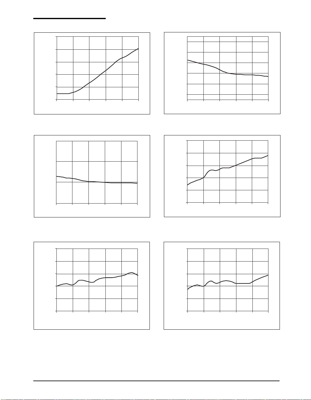
Unless otherwise specified: VCC = BST = ENABLE = 3.3V, R
ISP = ISN = 1.25V, SWN = GND = PGND = 0V, T
0.30
0.20
0.10
(%)
REF
0.00
1.25V
-0.10
-0.20
-40 -15 10 35 60 85
Temperature (°C)
AMB
Figure 8. Error Amplifier Reference vs. Temperature Figure 9. Overcurrent Comparator Threshold Voltage
= 25°C.
= 18.7kΩ, C
OSC
= 0.1µF, CSS = 0.1µF, CGH = CGL = 3.3nF, VFB = 1.25V,
COMP
48
46
44
42
40
38
-40 -15 10 35 60 85
Overcurrent (mV)
Temperature (°C)
vs. Temperature
TYPICAL PERFORMANCE CHARACTERISTICS: Continued
-44
-45
-46
SS Charge (µA)
-47
-40 -15 10 35 60 85
Temperature (°C)
Figure 10. SS Charge Current vs. Temperature with
VSS = 1.5V
3.6
3.4
)
REF
3.2
High (% V
3.0
FB
V
2.8
2.6
-40 -15 10 35 60 85
Temperature (°C)
5.25
5.20
5.15
5.10
SS Discharge (µA)
5.05
5.00
-40 -15 10 35 60 85
Temperature (°C)
Figure 11. SS Discharge Current vs. Temperature with
VSS = 1.5V
-2.2
-2.4
)
REF
-2.6
Low (% V
-2.8
FB
V
-3.0
-3.2
-40 -15 10 35 60 85
Temperature (°C)
Figure 12. VFB 3% High Comparator vs. Temperature Figure 13. VFB 3% Low Comparator vs. Temperature
Date: 1/19/05 SP6120 Low Voltage, AnyFETTM, Synchronous, Buck Controller © Copyright 2005 Sipex Corporation
7
Page 8
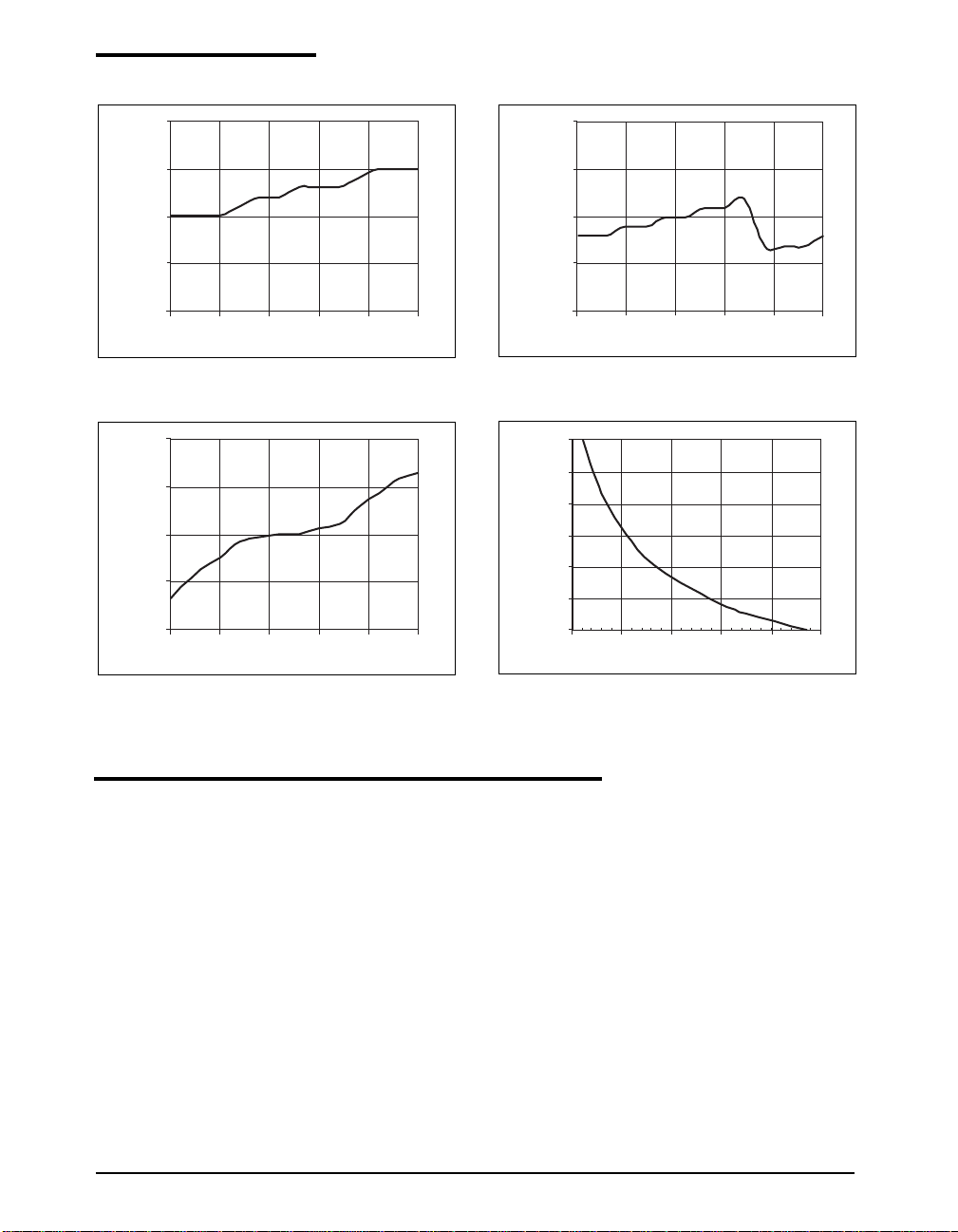
Unless otherwise specified: VCC = BST = ENABLE = 3.3V, R
TYPICAL PERFORMANCE CHARACTERISTICS: Continued
ISP = ISN = 1.25V, SWN = GND = PGND = 0V, T
AMB
= 25°C.
= 18.7k, C
OSC
= 0.1µF, CSS = 0.1µF, CGH = CGL = 3.3nF, VFB = 1.25V,
COMP
2.900
2.875
2.850
Start (V)
CC
V
2.825
2.800
-40 -15 10 35 60 85
Temperature (°C)
2.850
2.825
2.800
Stop (V)
CC
V
2.775
2.750
-40 -15 10 35 60 85
Temperature (°C)
Figure 14. VCC Start Threshold vs. Temperature Figure 15. VCC Stop Threshold vs. Temperature
302
301
300
Frequency (kHz)
299
298
-40 -15 10 35 60 85
Temperature (°C)
Figure 16. Oscillator Frequency vs. Temperature
800
700
600
500
400
Frequency (kHz)
300
200
51015202530
R
(kΩ)
OSC
Figure 17. Oscillator Frequency vs. R
and CGH = CGL = Open.
with VCC = 5V
OSC
THEORY OF OPERATIONS
General Overview
The SP6120 is a constant frequency, voltage
mode PWM controller for low voltage, DC/DC
step down converters. It has a main loop where
an external resistor (R
) sets the frequency
OSC
and the driver is controlled by the comparison of
an error amp output (COMP) and a 1V ramp
signal. The error amp has a transconductance of
600µS, an output impedance of 3 MΩ, an internal pole at 2 MHz and a 1.25V reference input.
Although the main control loop is capable of 0%
and 100% duty cycle, its response time is limited by the external component selection. Therefore, a secondary loop, including a window
Date: 1/19/05 SP6120 Low Voltage, AnyFETTM, Synchronous, Buck Controller © Copyright 2005 Sipex Corporation
comparator positioned 3% above and below the
reference, has been added to insure fast response to line and load transients. A unique
“Ripple & Frequency Independent” algorithm,
added to the secondary loop, insures that the
window comparator does not interfere with the
main loop during normal operation. In addition
to receiving driver commands from the main
and secondary loops, the Driver Logic is also
controlled by the Programming Logic, Fault
Logic and Zero Crossing Comparator. The Programming Logic tells the Driver Logic whether
the controller is using a PFET or NFET high side
8
Page 9

THEORY OF OPERATIONS: Continued
driver as well as whether the controller is operating in continuous or discontinuous mode. The
Fault Logic holds the high and low side drivers
off if VCC dips below 2.75V, if an over current
condition exists, or if the part is disabled through
the ENABLE pin. The Zero Crossing Comparator turns the lower driver off if the conduction
current reaches zero and the Driver Logic has
made an attempt to turn the lower driver on and
the Programming Logic is set for discontinuous
mode. Lastly, the 4Ω drivers have internal gate
non-overlap circuitry and are designed to drive
MOSFETs associated with converter designs in
the 5A to 10A range. Typically the high side
driver is referenced to the SWN pin; further
improving the efficiency and performance of
the converter.
ENABLE
Low quiescent mode or “Sleep Mode” is initiated by pulling the ENABLE pin below 650mV.
The ENABLE pin has an internal 4µA pull-up
current and does not require any external interface for normal operation. If the ENABLE pin
is driven from a voltage source, the voltage must
be above 1.45V in order to guarantee proper
“awake” operation. Assuming that VCC is above
2.85V, the SP6120 transitions from “Sleep
Mode” to “Awake Mode” in about 20µs to 30µs
and from “Awake Mode” to “Sleep Mode” in a
few microseconds. SP6120 quiescent current in
sleep mode is 20µA maximum. During Sleep
Mode, the high side and low side MOSFETs are
turned off and the COMP and SS pins are held
low.
UVLO
Assuming that the ENABLE pin is either pulled
high or floating, the voltage on the VCC pin then
determines operation of the SP6120. As V
CC
rises, the UVLO block monitors VCC and keeps
the high side and low side MOSFETs off and the
COMP and SS pins low until VCC reaches 2.85V.
If no faults are present, the SP6120 will initiate
a soft start when VCC exceeds 2.85V. Hysteresis
(about 100mV) in the UVLO comparator provides noise immunity at start-up.
Soft Start
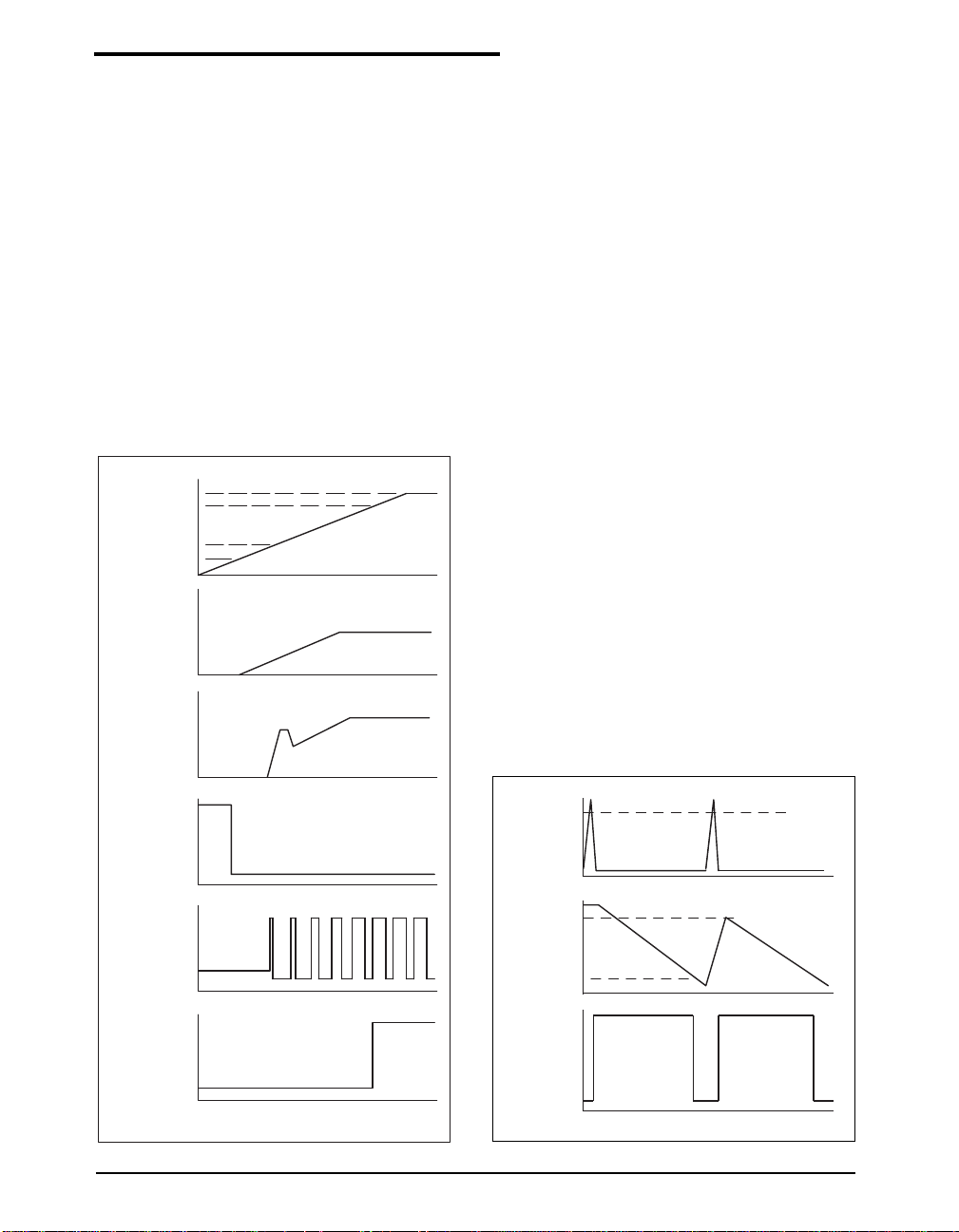
(see figures on next page)
Soft start is required on step-down controllers to
prevent excess inrush current through the power
train during start-up. Typically this is managed
by sourcing a controlled current into a programming capacitor (on the SS pin) and then using
the voltage across this capacitor to slowly ramp
up either the error amp reference or the error
amp output (COMP). The control loop creates
narrow width driver pulses while the output
voltage is low and allows these pulses to increase to their steady-state duty cycle as the
output voltage increases to its regulated value.
As a result of controlling the inductor
volt*second product during start-up, inrush current is also controlled.
The presence of the output capacitor creates
extra current draw during start-up. Simply stated,
dV
/dt requires an average sustained current
OUT
in the output capacitor and this current must be
considered while calculating peak inrush current and over current thresholds. Since the
SP6120
Soft Start: (continued)
ramps up the error amp reference voltage, an
expression for the output capacitor current can
be written as:
IC
OUT
= (C
OUT/CSS
) * (V
/1.25) * 50µA
OUT
As the figure shows, the SS voltage controls a
variety of signals. First, provided all the external fault conditions are removed, the fault latch
is reset and the SS cap begins to charge. When
the SS voltage reaches around 0.3V, the error
amp reference begins to track the SS voltage
while maintaining the 0.3V differential. As the
SS voltage reaches 0.7V, the driver begins to
switch the high side and low side MOSFETs
with narrow pulses in an effort to keep the
converter output regulated. As the error amp
reference ramps upward, the driver pulses widen
until a steady state value is reached. The “bump”
in the inductor current transfer curve is indicative of excess charge current incurred due to the
Date: 1/19/05 SP6120 Low Voltage, AnyFETTM, Synchronous, Buck Controller © Copyright 2005 Sipex Corporation
9
Page 10
THEORY OF OPERATIONS: Continued
finite propagation delay of the controller. When
the SS voltage reaches 2.0V, the secondary loop
including the 3% window comparator is enabled. Lastly, the SS voltage is clamped at 2.4V,
ending the soft start charge cycle.
Hiccup Mode
When the converter enters a fault mode, the
driver holds the high side and low side MOSFETs
off for a finite period of time. Provided the part
is enabled, this time is set by the discharge of the
SS capacitor. The discharge time is roughly 10
times the charge interval thereby giving the
power supply plenty of time to cool during an
over current fault. The driver off-time is predominantly determined by the discharge time.
2.4V
SS Voltage
Error Amplifier
Reference
Voltage
Inductor Current
FAULT
Reset Voltage
2.0V
0.7V
0.25V
1.25V
I
LOAD
V(VCC)
dV
/dt = 50µA/C
SS
0V
= V(Eamp REF)* (1+RF/RI)
V
OUT
0V
0V
SS
Restart will occur just like a normal soft start
cycle.
However, if a fault occurs during the soft start
charge cycle, the FAULT latch is immediately
set, turning off the high side and low side
MOSFETs. The MOSFETs remain off during
the remainder of the charge cycle and subsequent discharge cycle of the SS capacitor. Again,
provided there are no external fault conditions,
the FAULT latch will be reset when the SS
voltage reaches 250 mV.
Over Current Protection
The SP6120 over current protection scheme is
designed to take advantage of three popular
detection schemes: Sense Resistor, Trace Resistor or Inductor Sense. Because the detection
threshold is only 43mV, both trace resistor and
inductor sense become attractive protection
schemes. The inductor sense scheme adds no
additional dc loss to the converter and is an
excellent alternative to Rdson based schemes;
providing continuous current sensing and flexible MOSFET selection. An internal, 10µs filter
conditions the over current signal from transients generated during load steps. In addition,
because the over current inputs, ISP and ISN,
are capable of rail to rail operation, the SP6120
provides excellent over current protection during conditions where VIN approaches V
43mV
V(ISP) - V(ISN)
OUT
.
2.4V
2.0V
250mV
V(VCC)
0V
0V
0V
0V
V(VCC)
SWN
Voltage
0V
V(VCC)
3% Low
Enable Voltage
0V
Date: 1/19/05 SP6120 Low Voltage, AnyFETTM, Synchronous, Buck Controller © Copyright 2005 Sipex Corporation
TIME
SS Voltage
FAULT V oltage
10
Page 11
Zero Crossing Detection
In some applications, it may be undesirable to have
negative conduction current in the inductor. This
situation happens when the ripple current in the
inductor is higher than the load current. Therefore,
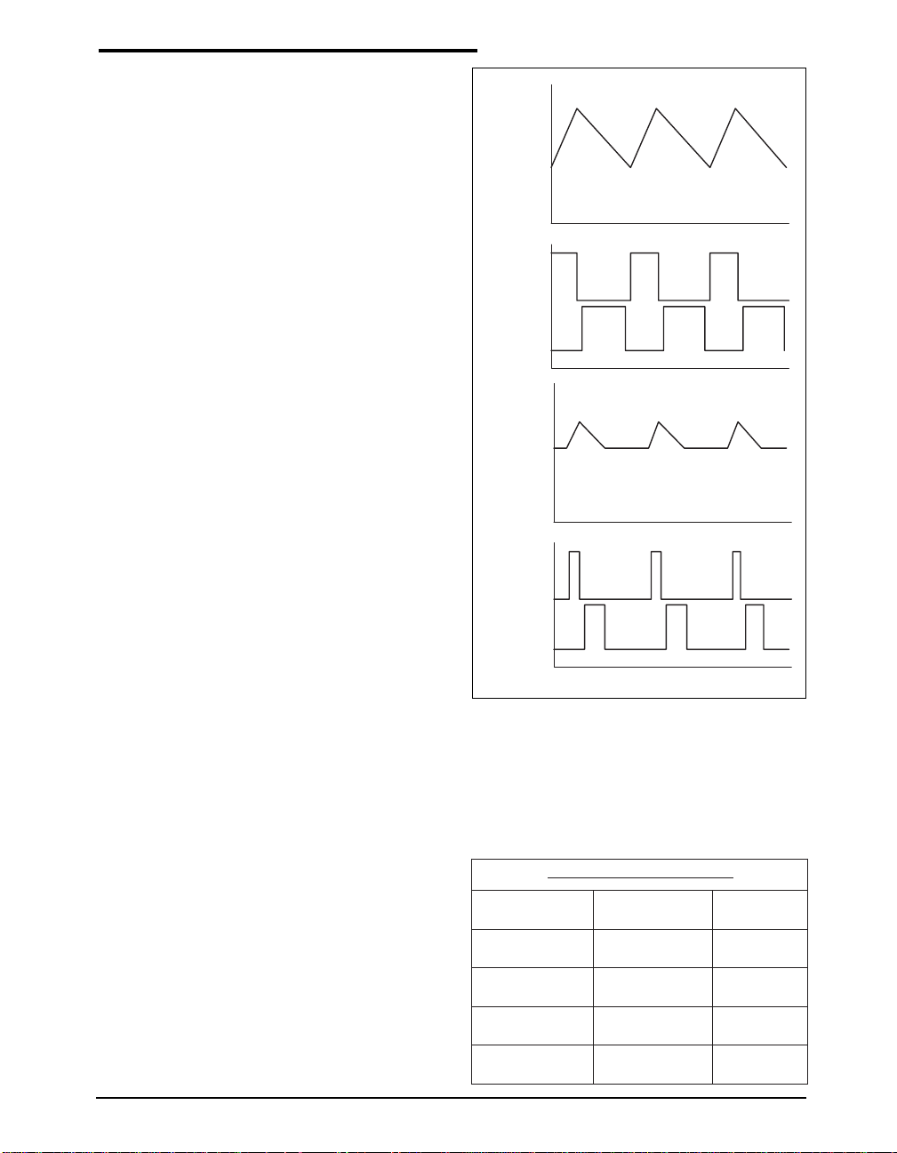
the SP6120 provides an option for “discontinuous” operation. If the Program Logic (see next
section) is set for discontinuous mode, then the
Driver Logic looks at the Zero Crossing Comparator and the state of the lower gate driver. If the low
side MOSFET was “on” and V(ISP)-V(ISN) < 0
then the low side MOSFET is immediately turned
off and held off until the high side MOSFET is
turned “on”. When the high side MOSFET turns
“on” , the Driver Logic is reset. The following
figures show continuous and discontinuous operation for a converter with an NFET high side
MOSFET.
Discontinuous vs. Continuous Mode
The discontinuous mode is used when better light
load efficiency is desired, for example in portable
applications. Additionally, for power supply sequencing in some applications the DC-DC converter output is pre-charged to a voltage through a
switch at start-up, and discontinuous operation
would be required to prevent reverse inductor
current from discharging the pre-charge voltage.
The continuous mode is preferable for lower noise
and EMI applications since the discontinuous mode
can cause ringing of the switch node voltage when
it turns both switches off. Another example where
continuous mode could be required is one where
the inductor has an extra winding used for an overwinding regulator and thus continuous conduction
is necessary to produce this second output voltage.
Program Logic
The Program pin (PROG) of the SP6120 adds a
new level of flexibility to the design of DC/DC
converters. A 10µA current flows either into or out
of the Program pin depending on the initial potential presented to the pin. If no resistor is present, the
Program Logic simply looks at the potential on the
pin, sets the mode to “continuous” and programs
NFET or PFET high side drive accordingly. If the
68kΩ resistor is present,
THEORY OF OPERATIONS: Continued
Continuous
Load
Current
0A
GH, GL
Voltage
0V
0V
Discontinuous
Load
Current
0A
GH, GL
Voltage
0V
0V
TIME
Program Logic: continued
the voltage drop across the resistor signals the
SP6120 to put the Driver Logic in “discontinuous”
mode. With one pin and a 68kΩ resistor, the
SP6120 can be configured for a variety of operating modes:
ELBATHTURTCIGOLMARGORP
NIPMARGORPTEFPROTEFNEDOM
DNGottrohSTEFNsuounitnoC
k86 Ω DNGotTEFNsuounitnocsiD
k86 Ω Vot
VottrohS
CC
CC
TEFPsuounitnoC
TEFPsuonitnocsiD
Date: 1/19/05 SP6120 Low Voltage, AnyFETTM, Synchronous, Buck Controller © Copyright 2005 Sipex Corporation
11
Page 12
The NFET/PFET programmability is for the
high side MOSFET. When designing DC/DC
converters, it is not always obvious when to use
an NFET with a charge pump or a simple PFET
for the high side MOSFET. Often, the controller
has to be changed, making performance evaluations difficult. This difficulty is worsened by
the limited availability of true low voltage controllers. In addition, by also programming the
mode, continuous or discontinuous, switch mode
power designs that are successful in bus applications can now find homes in portable applications.
THEORY OF OPERATIONS: Continued
Secondary Loop (continued)
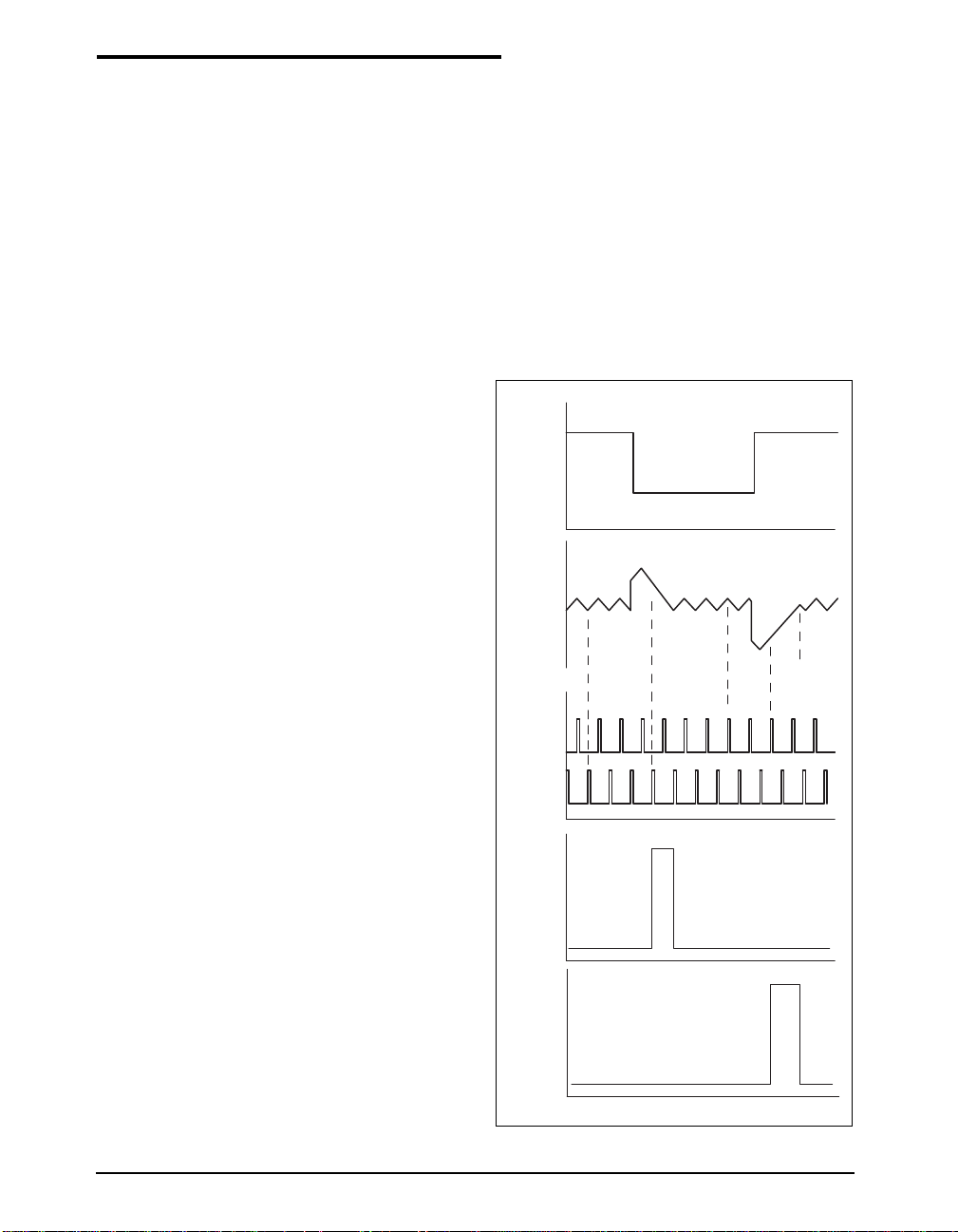
any additional loops, the current peak and valley are determined by the edges associated with
the on-time in the main loop. The set pulse
corresponding to the start of an on-time indicates a current valley and the reset pulse corresponding to the end of an on-time indicates a
current peak. In effect, the main loop determines the status of the secondary loop.
Notice that the output voltage appears to coast
toward the regulated value during periods where
the main loop would be telling the drivers to
Secondary Loop (3% Window Comparator)
DSP, microcontroller and microprocessor applications have very strict supply voltage requirements. In addition, the current requirements to these devices can change drastically.
Linear regulators, typically the workhorse for
DC/DC step-down, do a great job managing
accuracy and transient response at the expense
of efficiency. On the other hand, PWM switching regulators typically do a great job managing
efficiency at the expense of output ripple and
line/load step response. The trick in PWM
controller design is to emulate the transient
response of the linear regulator.
Of course improving transient response should
be transparent to the power supply designer.
Very often this is not the case. Usually the very
circuitry that improves the controllers transient
response adversely interferes with the main
PWM loop or complicates the board level design of the power converter.
The SP6120 handles line/load transient response
in a new way. First, a window comparator
detects whether the output voltage is above or
below the regulated value by 3%. Then, a
proprietary “Ripple & Frequency Independent”
algorithm synchronizes the output of the window comparator with the peak and valley of the
inductor current waveform. 3% low detection is
synchronized with inductor current peak; 3%
high detection is synchronized with the inductor
current valley. However, in order to eliminate
DC Load
Current
Output
Voltage
Main Loop
3% High
Latch On
3% Low
Latch On
Reset
V(V
V(V
MAX
MIN
V
0A
OUT
.
3% High Sync.
Set
)
CC
0V
)
CC
0V
3% High
TIME
3% Low
3% Low Sync.
1.25V Cross.
Date: 1/19/05 SP6120 Low Voltage, AnyFETTM, Synchronous, Buck Controller © Copyright 2005 Sipex Corporation
12
Page 13
THEORY OF OPERATIONS: Continued
switch. It is during this interval that the 3%
window comparator has taken control away from
the main loop. The main loop regains control
only if the output voltage crosses through its
regulated value. Also notice where the 3%
comparator takes over. The output voltage is
considered “high” only if the trough of the ripple
is above 3%. The output voltage is considered
“low” only if the peak of the ripple is below 3%.
By managing the secondary loop in this fashion,
the SP6120 can improve the transient response
of high performance power converters without
causing strange disturbances in low to moderate
performance systems.
Driver Logic
Signals from the PWM latch (QPWM), Fault
latch (FAULT), Program Logic, Zero Crossing
Comparator, and 3% Window Comparators all
flow into the Driver Logic. The following is a
truth table for determining the state of the GH
and GL voltages for given inputs:
ELBATHTURTCIGOLREVIRD
TLUAF1100000000
roMWPQ
XX11000000
PMOC%3
TEFP/TEFNNPNPNPNPNP
CSID/TNOCXXXXCCDDDD
SSORCOREZXXXXXX00 11
HG011001010 1
LG0000111100
The QPWM and 3% Comparators are grouped
together because 3% Low is the same as QPWM
= 1 and 3% High is the same as QPWM = 0.
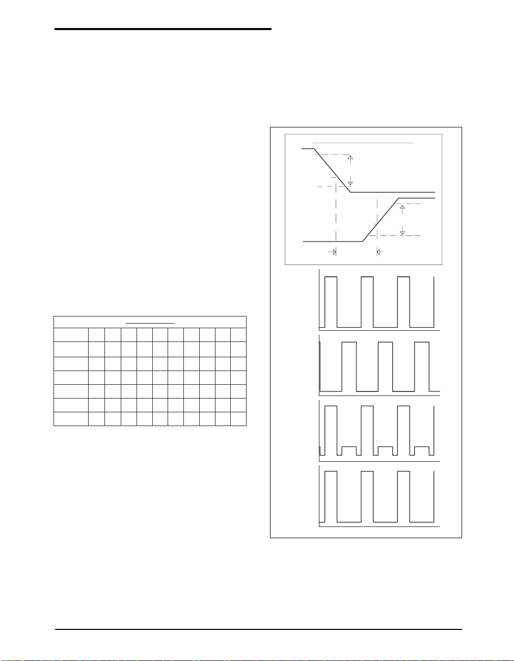
driver waveforms for the 5V, high side NFET
design.
As with all synchronous designs, care must be
taken to ensure that the MOSFETs are properly
chosen for non-overlap time, peak current capability and efficiency.
90%
V(BST)
V(V
= VIN)
10%
2V
0V
CC
)
0V
~0V
IN
)
GATE DRIVER TEST CONDITONS
FALL TIME
2V
NON-OVERLAP
90%
RISE TIME
10%
GH
Voltage
GL
Voltage
SWN
Voltage
5V
GH (GL)
5V
GH (GL)
V(V
CC
~V(Diode) V
~2V(V
BST
Output Drivers
Voltage
The driver stage consists of one high side, 4Ω
driver, GH and one low side, 4Ω, NFET driver,
GL. As previously stated, the high side driver
~V(V
IN
)
TIME
can be configured to drive a PFET or an NFET
high side switch. The high side driver can also be
configured as a switch node referenced driver.
Due to voltage constraints, this mode is mandatory for 5V, single supply, high side NFET
applications. The following figure shows typical
Date: 1/19/05 SP6120 Low Voltage, AnyFETTM, Synchronous, Buck Controller © Copyright 2005 Sipex Corporation
13
Page 14

APPLICATIONS INFORMATION
Inductor Selection
There are many factors to consider in selecting
the inductor including cost, efficiency, size and
EMI. In a typical SP6120 circuit, the inductor is
chosen primarily for value, saturation current
and DC resistance. Increasing the inductor value
will decrease output voltage ripple, but degrade
transient response. Low inductor values provide the smallest size, but cause large ripple
currents, poor efficiency and more output capacitance to smooth out the larger ripple current. The inductor must also be able to handle
the peak current at the switching frequency
without saturating, and the copper resistance in
the winding should be kept as low as possible to
minimize resistive power loss. A good compromise between size, loss and cost is to set the
inductor ripple current to be within 20% to 40%
of the maximum output current.
The switching frequency and the inductor operating point determine the inductor value as
follows:
L−=
(max)
OUTINOUT
IKFV
(max)(max)
OUTrSIN
)(
VVV
where:
FS = switching frequency
Kr = ratio of the ac inductor ripple current to
the maximum output current
The peak to peak inductor ripple current is:
)( −
VVV
=
I
PP
(max)
(max)
OUTINOUT
LFV
SIN
Once the required inductor value is selected, the
proper selection of core material is based on
peak inductor current and efficiency requirements.
The core material must be large enough not to
saturate at the peak inductor current
I
II +=
(max)
OUTPEAK
PP
2
and provide low core loss at the high switching
frequency. Low cost powdered iron cores have
a gradual saturation characteristic but can intro-
duce considerable ac core loss, especially when
the inductor value is relatively low and the
ripple current is high. Ferrite materials, on the
other hand, are more expensive and have an
abrupt saturation characteristic with the inductance dropping sharply when the peak design
current is exceeded. Nevertheless, they are preferred at high switching frequencies because
they present very low core loss and the design
only needs to prevent saturation. In general,
ferrite or molypermalloy materials are better
choice for all but the most cost sensitive applications.
The power dissipated in the inductor is equal to
the sum of the core and copper losses. To minimize copper losses, the winding resistance needs
to be minimized, but this usually comes at the
expense of a larger inductor. Core losses have a
more significant contribution at low output current where the copper losses are at a minimum,
and can typically be neglected at higher output
currents where the copper losses dominate. Core
loss information is usually available from the
magnetic vendor.
The copper loss in the inductor can be calculated
using the following equation:
2
RIP
)()(
WINDINGRMSLCuL
where I
L(RMS)
=
is the RMS inductor current that
can be calculated as follows:
I
= I
L(RMS)
Output Capacitor Selection
OUT(max)
1 +
1 ( IPP
3 I
) 2
OUT(max)
The required ESR (Equivalent Series Resistance) and capacitance drive the selection of the
type and quantity of the output capacitors. The
ESR must be small enough that both the resistive voltage deviation due to a step change in the
load current and the output ripple voltage do not
exceed the tolerance limits expected on the
output voltage. During an output load transient,
the output capacitor must supply all the additional current demanded by the load until the
Date: 1/19/05 SP6120 Low Voltage, AnyFETTM, Synchronous, Buck Controller © Copyright 2005 Sipex Corporation
14
Page 15

SP6120 adjusts the inductor current to the new
value. Therefore the capacitance must be large
enough so that the output voltage is held up
while the inductor current ramps up or down to
the value corresponding to the new load current.
Additionally, the ESR in the output capacitor
causes a step in the output voltage equal to the
ESR value multiplied by the change in load
current. Because of the fast transient response
and inherent 100% and 0% duty cycle capability provided by the SP6120 when exposed to
output load transient, the output capacitor is
typically chosen for ESR, not for capacitance
value.
The output capacitor’s ESR, combined with the
inductor ripple current, is typically the main
contributor to output voltage ripple. The maximum allowable ESR required to maintain a
specified output voltage ripple can be calculated
by:
VR∆
OUT
≤
ESR
I
PP
where:
∆V
= peak to peak output voltage ripple
OUT
IPP = peak to peak inductor ripple current
The total output ripple is a combination of the
ESR and the output capacitance value and can
be calculated as follows:
APPLICATIONS INFORMATION: Continued
Kemet T510 surface mount capacitors are popular tantalum capacitors that work well in SP6120
applications. POSCAP from Sanyo is a solid
electrolytic chip capacitor that has low ESR and
high capacitance. For the same ESR value,
POSCAP has lower profile compared with tantalum capacitor.
Input Capacitor Selection
The input capacitor should be selected for ripple
current rating, capacitance and voltage rating.
The input capacitor must meet the ripple current
requirement imposed by the switching current.
In continuous conduction mode, the source current of the high-side MOSFET is approximately
a square wave of duty cycle V
OUT/VIN
. Most of
this current is supplied by the input bypass
capacitors. The RMS value of input capacitor
current is determined at the maximum output
current and under the assumption that the peak
to peak inductor ripple current is low, it is given
by:
I
CIN(rms)
= I
OUT(max)
√
D(1 - D)
The worse case occurs when the duty cycle D is
50% and gives an RMS current value equal to
I
/2. Select input capacitors with adequate
OUT
ripple current rating to ensure reliable operation.
The power dissipated in the input capacitor is:
2
RIP =
)( CINESRrmsCINCIN
)(
∆
V
OUT
IPP (1 – D)
=
(
C
OUTFS
2
+ (IPPR
)
ESR
2
)
where:
FS = switching frequency
D = duty cycle
C
= output capacitance value
OUT
Recommended capacitors that can be used effectively in SP6120 applications are: low-ESR
This can become a significant part of power
losses in a converter and hurt the overall energy
transfer efficiency.
The input voltage ripple primarily depends on
the input capacitor ESR and capacitance. Ignoring the inductor ripple current, the input voltage
ripple can be determined by:
VVVI
RIV
+=∆
)((max)
CINESRoutIN
)(
−
OUTINOUTMAXOUT
2
VCF
ININS
aluminum electrolytic capacitors, OS-CON capacitors that provide a very high performance/
size ratio for electrolytic capacitors and lowESR tantalum capacitors. AVX TPS series and
Date: 1/19/05 SP6120 Low Voltage, AnyFETTM, Synchronous, Buck Controller © Copyright 2005 Sipex Corporation
The capacitor type suitable for the output capacitors can also be used for the input capacitors. However, exercise extra caution when tanta-
15
)(
Page 16

APPLICATIONS INFORMATION: Continued
lum capacitors are considered. Tantalum capacitors are known for catastrophic failure when exposed to surge current, and input capacitors are
prone to such surge current when power supplies
are connected ‘live’ to low impedance power
sources. Certain tantalum capacitors, such as AVX
TPS series, are surge tested. For generic tantalum
capacitors, use 2:1 voltage derating to protect the
input capacitors from surge fall-out.
MOSFET Selection
The losses associated with MOSFETs can be
divided into conduction and switching losses.
Conduction losses are related to the on resistance
of MOSFETs, and increase with the load current.
Switching losses occur on each on/off transition
when the MOSFETs experience both high current
The total power losses of the top MOSFET are the
sum of switching and conduction losses. For synchronous buck converters of efficiency over 90%,
allow no more than 4% power losses for high or
low side MOSFETs. For input voltages of 3.3V
and 5V, conduction losses often dominate switching losses. Therefore, lowering the R
DS(ON)
of the
MOSFETs always improves efficiency even
though it gives rise to higher switching losses due
to increased C
.
rss
Top and bottom MOSFETs experience unequal
conduction losses if their on time is unequal. For
applications running at large or small duty cycle, it
makes sense to use different top and bottom
MOSFETs. Alternatively, parallel multiple
MOSFETs to conduct large duty factor.
and voltage. Since the bottom MOSFET switches
current from/to a paralleled diode (either its own
body diode or a Schottky diode), the voltage across
the MOSFET is no more than 1V during switching
transition. As a result, its switching losses are
negligible. The switching losses are difficult to
quantify due to all the variables affecting turn on/
off time. However, the following equation provides an approximation on the switching losses
associated with the top MOSFET driven by SP6120.
12=
FIVCP
SOUTINrssSH
(max)(max)(max)
where
C
= reverse transfer capacitance of the top
rss
MOSFET
R
The MOSFET vendors often specify R
multiple gate to source voltages (VGS), as well as
provide typical curve of R
5V input, use the R
the time of this publication, vendors, such as
Fairchild, Siliconix and International Rectifier,
have started to specify R
This has provided necessary data for designs in
which these MOSFETs are driven with 3.3V and
made it possible to use SP6120 in 3.3V only
applications.
Thermal calculation must be conducted to ensure
varies greatly with the gate driver voltage.
DS(ON)
versus VGS. For
DS(ON)
specified at 4.5V VGS. At
DS(ON)
at VGS less than 3V.
DS(ON)
DS(ON)
on
the MOSFET can handle the maximum load cur-
Switching losses need to be taken into account for
high switching frequency, since they are directly
proportional to switching frequency. The conduction losses associated with top and bottom
MOSFETs are determined by:
2
=
OUTONDSCH
(max))((max)
OUTONDSCL
DIRP
(max))((max)
2
)1(
DIRP
−=
where
P
= conduction losses of the high side
CH(max)
MOSFET
P
= conduction losses of the low side
CL(max)
MOSFET
R
= drain to source on resistance.
DS(ON)
Date: 1/19/05 SP6120 Low Voltage, AnyFETTM, Synchronous, Buck Controller © Copyright 2005 Sipex Corporation
rent. The junction temperature of the MOSFET,
determined as follows, must stay below the maximum rating.
TT
+=
(max)(max)
AJ
P
MOSFET
R
θ
(max)
JA
where
T
= maximum ambient temperature
A(max)
PMOSFET(max) = maximum power dissipation of the MOSFET
R
= junction to ambient thermal resistance.
Θ
JA
R
of the device depends greatly on the board
Θ
JA
layout, as well as device package. Significant
16
Page 17
APPLICATIONS INFORMATION: Continued
thermal improvement can be achieved in the maximum power dissipation through the proper design
of copper mounting pads on the circuit board. For
example, in a SO-8 package, placing two 0.04
square inches copper pad directly under the package, without occupying additional board space,
can increase the maximum power from approximately 1 to 1.2W. For DPAK package, enlarging
the tap mounting pad to 1 square inches reduces
the RΘJA from 96°C/W to 40°C/W.
Loop Compensation Design
The goal of loop compensation is to manipulate
loop frequency response such that its gain crosses
over 0db at a slope of –20db/dec. The SP6120
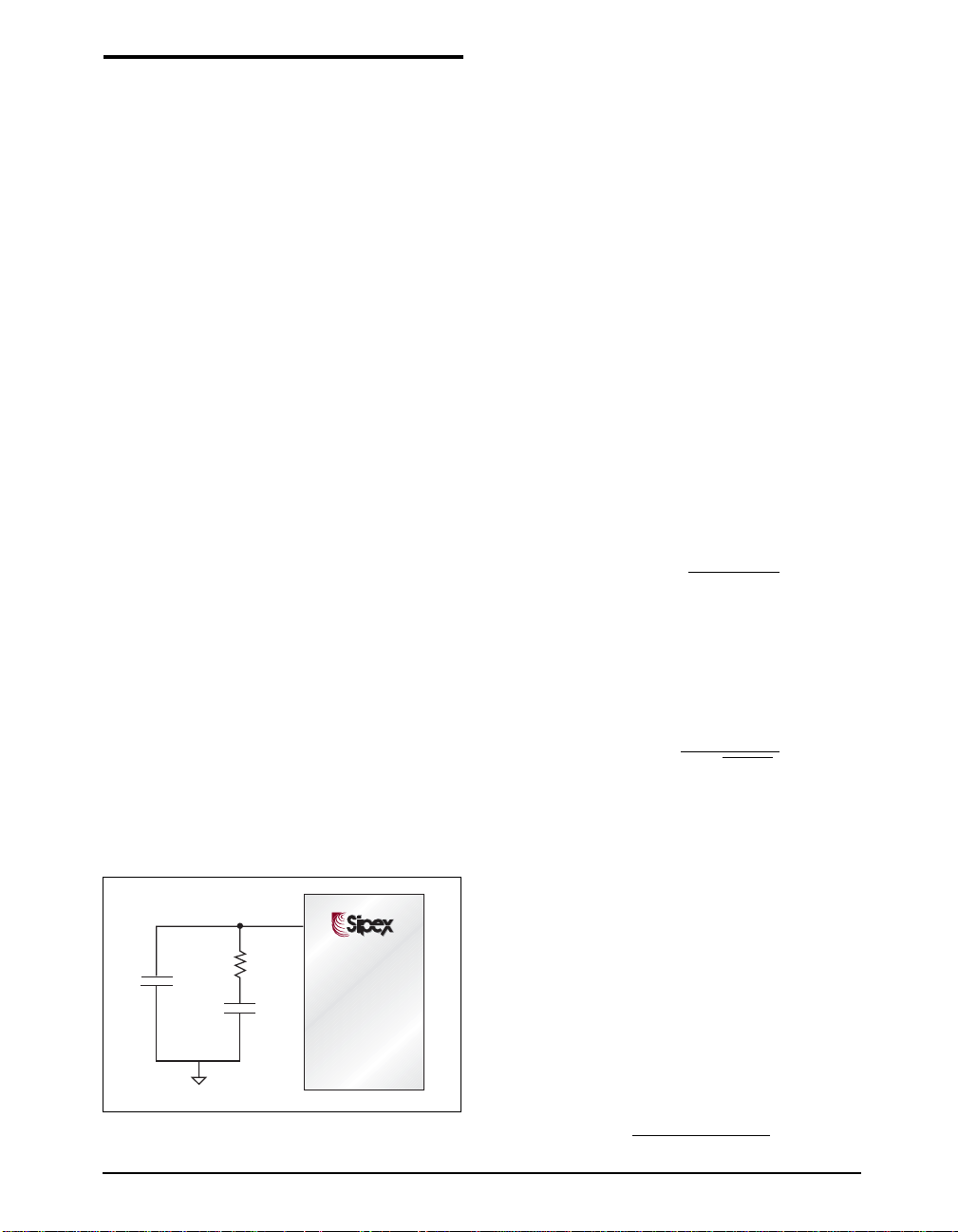
has a transconductance error amplifier and requires the compensation network to be connected between the COMP pin and ground, as
shown in Figure 18.
The first step of compensation design is to pick
the loop crossover frequency. High crossover
Schottky Diode Selection
When paralleled with the bottom MOSFET, an
optional Schottky diode can improve efficiency
and reduce noises. Without this Schottky diode,
the body diode of the bottom MOSFET conducts
the current during the non-overlap time when both
MOSFETs are turned off. Unfortunately, the body
diode has high forward voltage and reverse recovery problem. The reverse recovery of the body
diode causes additional switching noises when the
diode turns off. The Schottky diode alleviates
these noises and additionally improves efficiency
thanks to its low forward voltage. The reverse
frequency is desirable for fast transient response,
but often jeopardize the system stability. Since
the SP6120 is equipped with 3% window comparator that takes over the control loop on transient, the crossover frequency can be selected
primarily to the satisfaction of system stability.
Crossover frequency should be higher than the
ESR zero but less than 1/5 of the switching
frequency. The ESR zero is contributed by the
ESR associated with the output capacitors and
can be determined by:
1
f
=
Z(ESR)
2πC
OUTRESR
voltage across the diode is equal to input voltage,
and the diode must be able to handle the peak
current equal to the maximum load current.
Crossover frequency of 20kHz is a sound first
try if low ESR tantalum capacitors or poscaps
are used at the output. The next step is to calcuThe power dissipation of the Schottky diode is
determined by
P
DIODE
= 2VFI
OUTTNOLFS
late the complex conjugate poles contributed by
the LC output filter,
1
f
=
P(LC)
2π√ LC
OUT
where
T
= non-overlap time between GH and GL.
NOL
VF = forward voltage of the Schottky diode.
The open loop gain of the whole system can be
divided into the gain of the error amplifier,
PWM modulator, buck converter, and feedback
resistor divider. In order to crossover at the
selected frequency fco, the gain of the error
®
COMP
®
amplifier has to compensate for the attenuation
caused by the rest of the loop at this frequency.
C2
R1
SP6120
C1
In the RC network shown in Figure 18, the
product of R1 and the error amplifier
transconductance determines this gain. There-
fore, R1 can be determined from the following
equation that takes into account the typical error
amplifier transconductance, reference voltage
and PWM ramp built into the SP6120.
1300V
Figure 18. The RC network connected to the COMP pin
provides a pole and a zero to control loop.
Date: 1/19/05 SP6120 Low Voltage, AnyFETTM, Synchronous, Buck Controller © Copyright 2005 Sipex Corporation
R1 =
OUT fCO fZ(ESR)
V
IN fP(LC)
2
17
Page 18
f
APPLICATIONS INFORMATION: Continued
In Figure 18, R1 and C1 provides a zero f
which needs to be placed at or below f
is made equal to f
for convenience, the
P(LC)
P(LC)
. If f
value of C1 can be calculated as
2πf
1
P(LC)R1
C1 =
The optional C2 generates a pole fP1 with R1 to
cut down high frequency noise for reliable operation. This pole should be placed one decade
higher than the crossover frequency to avoid
erosion of phase margin. Therefore, the value of
the C2 can be derived from
C2 =
1
20πfCOR
1
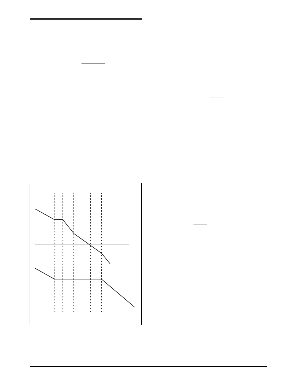
Figure 19 illustrates the overall loop frequency
response and frequency of each pole and zero.
To fine-tune the compensation, it is necessary to
physically measure the frequency response using a network analyzer.
Gain
-20db/dec
-40db/dec
Loop
-20db/dec
-20db/dec
f
Error Amplifier
fZ1f
P(LC)fZ(ESR)fCOfP1
Figure 19. Frequency response of a stable system and its
error amplifier.
-20db/dec
Current Sense
Z1
Z1
The SP6120 allows sensing current using the
inductor, PCB trace or current-sense resistor.
Inductor-sense utilizes the voltage drop across
the ESR of the inductor, while PCB trace and
current-sense resistor introduce additional resistance in series with the inductor. The resistance of the sense element determines the
overcurrent protection threshold as follows,
43mV
LIM
=
R
SEN
I
R
= current-sense resistance which can be
SEN
implemented as ESR of the inductor, trace or
discrete resistor.
The maximum power dissipation on the currentsense element is:
=
2
(max)
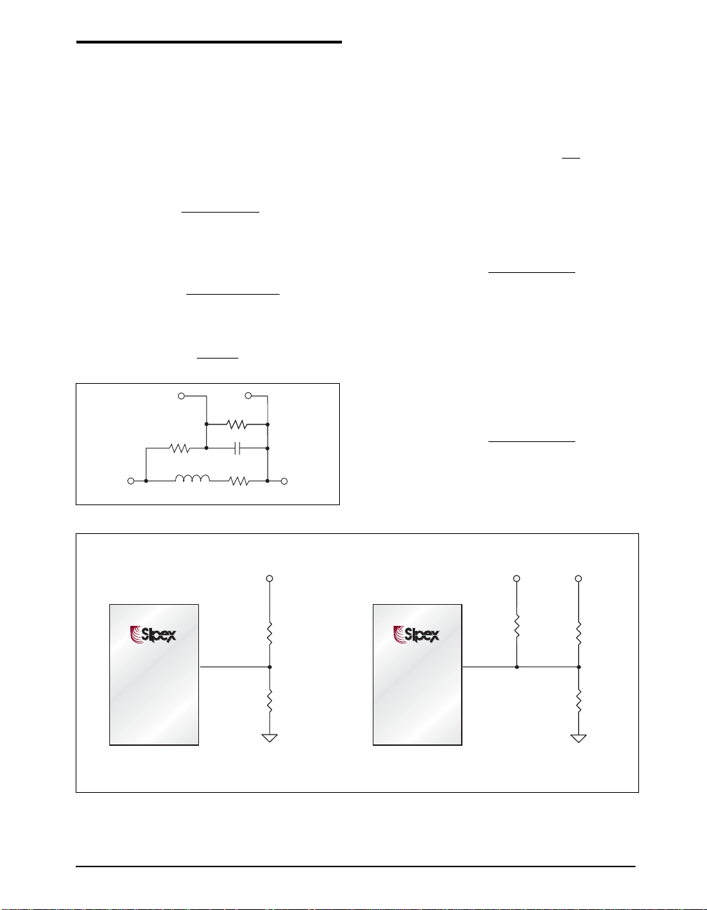
For the inductor-sense scheme shown in the
application circuit, RS and CS are used to replicate the signal across the ESR of the inductor. R
and CS can be looked at as a low pass filter
whose output represents the DC differential
voltage between the switch node and the output.
At steady state, this voltage happens to be the
output current times the ESR of the inductor. In
addition, if the following relationship is satisfied,
ESR
L
= RSC
S
the output of the RsCs filter represents the exact
voltage across the ESR, including the ripple.
Since the SP6120’s hiccup overcurrent protection scheme is intended to safeguard sustained
overload conditions, the DC portion of the current signal is more of interest. Therefore, designing the RSCS time constant higher than L/ESR
provides reliable current sense against any premature triggering due to noise or any transient
conditions. Pick Rs between 10k and 100k, and
Cs can be determined by:
CS = 2
L1
ESR R
Here the time constant of RSCS is twice the value
of L/ESR.
RIP
SENOUTSEN
S
S
Date: 1/19/05 SP6120 Low Voltage, AnyFETTM, Synchronous, Buck Controller © Copyright 2005 Sipex Corporation
18
Page 19
T
S
ISP
ISN
APPLICATIONS INFORMATION: Continued
In some applications, it may be desirable to
extend the current sense capability of a given
R
element (usually the inductor ESR) be-
SEN
yond the limit set by the 43mV threshold.
A straight forward way to do this would be to
add a resistor R
in parallel with CS, creating a
S2
voltage divider with RS. This changes the relationship with RS and CS to be
L1
= 2
C
S
ESR R
//R
S
S2
Using a voltage divider across the inductor, the
new relationship becomes:
I
=
LIM
43mV RS + R
ESR R
S2
S2
To calculate RS2, the formula becomes
I
ESR
RS2 = R
WN
Figure 20: Current Sensing
S
(
/
43mV
R
S
L
LIM
R
C
ESR
– 1
)
S2
S
V
OU
Output Voltage Programming
As shown in Figure 21(A), the voltage divider
connecting to the VFB pin programs the output
voltage according to
R
V
= 1.25( 1 +
OUT
1
)
R
2
where 1.25V is the internal reference voltage.
Select R2 in the range of 10k to 100k, and R1 can
be calculated using
R1 =
R2(V
OUT
1.25
– 1.25)
For output voltage less than 1.25V, a simple
circuit shown in Figure 21(B) can be used in
which V
is an external voltage reference
REF
greater than 1.25V. For simplicity, use the same
resistor value for R1 and R2, then R3 is determined as follows,
(V
– 1.25)R
R3 =
REF
2.5 – V
1
OUT
V
SP6120
> 1.25V
OUT
®
®
V
FB
R1
SP6120
®
®
V
V
FB
REF
V
< 1.25V
OUT
R3
R1
R2R2
AB
Figures 21(A), a voltage divider connected to the VFB pin programs the output voltageand 21(B), a simple circuit using
one external voltage reference programs the output voltages to less than 1.25V.
Date: 1/19/05 SP6120 Low Voltage, AnyFETTM, Synchronous, Buck Controller © Copyright 2005 Sipex Corporation
19
Page 20

APPLICATIONS INFORMATION: Continued
Layout Guideline
PCB layout plays a critical role in proper function of the converters and EMI control. In switch
mode power supplies, loops carrying high di/dt
give rise to EMI and ground bounces. The goal
of layout optimization is to identify these loops
and minimize them. It is also crucial on how to
connect the controller ground such that its operation is not affected by noise. The following
guideline should be followed to ensure proper
operation.
1. A ground plane is recommended for minimizing noises, copper losses and maximizing
heat dissipation.
2. Connect the ground of feedback divider, compensation components, oscillator resistor and
soft-start capacitor to the GND pin of the IC.
Then connect this pin as close as possible to
the ground of the output capacitor.
3. The VCC bypass capacitor should be right
next to the Vcc and GND pin.
5. Connect the PGND pin close to the source of
the bottom MOSFET, and the SWN pin to the
source of the top MOSFET. Minimize the
trace between GH/GL and the gates of the
MOSFETs. All of these requirements reduce
the impedance driving the MOSFETs. This is
especially important for the bottom MOSFET
that tends to turn on through its miller capacitor when the switch node swings high.
6. Minimize the loop composed of input capacitors, top/bottom MOSFETs and Schottky diode, This loop carries high di/dt current. Also
increase the trace width to reduce copper
losses.
7. Maximize the trace width of the loop connecting the inductor, output capacitors,
Schottky diode and bottom MOSFET.
4. The traces connecting to feedback resistor
and current sense components should be short
and far away from the switch node, and switching components.
Date: 1/19/05 SP6120 Low Voltage, AnyFETTM, Synchronous, Buck Controller © Copyright 2005 Sipex Corporation
20
Page 21
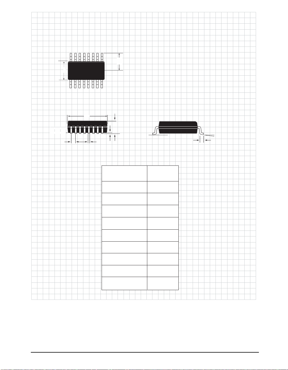
E1
PACKAGE: PLASTIC THIN SMALL
OUTLINE
(TSSOP)
E2
D
A
Ø
Be
A1
DIMENSIONS
in inches (mm)
Minimum/Maximum
A
A1
B
D
E1
e
E2
L
Ø
16–PIN
- /0.043
(- /1.10)
0.002/0.006
(0.05/0.15)
0.007/0.012
(0.19/0.30)
0.193/0.201
(4.90/5.10)
0.169/0.177
(4.30/4.50)
0.026 BSC
(0.65 BSC)
0.126 BSC
(3.20 BSC)
0.020/0.030
(0.50/0.75)
0°/8°
L
Date: 1/19/05 SP6120 Low Voltage, AnyFETTM, Synchronous, Buck Controller © Copyright 2005 Sipex Corporation
21
Page 22

ORDERING INFORMATION
Model Operating Temperature Range Package Type
SP6120CY ............................................... 0˚C to +70˚C ........................................ 16-Pin TSSOP
SP6120CY/TR ......................................... 0˚C to +70˚C ....................................... 16-Pin TSSOP
SP6120EY .............................................. -40˚C to +85˚C ...................................... 16-Pin TSSOP
SP6120EY/TR.........................................-40˚C to +85˚C ..................................... 16-Pin TSSOP
Available in lead free packaging. To order add "-L" suffix to part number.
Example: SP6120EY/TR = standard; SP6120EY-L/TR = lead free
/TR = Tape and Reel
Pack quantity is 1,500 for TSSOP.
CLICK HERE TO ORDER SAMPLES
Corporation
ANALOG EXCELLENCE
Sipex Corporation
Headquarters and
Sales Office
233 South Hillview Drive
Milpitas, CA 95035
TEL: (408) 934-7500
FAX: (408) 935-7600
Sipex Corporation reserves the right to make changes to any products described herein. Sipex does not assume any liability arising out of the
application or use of any product or circuit described herein; neither does it convey any license under its patent rights nor the rights of others.
Date: 1/19/05 SP6120 Low Voltage, AnyFETTM, Synchronous, Buck Controller © Copyright 2005 Sipex Corporation
22
 Loading...