

Page 1
查询SP6661EN供应商
SP6661
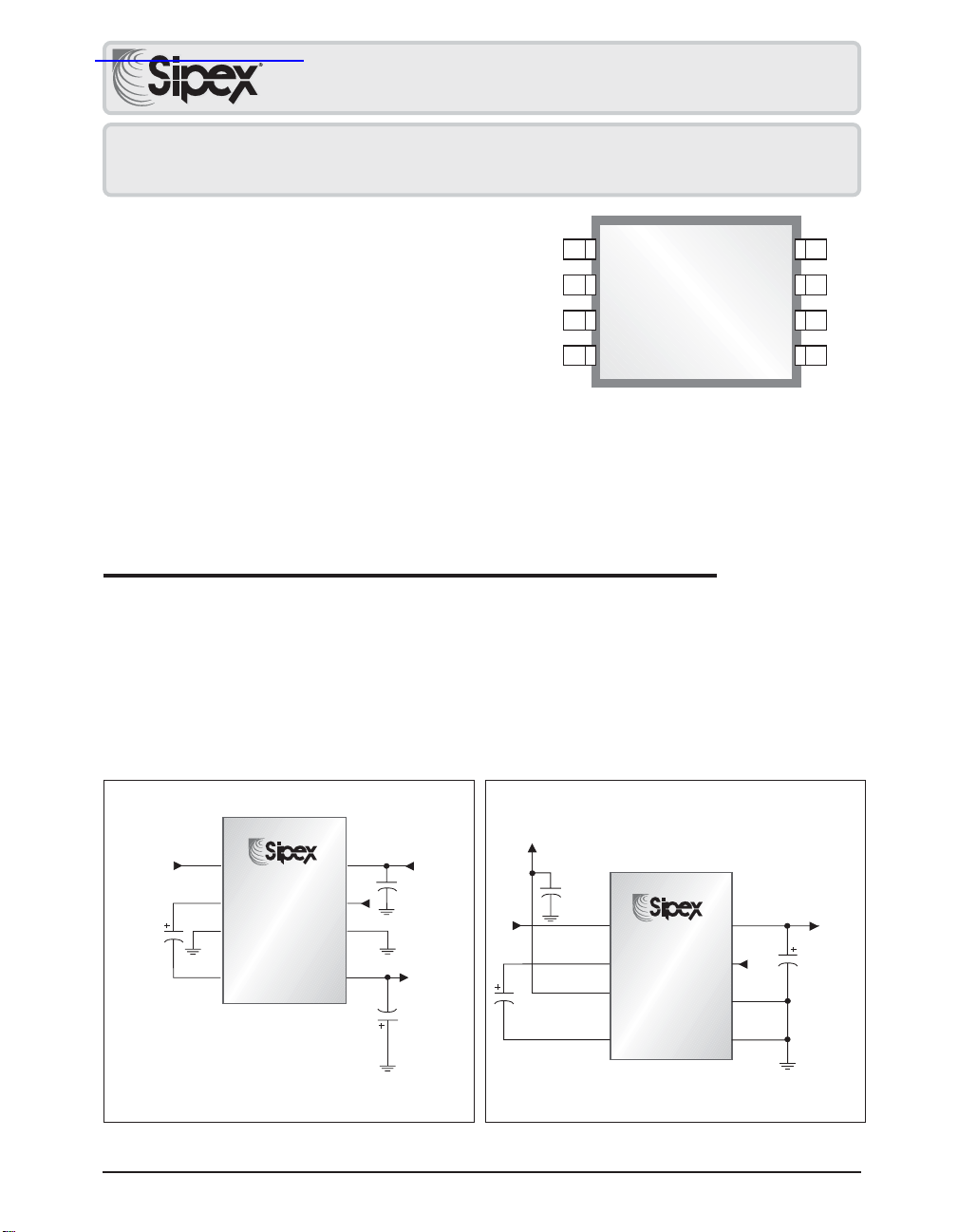
High Frequency 200mA Charge Pump
Inverter or Doubler
■ Inverts or Doubles Input Supply Voltage
1
■ 92% Power Efficiency at 100mA
■ 120kHz/900kHz Selectable Oscillator Fre-
quency
■ 4.5Ω Output Resistance Using 3.3µF Ceramic
Caps
■ Low Voltage Battery Operation
FC
CAP+
GND
CAP-
2
3
SP6661
8 Pin nSOIC
4
■ Ideal for 3.6V Lithium Ion Battery or 5.0V Input
■ High Output Current – 200mA
Now Available in Lead Free Packaging
■ Low Profile Solution
■ 1.5V Inverter Startup Guaranteed
■ Pin-Compatible High-Current Upgrade of the
ICL7660 and 660 Industry Standard
■ Smallest Package Available for the 660
Industry Standard – 8 pin µSOIC
DESCRIPTION
The SP6661 is a CMOS DC-DC Monolithic Voltage Converter that can be implemented as a
Voltage Inverter or a Positive Voltage Doubler. As a Voltage Inverter, a -1.5V to -5.0V output can
be converted from a +1.5V to +5.0V input. As a Voltage Doubler, a +5.0V to +10.0V output can
be provided from a +2.5V to +5.0V input. The SP6661 is ideal for both battery-powered and board
level voltage conversion applications with a typical operating current of 3mA and a high efficiency
(>90%) over most of its load-current range. Typical end products for this device are disk drive
supplies, operational amplifier and interface power supplies, medical instruments, and hand held
and laptop computers. The SP6661 is available in 8-pin NSOIC, and µSOIC packages.
8
7
6
5
V+
OSC
LV
OUT
+V
IN
+2.5V to +5.0V
C3
1µF to 22µF
CAP+
GND
CAP-
1
2
3
4
FC
C1
1µF to 22µF
Figure 2: Voltage Doubler
SP6661
®
+V
8
7
OSC
LV
6
OUT
5
DOUBLE
NEGATIVE
VOLTAGE
OUTPUT
C2
1µF to 22µF
C1
1µF to 22µF
®
+V
8
OSC
7
LV
6
OUT
5
CAP+
GND
CAP-
1
2
3
4
SP6661
FC
+V
IN
+1.5V to +5.0V
C3
1µF to 22µF
INVERTED
NEGATIVE
VOLTAGE
OUTPUT
C2
1µF to 22µF
Figure 1: Voltage Inverter
Date: 05/25/04 SP6661 High Frequency 200mA Charge Pump Inverter or Doubler © Copyright 2004 Sipex Corporation
1
Page 2
ABSOLUTE MAXIMUM RATINGS
These are stress ratings only and functional operation
of the device at these ratings or any other above those
indicated in the operation sections of the specifications
below is not implied. Exposure to absolute maximum
rating conditions for extended periods of time may
affect reliability.
Power Supply Voltage
(V+ to GND or GND to OUT).............................+5.6V
LV Input Voltages............(OUT - 0.3V) to (V+ + 0.3V)
FC and OSC Input Voltages......The least negative of
(OUT - 0.3V) or (V+ - 5.6V) to (V+ + 0.3V)
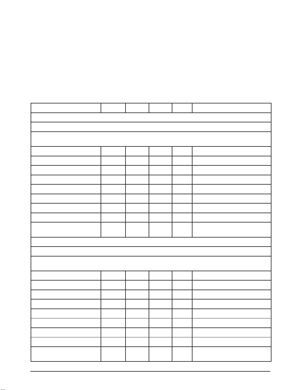
SPECIFICATIONS
RETEMARAP.NIM.PYT.XAMSTINUSNOITIDNOC
2etoN
egnaRegatloVylppuS5.13.5VR
egatloVpU-tratS39.0V
tnerruCylppuS36AmdaoLoN
tnerruCtuptuOxaM002Am
tnerruCtupnIrotallicsO1±Aµ
ycneuqerFrotallicsO07021071zHk
ecnatsiseRtuptuO57
ycneiciffEnoisrevnoCegatloV0.999.99%daoLoN
ycneiciffErewoP08
07
98
28
OUT and V+ Continuous Output Current.........200mA
Output Short-Circuit Duration to GND (Note 1).......1s
Operating Temperature Ranges
SP6661E_...........................-40˚C to +85˚C
Continuous Power Dissipation (T
NSOIC
(derate 5.88mW/˚C above +70˚C).......471mW
= 70˚C)
AMB
µSOIC (derate 4.10mW/˚C above +70˚C)........330mW
Operating Temperature.......................-40˚C to +85˚C
Storage Temperature........................-65˚C to +150˚C
Lead Temperature (soldering 10s)..................+300˚C
sroticapaCFµ22htiwycneuqerFwoLtatiucriCretrevnI
T,DNG=VL,nepo=CF,Fµ22=3C=2C=1C,V0.5+=+V
T=
BMA
Tot
NIM
Ω
I
L
I
L
%
I
L
XAM
L
otrefer; 1erugiF .tiucrictset
005= Ω
3etoN,Am001=
Am001=
Am002=
sroticapaCFµ22htiwycneuqerFwoLtatiucriCrelbuoD
T,DNG=VL,nepo=CF,Fµ22=3C=2C=1C,V0.5+=+V
T=
2etoN
BMA
Tot
NIM
egnaRegatloVylppuS5.23.5VR
XAM
L
otrefer; 22erugiF .tiucrictset
k1= Ω
egatloVpU-tratS5.1V
tnerruCylppuS36AmdaoLoN
tnerruCtuptuOxaM002Am
tnerruCtupnIrotallicsO1±Aµ
ycneuqerFrotallicsO07021071zHk
ecnatsiseRtuptuO5.47
Ω
I
L
3etoN,Am001=
ycneiciffEnoisrevnoCegatloV0.999.99%daoLoN
ycneiciffErewoP98
97
Date: 05/25/04 SP6661 High Frequency 200mA Charge Pump Inverter or Doubler © Copyright 2004 Sipex Corporation
49
09
I
L
%
I
L
Am001=
Am002=
2
Page 3
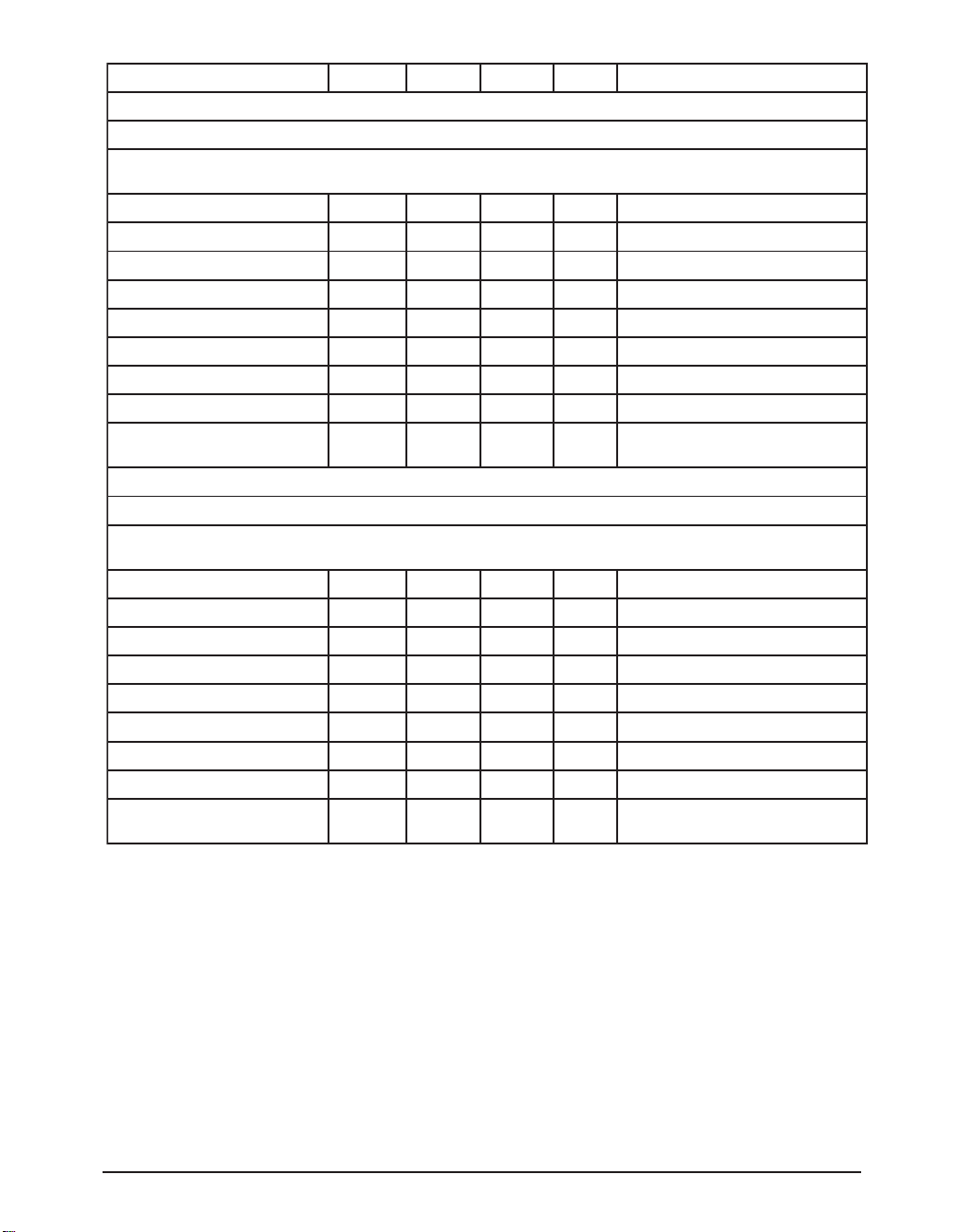
SPECIFICATIONS (continued)
RETEMARAP.NIM.PYT.XAMSTINUSNOITIDNOC
sroticapaCFµ3.3htiwycneuqerFhgiHtatiucriCretrevnI
T,DNG=VL,+V=CF,Fµ3.3=3C=2C=1C,V0.5+=+V
T=
2etoN
BMA
Tot
NIM
egnaRegatloVylppuS5.13.5VR
egatloVpU-tratS39.0V
tnerruCylppuS0181AmdaoLoN
tnerruCtuptuOxaM002Am
tnerruCtupnIrotallicsO8±Aµ
ycneuqerFrotallicsO0050090521zHk
ecnatsiseRtuptuO57
Ω
ycneiciffEnoisrevnoCegatloV0.996.99%daoLoN
ycneiciffErewoP87
56
48
97
%
sroticapaCFµ3.3htiwycneuqerFhgiHtatiucriCrelbuoD
T,DNG=VL,+V=CF,Fµ3.3=3C=2C=1C,V0.5+=+V
T=
2etoN
BMA
Tot
NIM
egnaRegatloVylppuS5.23.5VR
egatloVpU-tratS5.1V
tnerruCylppuS0181AmdaoLoN
tnerruCtuptuOxaM002Am
tnerruCtupnIrotallicsO8±Aµ
ycneuqerFrotallicsO0050090521zHk
ecnatsiseRtuptuO5.47
Ω
ycneiciffEnoisrevnoCegatloV0.999.99%daoLoN
ycneiciffErewoP78
97
29
98
%
NOTE 1: Specified output resistance is a combination of internal switch resistance and capacitor ESR.
NOTE 2: In the test circuit capacitors C1, C2 and C3 are 22µF, 0.05 maximum ESR, ceramic or 3.3µF, 0.05Ω
maximum ESR, ceramic. Capacitors with higher ESR may reduce output voltage and efficiency. Refer to Capacitor
Selection section.
NOTE 3: Specified output resistance is a combination of internal switch resistance and capacitor ESR. Refer to
Optimizing Capacitor Selection.
XAM
I
L
I
L
I
L
XAM
I
L
I
L
I
L
L
L
otrefer; 1erugiF .tiucrictset
005= Ω
3etoN,Am001=
Am001=
Am002=
otrefer; 2erugiF .tiucrictset
k1= Ω
3etoN,Am001=
Am001=
Am002=
Date: 05/25/04 SP6661 High Frequency 200mA Charge Pump Inverter or Doubler © Copyright 2004 Sipex Corporation
3
Page 4
Optimizing Capacitor Selection
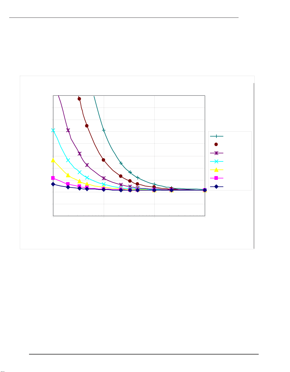
Refer to Figure 1 for the total output resistance for various capacitance values and oscillator frequencies.
The reservoir and charge pump capacitor values are equal. The capacitance values required to maintain
comparable ripple and output resistance typically diminish proportionately as the pump frequency of
the SP6661 increases.
20
18
16
14
12
10
10KHz
20KHz
50KHz
100KHz
8
6
200KHz
500KHz
1000KHz
4
2
0
110100 1000
Total Output Source Resistance Vs C1, C2
C1, C2 Capacitance (uF)
Figure 1. Total Output Resistance for various capacitance values and oscillator frequencies.
Date: 05/25/04 SP6661 High Frequency 200mA Charge Pump Inverter or Doubler © Copyright 2004 Sipex Corporation
4
Page 5
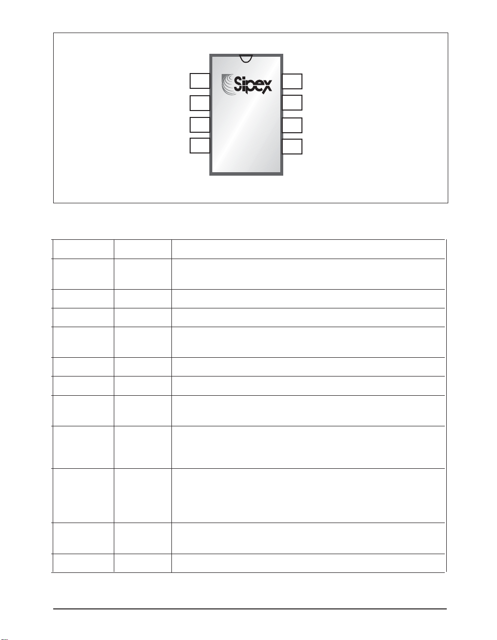
PINOUT
FC
®
1
8
V+
CAP+
GND
CAP-
PIN ASSIGNMENTS
Pin Number Pin Symbol Description
1FCFrequency Control for the internal oscillator. FC = open,
2 CAP+ Connect to the positive terminal of the charge pump capacitor.
3 GND (Voltage Inverter Circuit) Ground.
3 GND (Positive Voltage Doubler Circuit) Positive supply voltage
4 CAP- Connect to the negative terminal of the charge pump capacitor.
5 OUT (Voltage Inverter Circuit) Negative voltage output pin.
2
SP6661
3
4
f
= 120kHz typical; FC = V+ f
osc
input.
7
6
5
OSC
LV
OUT
= 900kHz typical.
osc
5 OUT (Positive Voltage Doubler Circuit) Ground pin for power
supply.
6LVLow -voltage operation input pin in 660 circuits. In SP6661
circuits can be connected to GND, OUT or left open as desired
with no effect.
7 OSC Control pin for the oscillator. Internally connected to 15pF
capacitor. An external capacitor can be added to slow the
oscillator. Be careful to minimize stray capacitance. An
external oscillator can be connected to overdrive the OSC pin.
8V+(Voltage Inverter Circuit) Positive voltage input pin for the
power supply.
8V+ (Positive Voltage Doubler Circuit) Positive voltage output.
Date: 05/25/04 SP6661 High Frequency 200mA Charge Pump Inverter or Doubler © Copyright 2004 Sipex Corporation
5
Page 6
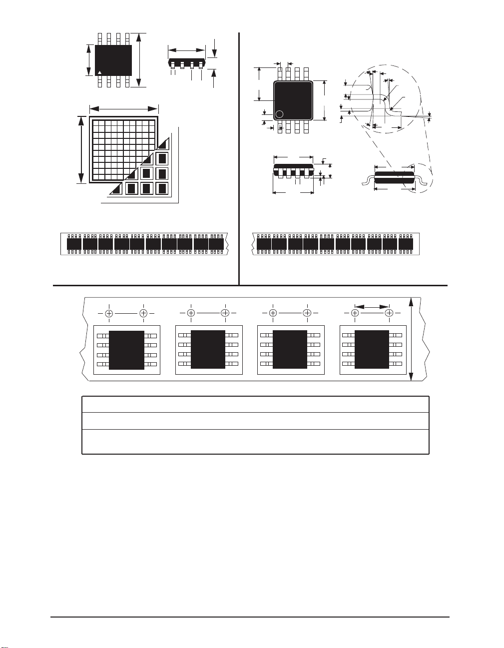
All package dimensions in inches
0.189/0.197
0.228/0.2440.150/0.157
0.014/0.019
1
0.050 BSC
0.053/0.069
0.0965
±0.003
2
0.020
0.020
2
1
0.013
±0.005
2
0.116
±0.004
0.118
±0.004
0.0256
BSC
0.118
±0.004
0.004
±0.002
0.034
±0.004
0.040
±0.003
100 die per waffle pack
95 NSOIC devices per tube, no minimum quantity 50 µSOIC devices per tube
0.012
±0.003
0.16
±0.003
R .003
12.0˚
±4˚
12.0˚
±4˚
0.008
0˚ - 6˚
0.006
±0.006
0.006
±0.006
0.0215
0.01
±0.006
0.037
Ref
0.116
±0.004
0.118
±0.004
3.0˚
±3˚
P
W
8-pin NSOIC 13” reels: P = 8mm, W = 12mm
pkg min qty per reel std qty per reel max qty per reel
CN 500 1500 2500
CU 500 1500 3000
Date: 05/25/04 SP6661 High Frequency 200mA Charge Pump Inverter or Doubler © Copyright 2004 Sipex Corporation
6
Page 7
ORDERING INFORMATION
Part Number Temperature Range Package Type
SP6661EN . ............................................ -40˚C to +85˚C ......................................... 8-Pin NSOIC
SP6661EN/TR ........................................ -40˚C to +85˚C ......................................... 8-Pin NSOIC
SP6661EU . ............................................ -40˚C to +85˚C ......................................... 8-Pin µSOIC
SP6661EU/TR ........................................ -40˚C to +85˚C ......................................... 8-Pin µSOIC
SP6661UEB ...................................................................................8-Pin µSOIC Evaluation Board
Available in lead free packaging. To order add "-L" suffix to part number.
Example: SP6661EN/TR = standard; SP6661EN-L/TR = lead free
/TR = Tape and Reel
Pack quantity is 2500 for NSOIC.
ANALOG EXCELLENCE
Sipex Corporation
Headquarters:
233 Hillview Dr
Milpitas, CA 95035
TEL: (408) 934-7500
FAX: (408) 935-7600
Sipex Corporation reserves the right to make changes to any products described herein. Sipex does not assume any liability arising out of the
application or use of any product or circuit described herein; neither does it convey any license under its patent rights nor the rights of others.
Date: 05/25/04 SP6661 High Frequency 200mA Charge Pump Inverter or Doubler © Copyright 2004 Sipex Corporation
7
 Loading...