

Page 1
®
Advanced
SP6687
4 Channel Charge Pump White LED Driver
C2P
C2N
13
14
15
16
GND
12
11
SP6687
16 Pin QFN
1
2
EN
FEATURES
■ High Efficiency > 90%
■ Support up to 4 White LEDs with current
matching
■ Three Charge Pump Modes: X1, X1.5, X2
■ Soft Start Function
■ Short Circuit Protection
■ Output Overvoltage Protection
■ Thermal Shutdown
■ Programmable LED drive capability
■ PWM Dimming Control
■ 1MHz Fixed Frequency Oscillator
■ Low 1µA Shutdown Current
■ Pin Compatible with SC604
LED4
LED3
LED2
LED1
Pin 1
Orientation
Now Available in Lead Free Packaging
APPLICATIONS
■ Mobile phones
■ White LED Backlighting
■ Camera Flash LED lighting
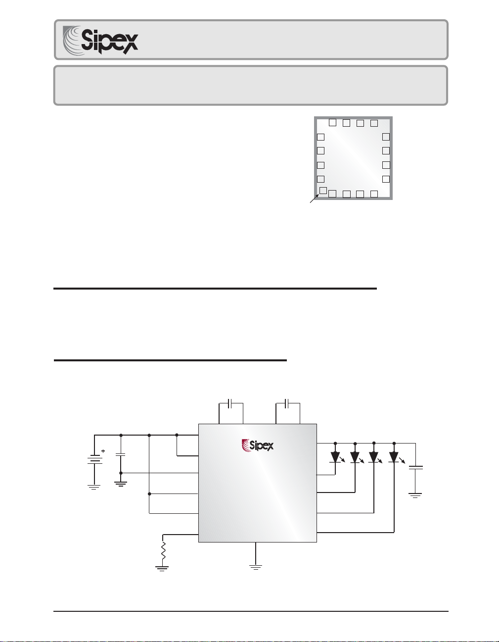
The SP6687 is a compact, highly efficient and highly integrated 4 channel charge pump white LED
driver. It can support from 1 to 4 White LEDs and is optimized for Li-Ion battery applications.
Current matching allows all 4 LEDs to maintain consistent brightness. Users can control White
LEDs by three programming bits. Each channel can support up to 30mA of current. This device
is available in a 4mm x 4mm, 16 pin QFN package.
TYPICAL APPLICATION CIRCUIT
CTRL0
C1N
10
9
8
C1P
7
VIN
6
VOUT
5
ISET
4
3
CTRL1
CTRL2
DESCRIPTION
GND
C2 1µF
1011
C2N
V
OUT
LED1
LED2
LED3
LED4
6
C
16
15
14
13
OUT
1µF
®
12
Li-ion
Battery
C
1µF
C1 1µF
89
C1N C2P
C1P
7
V
IN
IN
R
SET
1
2
3
4
5
EN
CTRL0
CTRL1
CTRL2
I
SET
SP6687
Typical Application Circuit for 4-White LEDs
Date: 04/20/05 SP6687 4Channel Charge Pump White LED Driver © Copyright 2005 Sipex Corporation
1
Page 2

These are stress ratings only and functional operation of the device at these ratings or any other above those indicated in the operation sections of the
specifications below is not implied. Exposure to absolute maximum rating conditions for extended periods of time may affect reliability.
Input Voltage.....................................................-0.3 to 6V
Output Voltage..................................................-0.3 to 6V
Power Dissipation, PD @ TA = 25ºC
QFN-16L 4x4...........................................................2.5W
Package Thermal Resistance
QFN-16L 4x4, OJA................................................40ºC/W
Junction Temperature Range...............-40ºC to 125ºC
Storage Temperature .........................-65ºC to 150°C
Operating Temperature ....................... -40°C to 85°C
ESD Susceptibility
Human Body Model...............................................2kV
Machine Mode.....................................................200V
ABSOLUTE MAXIMUM RATINGS
Unless otherwise specified: V
PARAMETER MIN TYP MAX UNITS CONDITIONS
Input Supply Voltage 2.5 5.5 V
Under Voltage Lockout Threshold 1.8 2.2 2.4 V V
Under Voltage Lockout Hysteresis 50 mV
Current into LEDs
1, 2, 3, and 4
Quiescent Current 3 4 mA F
Quiescent Current in Shutdown 1 10 µAV
Accuracy (Note 1) 2 7.5 % 2mA < I
I
LED
Current Matching (Note 2) 1 5 % 2mA < I
1x mode to 1.5x mode Transition
Voltage (V
Falling)
IN
1.5x mode to 2x mode Transition
Voltage (V
Falling)
IN
= 2.85V to 5.5V, C1 = C2 =1.0µF (ESR = 0.03Ω, TA = 25°C)
IN
Rising
IN
18.5 20 21.5 mA R
4.5 5 5.5 mA R
SET
SET
220mA2.7V < V
230mA3.1V < V
OSC
= 4.5V, En Pin = ZeroV
IN
V
LED
3.75 3.85 V
I
LED1
20mA
V
LED
2.65 2.8 V
I
LED1
20mA
ELECTRICAL CHARACTERISTICS
= 24.0kΩ
= 91.0kΩ
< 5.5V
IN
< 5.5V
IN
= 1MHz, I
< 30mA
LED
< 30mA
LED
= 3.5V, I
= I
=I
LED2
= 3.5V, I
= I
= I
LED2
OUT
= 80mA
OUT
LED3
= 80mA
OUT
LED3
= 0mA
= I
LED4
= I
LED4
=
=
Oscillator Frequency 0.8 1.0 1.2 MHz
Input Current Limit 250 400 650 mA
Short Circuit applied from
to GND
V
OUT
Open circuit at any LED that
Output Over Voltage Protection 5.5 6 V
is programmed to be in the
ON state
Date: 04/20/05 SP6687 4Channel Charge Pump White LED Driver © Copyright 2005 Sipex Corporation
2
Page 3
Unless otherwise specified: V
RETEMARAPNIMPYTXAMSTINUSNOITIDNOC
ELECTRICAL CHARACTERISTICS
= 2.85V to 5.5V, C1 = C2 =1.0µF (ESR = 0.03Ω, TA = 25°C)
IN
dlohserhThgiHtupnI5.1V
dlohserhTwoLtupnI4.0V
tnerruChgiHtupnI1AµV
tnerruCwoLtupnI1AµVLIDNG=
dlohserhTnwodtuhSlamrehT041051081Cº
siseretsyHnwodtuhSlamrehT01Cº
I
Note 1:
I
LED(ERR) =
LED(MEA) - ILED(SET)
I
LED(SET)
X 100%
Note 2: Current Matching refers to the difference in current from one LED to the next.
I
(I
Current Matching
LED
LED(MAX) - ILED(MIN)
I
LED(MAX) + ILED(MIN)
X 100%)
C1P C1N C2P C2N
V
IN
GND
1x/1.5x/2x
Charge Pump
1MHz
1MHz
Oscillator
dlohserhtcigoLhgiHtupnI
)2LRTC,1LRTC,0LRTC,NE(
dlohserhtcigoLwoLtupnI
)2LRTC,1LRTC,0LRTC,NE(
HIV=NI
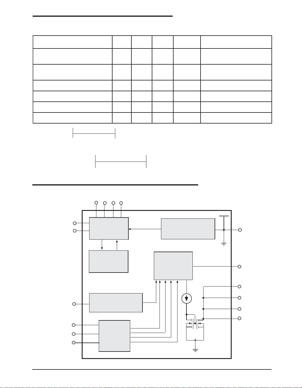
FUNCTIONAL DIAGRAM
VOUT
Mode
Decision
I-Setting
I
SET
ISET
LED1
I
EN
Bandgap
V
REF
SET
LED2
LED3
LED4
CTRL0
CTRL1
CTRL2
Date: 04/20/05 SP6687 4Channel Charge Pump White LED Driver © Copyright 2005 Sipex Corporation
Decoder
306mV
3
Page 4
#NIPEMANNIPNOITPIRCSED
1NE)hgiHevitcA(elbanEpihC
20LRTC)1elbateeS(0tiBlortnoCtuptuO
31LRTC)1elbateeS(1tiBlortnoCtuptuO
42LRTC)1elbateeS(2tiBlortnoCtuptuO
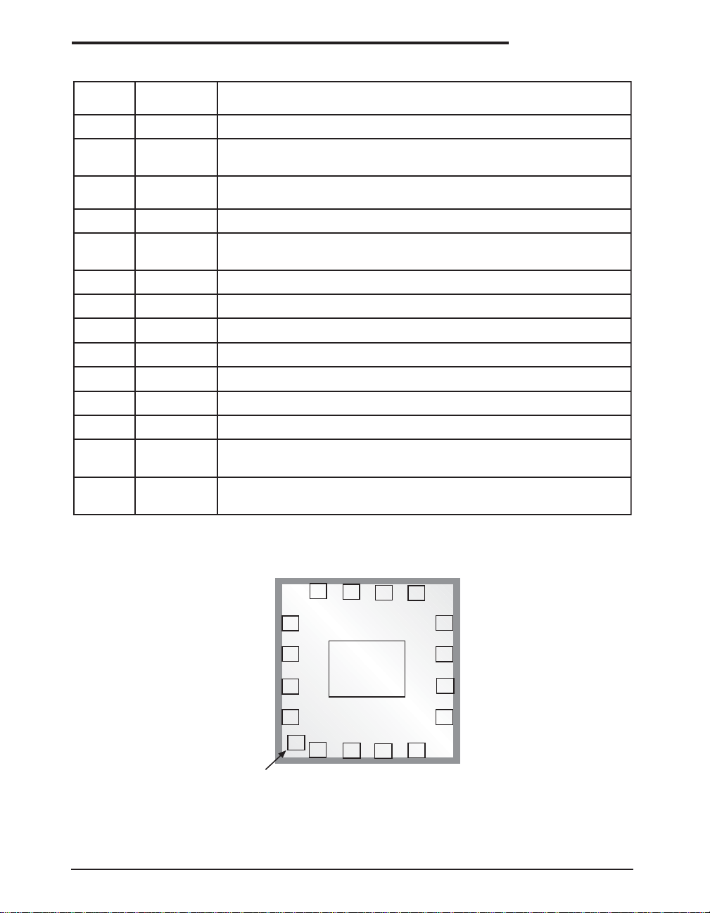
PIN DESCRIPTION
5I
6V
7V
TES
TUO
NI
8P1C1roticapaCtekcuBfolanimreTevitisoP
9N1C1roticapaCtekcuBfolanimreTevitageN
01N2C2roticapaCtekcuBfolanimreTevitageN
11P2C2roticapaCtekcuBfolanimreTevitisoP
21DNGdnuorG
61ot314ot1DEL
desopxE
daP
DNG DNGotdetcennocdnadraobBCPotderedlosebdluohsdapdesopxE
LED4
13
RrotsiserehtfoeulavehtybtessitnerrucDEL
IehttrohstonoD.dnuorgot
TES
TES
IrofegatloV.nip
TES
Iehtmorfdetcennoc
nip
TES
.V1.1yllacipytsi
.sedonaDELehtotnoitcennocrofecruoSegatloVtuptuO
egatloVtupnIrewoP
ro,dednuorg,nepotfelebyamnip,esunitonfI(.DELrofkniStnerruC
Votdetcennoc
)
NI
C2P
11
10
C2N
9
C1N
8
C1P
GND
12
LED3
14
7
VIN
GND
4
CTRL2
6
VOUT
5
ISET
LED2
LED1
Pin 1
Orientation
15
16
1
2
3
EN
CTRL0
CTRL1
TOP VIEW
Date: 04/20/05 SP6687 4Channel Charge Pump White LED Driver © Copyright 2005 Sipex Corporation
4
Page 5
The SP6687 is a high efficiency charge pump white
LED driver. It provides 4 channels of low drop-out
voltage current source to regulate the current for 4
white LEDs. For high efficiency, the SP6687
implements 3 modes of charge pump: x1/x1.5/x2
modes. An external R
is used to set the current
SET
level of the White LEDs. SP6687 has an input current
regulation circuit to reduce the input ripple.
Soft Start
The SP6687 includes a soft start circuit to limit the
inrush current at power on and mode switching. The
soft start circuit holds the input current level long
enough for output capacitor C
to reach a desired
OUT
voltage level. When the soft start turns off, the SP6687
will not sink current spiking from VIN.
Mode Decision
The SP6687 uses a smart mode decision method to
select the working mode for maximum efficiency. The
mode decision circuit senses the output and LED
voltage for up/down selection.
Dimming Control
CTRL0, CTRL1 and CTRL2 are used to control the
on/off of correlated White LEDs. When an external
PWM signal is connected to the control pin, the
brightness of the white LEDs is adjusted by the duty
cycle.
LED Current Setting
The current flowing through White LEDs connected
to the SP6687 can be set by R
. Every current that
SET
flows through each respective White LED is 440
times greater than the current of R
. The white LED
SET
current can be estimated by following equation:
THEORY OF OPERATION
I
LED
ISET
=1.1V, and R
to GND.
SET
=440x (
V
ISET
R
SET
where V
nected from I
Thermal Shutdown
The SP6687 provides a high current capability to drive
4 white LEDs. A thermal shutdown circuit is needed to
protect the chip from thermal damage. When the chip
reaches the shutdown temperature of 150ºC, the
thermal shutdown circuit turns off the chip to prevent
thermal accumulation in the chip.
Overvoltage Protection
SP6687 regulates the output voltage by controlling
the input current. When the output voltage reaches the
designated level, SP6687 reduces the input current.
Subsequently, the output voltage regulation also serves
as an overvoltage protection circuit.
Short Circuit Protection
A current limiting circuit is also included in the SP6687
for short circuit protection. Whenever the output
sources a dangerously high current, the current limiting circuit takes over the output regulation circuit and
reduces the output current to an acceptable level.
is the resistance con-
SET
)
APPLICATION INFORMATION
SP6687
GND
12
C2 1µF
C2P
®
1011
C2N
V
OUT
LED1
LED2
LED3
LED4
6
C
16
15
14
13
OUT
1µF
Li-ion
Battery
C
1µF
C1 1µF
89
C1N
C1P
7
V
IN
IN
R
SET
1
2
3
4
5
EN
CTRL0
CTRL1
CTRL2
I
SET
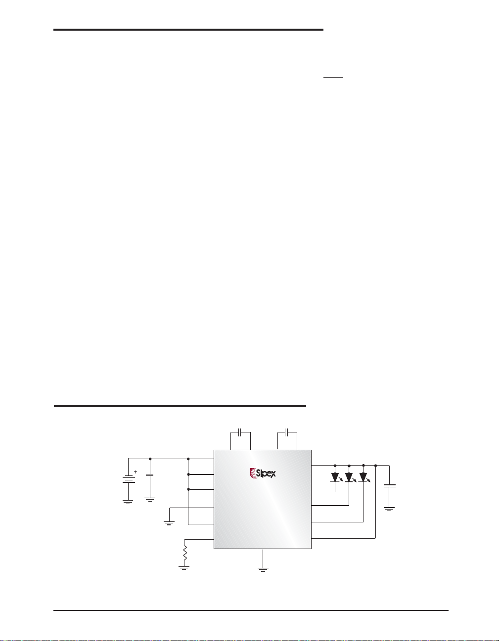
Typical Application Circuit For 3-White LEDs
Date: 04/20/05 SP6687 4Channel Charge Pump White LED Driver © Copyright 2005 Sipex Corporation
5
Page 6
APPLICATION INFORMATION
9
SP6687
GND
C2 1µF
11
10
C2N
6
V
®
OUT
16
LED1
15
LED2
14
LED3
13
LED4
12
Li-ion
Battery
C
1µF
C1 1µF
8
C1P
V
IN
EN
CTRL0
CTRL1
CTRL2
I
SET
C1N C2P
7
IN
R
SET
1
2
3
4
5
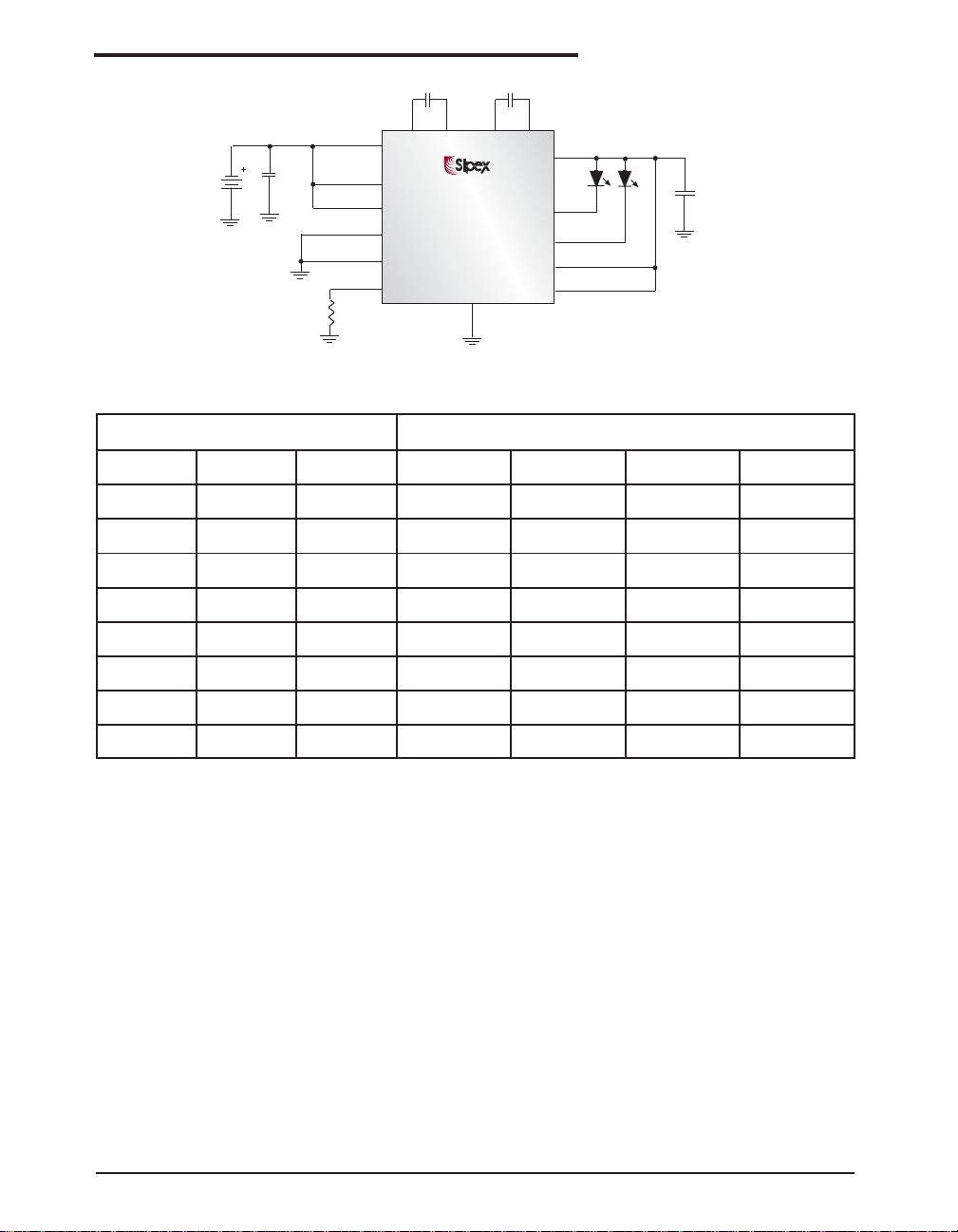
Typical Application Circuit for 2-White LEDs
stupnIlortnoCsutatStuptuO
2LRTC1LRTC0LRTC4DEL3DEL2DEL1DEL
000 FFOFFOFFONO
001 FFOFFONOFFO
010 FFONOFFOFFO
011 NOFFOFFOFFO
100 FFOFFONONO
C
1µF
OUT
101 FFONONONO
110 NONONONO
111 FFOFFOFFOFFO
Table 1. Typical application circuit for PWM dimming
using a DC voltage into I
Date: 04/20/05 SP6687 4Channel Charge Pump White LED Driver © Copyright 2005 Sipex Corporation
SET.
6
Page 7
APPLICATION INFORMATION
Selecting Capacitors
To get better performance from the SP6687, the selection of appropriate capacitors is very important. These
capacitors determine some parameters such as input
and output ripple, power efficiency, maximum supply
current by the charge pump and start up time. To reduce
the input and output ripple effectively, low ESR ceramic
capacitors are recommended.
Generally to reduce output ripple, increasing the output
capacitance C
is necessary. However, this will in-
OUT
crease the startup time of the output voltage.
For LED driver applications, the input voltage ripple is
more important than output ripple. Input ripple is controlled by the input capacitor CIN -- increasing the value
of input capacitance can further reduce the ripple. Practically, the input voltage ripple depends on the impedance of the power supply. If a single input capacitor C
cannot satisfy the requirement of the application, it is
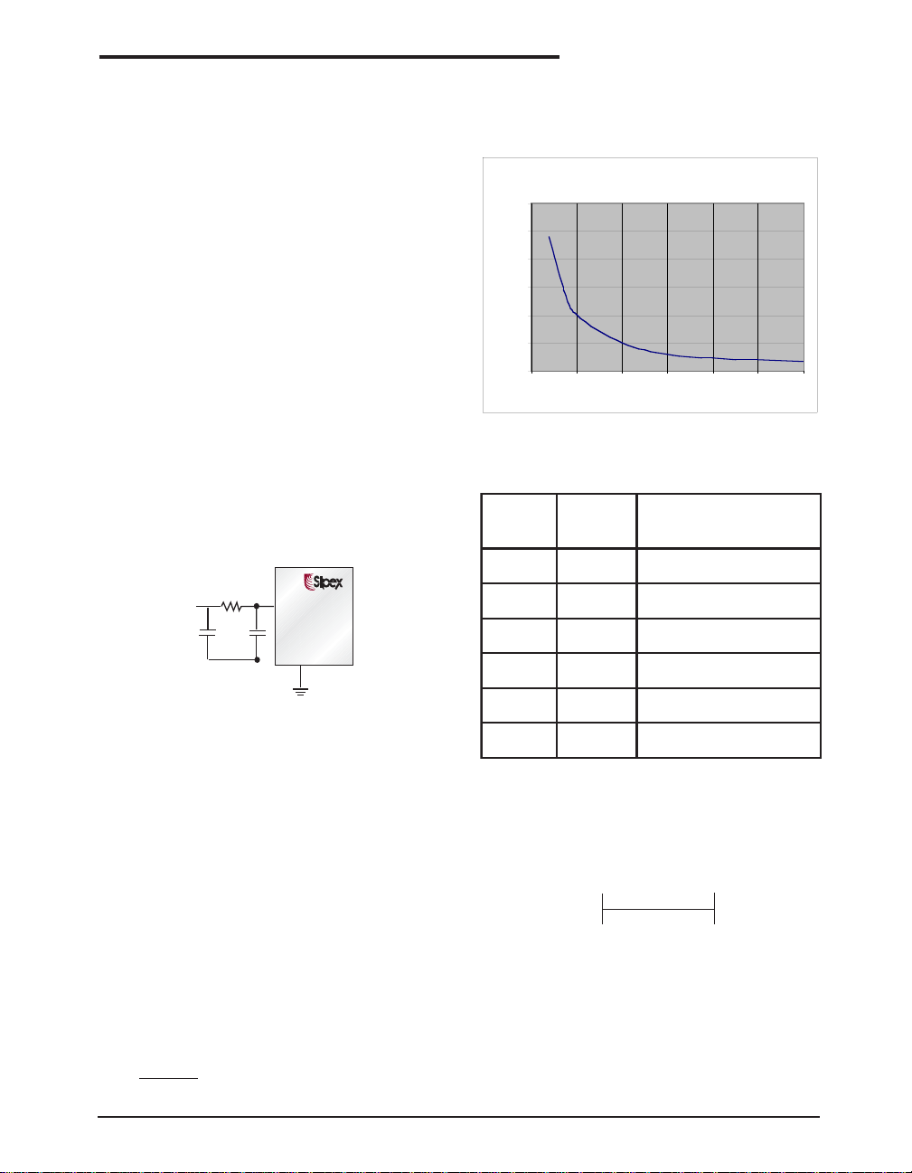
necessary to add a low-pass filter. Figure 1 shows a CR-C filter used on the SP6687. The input ripple can be
reduced to less than 30mVp-p when driving 80mA of
output current.
1.0Ω
V
IN
2.2µF2.2µF
V
IN
®
SP6687
Figure 2 shows the typical value of R
LED current and Table 2 shows the values of R
fixed LED current.
Typical Curve for R
300
250
Ω
200
150
100
RSET Value (k_)
50
0
051015 20 25 30
Figure 2. The typical curve of R
IN
vs. Avg. LED Current
SET
LED Current (mA)
average current.
I
DEL
R
TES
)Am(
Ω
)k(
50.190.19
019.745.74
517.234.23
versus average
SET
vs. LEDs
SET
SET
for a
dradnatStseraeN
)k(TESRrofeulaV
Ω
020.420.42
Figure 1. C-R-C filter used to reduce input ripple.
526.916.91
034.615.61
The flying capacitors C1 and C2 determine the supply
current capability of the charge pump and influence the
overall efficiency of the system. Lower values will im-
Table 2. R
Value Selection
SET
prove efficiency, but will limit the current to the LEDs at
low input voltages. For 4 X 20mA load over the entire
input range of 2.7 to 5.5V, a capacitor of 1µF is optimal.
If maximum accuracy is required, a precision resistor is
needed. The following equation shows how to calculate
Setting the LED Current
The SP6687 can be set to a fixed LED current by a
resistor R
connected from I
SET
to GND. R
SET
SET
establishes the reference current and mirrors the current into
LED1, LED2, LED3, and LED4. The current into each
LED is about 440 times the current that flows through
R
. The approximate setting formula is given as
SET
the error: I
Where I
LED(MEAS)
I
is the LED current which is determined by R
LED(SET)
LED(ERR)
= I
LED(MEAS)
I
LED(SET)
- I
LED(SET)
is practical measured LED current and
X 100%
SET.
follows:
484(V)
R
(Ω)
SET
I
=
LED
Date: 04/20/05 SP6687 4Channel Charge Pump White LED Driver © Copyright 2005 Sipex Corporation
7
Page 8
APPLICATION INFORMATION
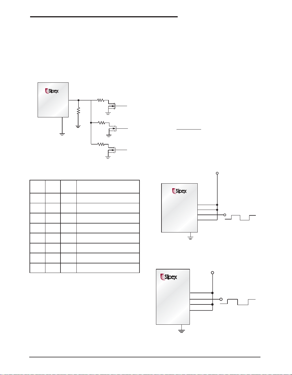
LED Current Setting with NMOS
LED current setting control can also be achieved by using
an external NMOS transistor to change the equivalent
resistor of the I
pin. Figure 3 illustrates this application
SET
circuit which has 3 bit signals and can set 8 different levels
of LED current. Table 3 shows the relation between the
equivalent resistor of the I
pin and the respective
SET
control signal.
®
SP6687
ISET
R4
R1
S1
R2
S2
R3
S3
Figure 3. Typical application circuit for setting LED
current using an NMOS transistor to set R
1S2S3S
000 R
001 R
010 R
011 R
100 R
10 1 R
110 R
111 R
TESR=1
TESR=2
TESR=1
TESR=1
R(
TESR=4
TESR=3
TESR=2
TESR=1
)
TES
R//
R//
R//3R//
R//
R//3R//
R//2R//
R//2R//3R//
SET
4
4
4
nip
IforetsiseRtnelaviuqE
TES
4
4
4
4
LED Dimming Control Methods
The SP6687 uses two methods to achieve LED dimming control. These methods are detailed below.
PWM Dimming
The first dimming method utilizes a PWM control signal
into CTRL0, CTRL1, and CTRL2. Table 1 shows the
relation between CTRLx and the 4 LED current states.
For example, when CTRL1 and CTRL2 are at logic high
and CTRL0 receives a PWM signal then 4 LEDs will be
dimmed simultaneously. The average LED current can
be derived by using a known PWM signal value. When
the PWM signal logic is low the current can be set at a
fixed value with the R
resistor. The following equation
SET
will give the approximate value of the LED current:
X I
T
OFF
I
=
LED(AVG)
Where T
T
PWM
is the time of the PWM signal at low. I
OFF
LED(ON)
T
PWM
is the period of the PWM dimming signal.
is LED on
LED(ON)
state current.
V
IN
®
SP6687
CTRL2
CTRL1
CTRL0
EN
PWM
LED
OFF
LED
ON
Figure 4. Typical application circuit for PWM dimming
when driving 4 LEDs
®
.
V
IN
Table 3. Control signal and equivalent resistor of the
I
pin.
SET
SP6687
CTRL2
CTRL1
CTRL0
EN
PWM
LED
OFF
LED
ON
Figure 5. Typical application circuit for PWM dimming
when driving 3 LEDs
Date: 04/20/05 SP6687 4Channel Charge Pump White LED Driver © Copyright 2005 Sipex Corporation
.
8
Page 9
APPLICATION INFORMATION
V
IN
®
SP6687
CTRL2
CTRL1
CTRL0
PWM
EN
LED
OFF
LED
ON
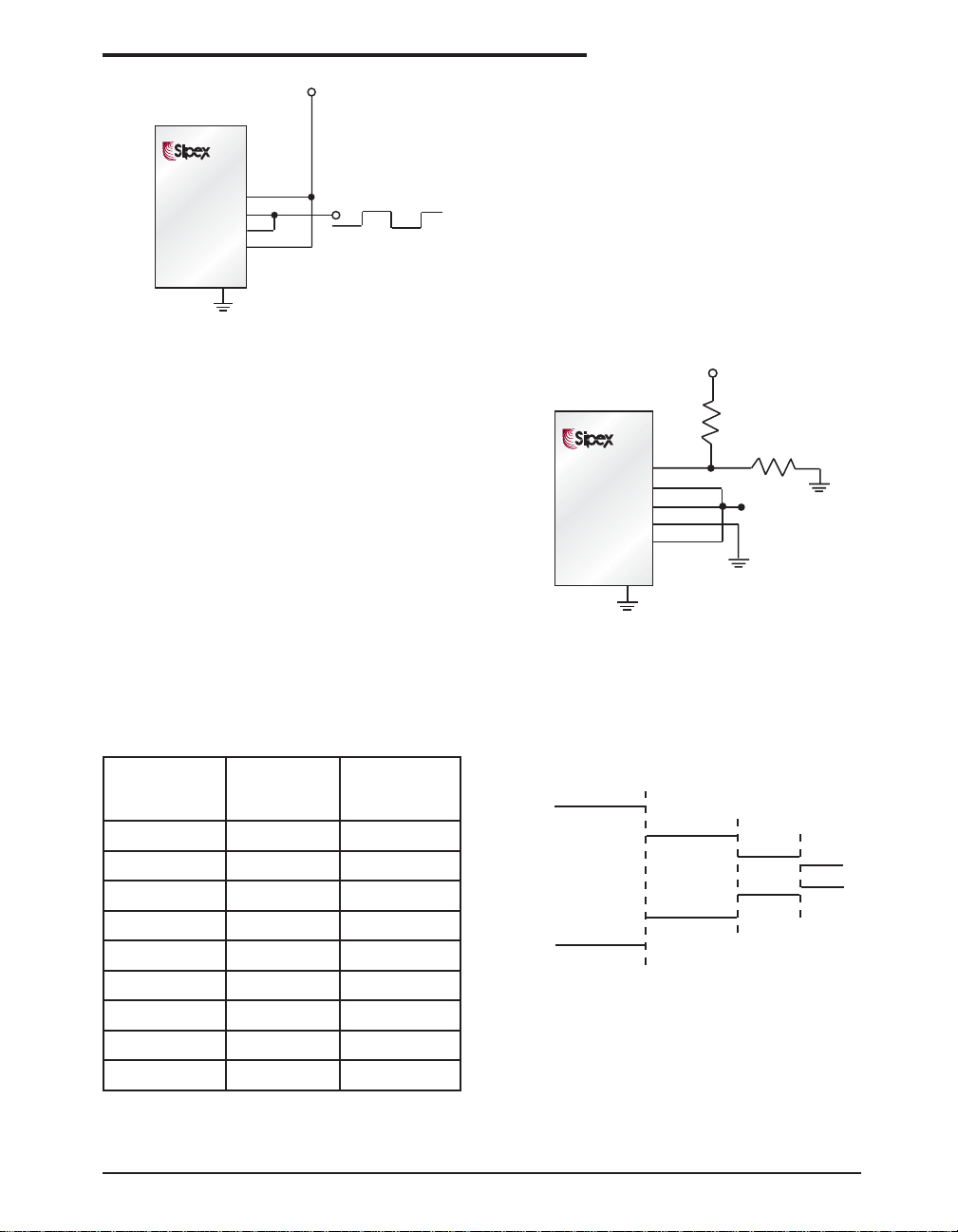
Figure 6. Typical application circuit for PWM dimming
when driving 2 LEDs
.
Due to the 100µs delay time between mode transfers,
the duty cycle of the dimming frequency should not
exceed the maximum duty cycle on the CTRLx pins.
For best performance it is recommended to keep the
dimming frequency between 200Hz and 1kHz. When
the duty cycle is exceeded, the SP6687 cannot transfer modes properly. The following equation shows the
relation between maximum duty of the CTRLx pins
and the PWM dimming frequency:
-6
D
=(1-100 x10
MAX
Where D
MAX
x FD)
is the Maximum Duty of CTRLX and FD is
the PWM Dimming Frequency.
Dimming using a DC voltage added to I
Using an analog input voltage
that connects to the I
VADJ
pin is another method for
SET
SET
via a resistor R
ADJ
dimming control of LEDs. Figure 7 shows the application circuit. For this application the LED current can be
derived from the following equation:
I
= 440 X [1.1 x (1/R
LED
SP6687
®
ISET
CTRL2
CTRL1
CTRL0
+ 1/R
SET
EN
) - V
ADJ
V
ADJ
R
ADJ
R
SET
V
IN
ADJ/RADJ
]
Figure 7. Typical application circuit for PWM dimming
using a DC voltage into I
SET.
gnimmiD
)zH(ycneuqerF
K109.001.0
00919.090.0
00829.080.0
00739.070.0
00649.060.0
00559.050.0
00469.040.0
XLRTC
mumixaM
ytuD
DELI
ytuDmuminiM
V
ADJ
2.5V
1.6V
LED
I
0.8V
13mA
6.5mA
0V
20mA
0mA
Figure 8. SP6687 dimming control application using a
DC voltage into I
SET.
00379.030.0
00289.020.0
Table 4. Dimming frequency relative to Min/Max duty
Date: 04/20/05 SP6687 4Channel Charge Pump White LED Driver © Copyright 2005 Sipex Corporation
Figure 8 shows the relation between V
a typical application example, with V
.
RSET = 43k Ohms and R
= 55kOhms.
ADJ
and I
ADJ
from 0 to 2.5V,
ADJ
LED
of
9
Page 10
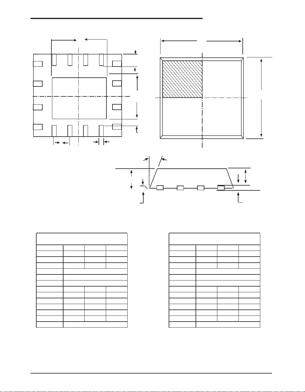
PACKAGE: 16 PIN QFN
D2
D
NX L
E2
E
NX K
e
NX b
4X غ
A2
A
SEATING PLANE
A1
A3
16 Pin QFN JEDEC MO-220 VGGC-4
SYMBOL
A 0.8 0.9 1
A1 0 0.02 0.05
A2 0 0.65 1
A3
D
E
E 7.4 7.8 8.2
D2 2.2 2.4 2.6
E2 2.2 2.4 2.6
L 0.45 0.55 0.65
K 0.2 - b 0.25 0.3 0.35
e
Note: Dimensions in (mm)
Controlling Dimension
Date: 04/20/05 SP6687 4Channel Charge Pump White LED Driver © Copyright 2005 Sipex Corporation
Variation
MIN NOM MAX
0.20 REF
4.00 BSC
4.00 BSC
0.65 BSC
16 Pin QFN JEDEC MO-220 VGGC-4
SYMBOL
A 0.0315 0.0354 0.0394
A1 0 0.0008 0.0020
A2 0 0.0256 0.0394
A3
D
E
E 0.2913 0.3071 0.3228
D2 0.0866 0.0945 0.1024
E2 0.0866 0.0945 0.1024
L 0.0177 0.0217 0.0256
K 0.0079 - b 0.0098 0.0118 0.0138
e
Note: Dimensions in (inches)
Conversion Factor: 1 Inch = 25.40 mm
Variation
MIN NOM MAX
0.0079 REF
0.1575 BSC
0.1575
0.0256 BSC
10
Page 11

ORDERING INFORMATION
Part Number Operating Temperature Range Package Type
SP6687ER1-L/TR....................................... -40°C to +85°C ........................................16 Pin 4mmx4mm QFN
Available in lead free packaging only.
-L = lead free
/TR = Tape and Reel
Pack quantity is 2,500 for QFN.
Corporation
ANALOG EXCELLENCE
Sipex Corporation
Headquarters and
Sales Office
233 South Hillview Drive
Milpitas, CA 95035
TEL: (408) 934-7500
FAX: (408) 935-7600
Sipex Corporation reserves the right to make changes to any products described herein. Sipex does not assume any liability arising out of the
application or use of any product or circuit described herein; neither does it convey any license under its patent rights nor the rights of others.
Date: 04/20/05 SP6687 4Channel Charge Pump White LED Driver © Copyright 2005 Sipex Corporation
11
 Loading...