

Page 1
For Audio Equiment
MN6475A
D/A Converter for Digital Audio Equipment
Overview
The MN6475A is a CMOS digital-to-analog converter
by noise shaping technology and is designed for PCM
digital audio equipment. It features a built-in 4 times
oversampling and 16-bit input digital filter.
It includes a digital de-emphasis circuit and analog post
filter to reduce the parts count and power consumption
of the overall D/A conversion system.
And also it includes two noise-shaping 1-bit D/A converters, one each for the left and right channels.
Features
Built-in 4 times oversampling digital filter
(Bandwidth ripple of ±0.051dB and attenuation
of 47.99dB dB)
Built-in second order analog post filter with a cutoff
frequency of 100 kHz
Built-in digital de-emphasis circuit with a deviation
between +0.47 dB and – 0.07 dB
Choice of normal or double-speed playback
Built-in overflow limiter
No zero cross distortion
Sample-and-hold circuit is unnecessary
Choice of 768fs or 384fs operation
Single 5V power supply
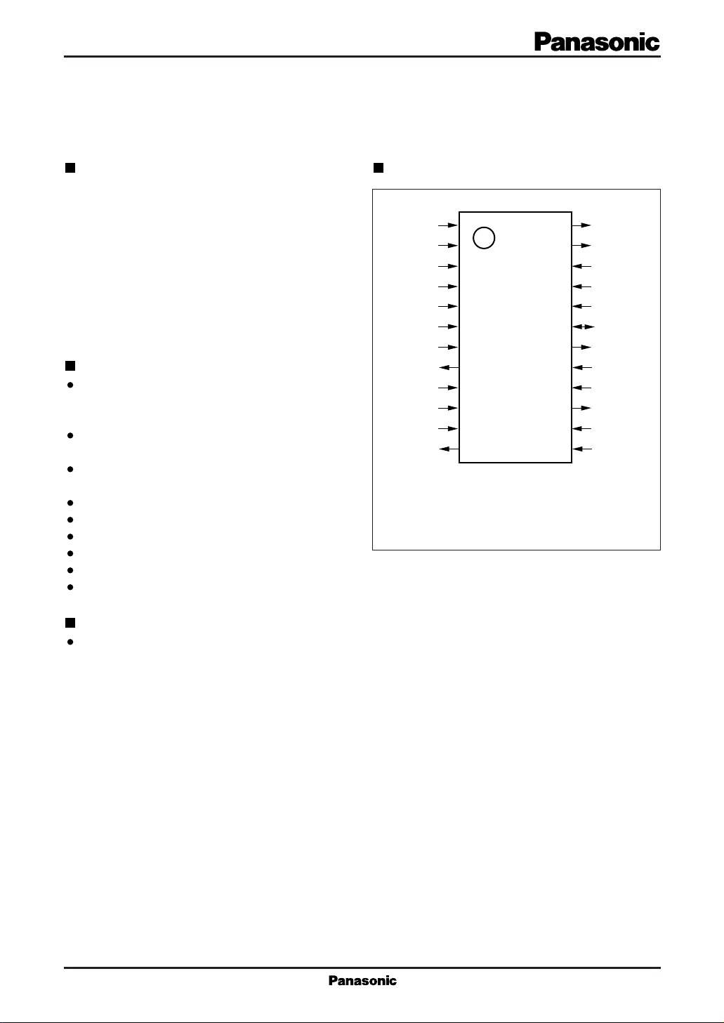
Pin Assignment
DD
1
2
3
4
5
6
7
8
9
10
SS
11
12
LRCLK
BCLK
SRDATA
COT1
COT2
TEST
V
X2
X1
V
V
DDL
OUTL
(TOP VIEW)
SOP024-P-0375
XOUT
24
COUT
23
CSEL
22
DEMPH
21
WVEL
20
TP
19
PWML
18
RSTB
17
V
16
15
14
13
DDR
OUTR
V
SSR
V
SSL
Applications
CD players and other digital audio equipment
Page 2
MN6475A For Audio Equipment
Block Diagram
WVEL
X1
X2
CSEL
COUT
XOUT
RSTB
TP
TEST
PWML
18
+
20
9
8
22
23
24
17
19
6
Timing gen.
PWM
Logic
OUTL
12
–+
(L)
LR selector
Noise shaping logic
4 times oversampling
Digital filter
Digital de-emphasis
S/P converter
OUTR
15
–
PWM
Logic
(R)
3
SRDATA
2
BCLK
1
LRCLK
21
DEMPH
Page 3

For Audio Equipment MN6475A
Pin Descriptions
Pin No. Symbol Function Description
1 LRCLK LRCLK input pin. "H" level; left channel data input
"L" level; right channel data
2 BCLK Bit clock input pin for serial data
3 SRDATA Serial data input pin
4 COT 1 L L
Stereo output
5 COT2 LHLH
Left channel
output only output only
H
Right channel
6 TEST LSI test mode pin. Keep this pin at "L" level.
7VDDPower supply pin for digital circuits (+5V)
8 X2 Crystal oscillator pin
9 X1 Crystal oscillator pin (external clock input pin)
10 V
11 V
SS
DDL
Ground pin for digital circuits (0V)
Power supply pin for left channel analog circuits (+5V)
12 OUTL Left channel analog signal output pin
13 V
14 V
SSL
SSR
Ground pin for left channel analog circuits (0V)
Ground pin for right channel analog circuits (0V)
15 OUTR Right channel analog signal output pin
16 V
DDR
Power supply pin for right channel digital circuits (+5V)
17 RSTB Reset pin (Active low).
Pull this pin low once after applying the power.
18 PWML LSI test output pin.
Leave this pin open.
19 TP Input/Output pin for LSI test mode. Keep this pin at "L" level.
20 WVEL Internal operation mode selection pin
21 DEMPH Digital De-emphasis ON/OFF pin. ON at "H" level.
22 CSEL Clock frequency selection pin for COUT pin output.
"L" level; 1/4 clock frequency from crystal oscillator or external clock signal
"H" level; 1/2 clock frequency
23 COUT Frequency-divided clock output
24 XOUT Output using frequency from crystal oscillator or external clock signal
H
Output with
channels
reversed
Page 4

MN6475A For Audio Equipment
Conversion Characteristics
VDD=5.0V, VSS=0V, f=33.8688MHz, Ta=25˚C
Parameter Symbol Test Conditions min typ max Unit
Analog characteristics *
Signal-to-noise ratio S/N EIAJ 97 104 dB dB
Dynamic range D.R. EIAJ 90 97 dB
Total harmonic distortion THD+N EIAJ 0.003 0.006 %
Crosstalk EIAJ 84 100 dB
Output level 1 *
Output level 2 *
Notes
*1: These analog characteristics are based on measurements in the application circuit example next page.
*2: This level is measured at point B in that circuit.
*3: This level is measured at point A (LSI output pin) in that circuit.
1
2
3
1kHz F.S. 2.0 2.3 2.6 V
1kHz F.S. 1.0 1.2 1.4 V
rms
rms
Page 5

For Audio Equipment MN6475A
Application Circuit Example
V
DDR
23
24
COUT
XOUT
22
CSEL
20
21
WVEL
DEMPH
19
TP
100Ω
18
PWML
SXSXSXSXSX
17
RSTB
16
DDR
V
47µF
–
+
–
+
1µF
15
OUTR
MN6475A
DD
BCLK
SRDATA
COT1
COT2
23456789101112 13
1 LRCLK
SX SX SX
4.7kΩ
TEST
X2X1VSSV
V
4.7kΩ
5pF 5pF
–
+
330µF
0.1µF
–
+
100µF
–
+
22µF
–
+
220µF
470µF
14
SSR
V
DDL
100Ω
A
SSL
V
OUTL
1µF
–
+
470µF
–
+
47µF
V
SS
0.001µF
A
0.001µF
2.2kΩ
2.2kΩ
1000pF
–
+
–
+
4.7kΩ 4.7kΩ
22µF
47kΩ
4.7kΩ 4.7kΩ
22µF
47kΩ
1200pF
1200pF
1000pF
+
–
18kΩ
+
–
18kΩ
18kΩ
18kΩ
560Ω
22µF
0.001µF
560Ω
22µF
0.001µF
B
47kΩ
B
47kΩ
V
DD
V
DDL
Page 6

MN6475A For Audio Equipment
Package Dimensions (Unit: mm)
SOP024-P-0375
±0.20
15.30
24
13
7.20±0.200.10±0.10 2.00±0.20
0.05
-
+0.10
0.15
1.10±0.20
0 to 10°
0.30min.
112
2.40max. 9.40±0.30
(0.67) 0.40
1.27
±0.10
SEATING PLANE
 Loading...