

Page 1
For Audio Equipment
MN6474A
D/A Converter for Digital Audio Equipment
Overview
The MN6474A is a CMOS digital-to-analog converter
with a built-in 16-bit digital filter for pulse code
modulation (PCM) digital audio equipment.
It uses noise shaping technology to convert a digital
signal into a PWM signal.
It contains a 4-fold oversampling digital filter that
permits simplification of the low pass filter after the D/A
converter, thus greatly reducing the power consumption
of the entire D/A conversion system.
The chip provides both regular and inverted phase
outputs for both channels.
The chip contributes to cost and size reductions for CD
players and other digital audio equipment.
Features
Built-in 4-fold oversampling digital filter
(ripple of only ±0.0072 dB within the supported
band and attenuation of 62.7 dB within the cutoff
band)
Internal resolution of 18 bits
Two's complement input (I2S input code also supported)
Built-in overflow limiter
No zero cross distortion
Sample-and-hold circuit is unnecessary
Output pin for detecting zero input
Single 5V power supply
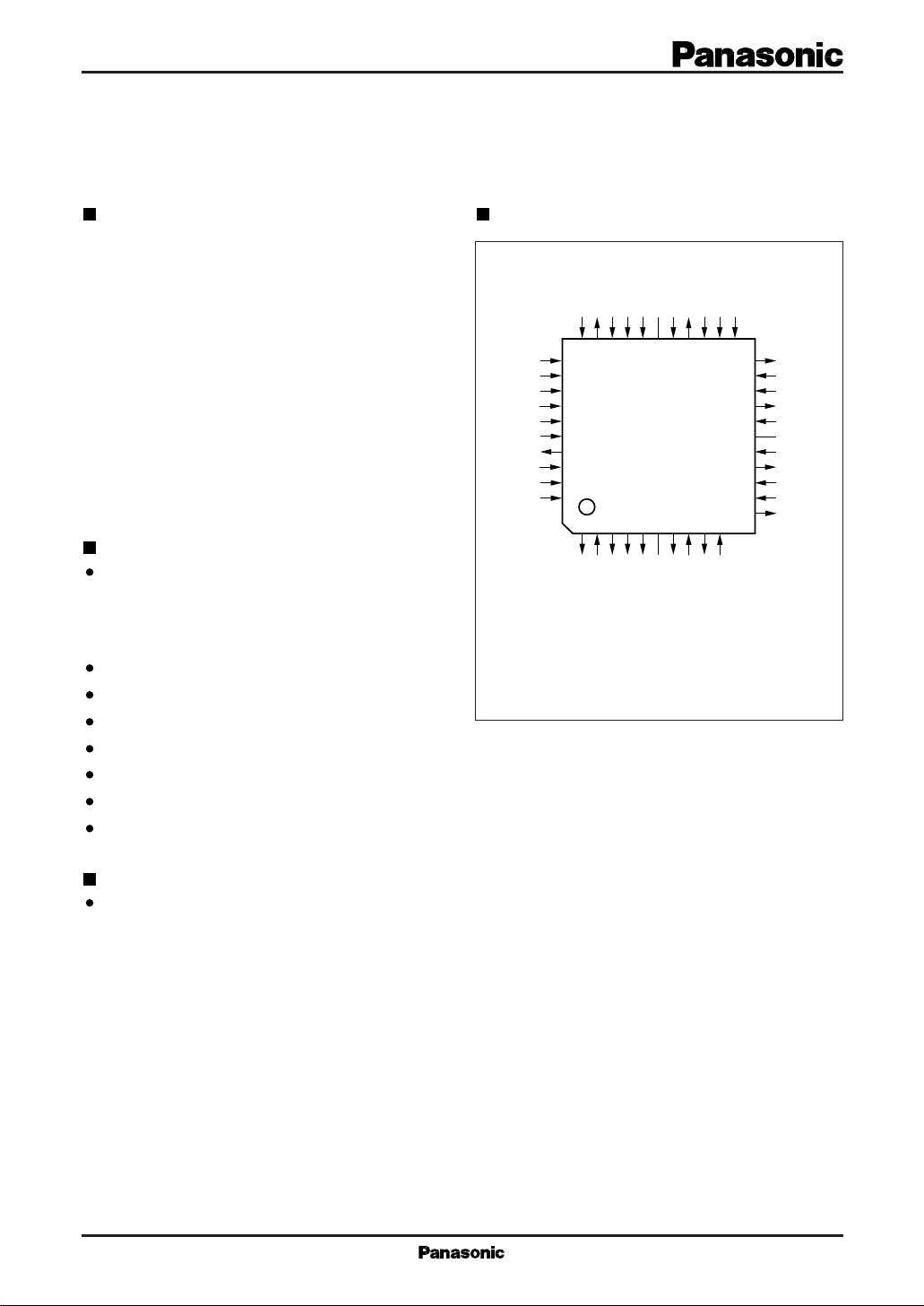
Pin Assignment
192FS
ZFLGB
3231302928272625242322
SS3
PD
33
34
35
36
37
38
DD
39
40
41
42
123456789
MLD
RSTB
QFP042-P-1414A
LRPOL
LRCLK
BCLK
SRDATA
DV
DV
384FS
MDATA
MCLK
SS2DVDD2
NSUB
DV
N.C.X1X2
IE
TP1
TP2
TEST1
TEST2
(TOP VIEW)
N.C.
SS1DVDD1AVDD1
DV
10
DD4
N.C.
AV
21
OUTR(–)
20
AV
19
18
17
16
15
14
13
12
11
SS1
AV
SS2
OUTR(+)
AV
DD2
N.C.
AV
DD3
OUTL(+)
AV
SS3
AV
SS4
OUTL(–)
Applications
CD players and other digital audio equipment
Page 2
MN6474A For Audio Equipment
Block Diagram
LRPOL
LRCLK
BCLK
SRDATA
Analog
Block
(R)
Analog
Block
(L)
X2
25
21
18
14
11
OUTR
OUTR
OUTL
OUTL
(–)
(+)
(+)
(–)
ZFLGB
TP1
TP2
TEST1
TEST2
7
6
5
4
31
33
34
S/P
35
Converter
36
3
IE
Microcomputer Interface
FIR 1 FIR 2
40PD41
42
1
384FS
39
Timing Generator
Noise
Shaping
Logics
192FS
32
X1
26
PWM
Logics
(R)
PWM
Logics
(L)
MCLK
MDATA
MLD
Page 3

For Audio Equipment MN6474A
Pin Descriptions
Pin No. Symbol Function Description
1 MLD Microcomputer command load input ("L" level to load)
2 RSTB Reset pin (active "L").
Always pull this pin low after applying the power.
2
3 IE Input format selection pin. "H" level; I
"L" level; signal processing LSI format.
4 TP1 Digital filter test output pin 1. Leave this pin open.
5 TP2 Digital filter test output pin 2. Leave this pin open.
6 TEST1 Digital filter test input pin 1. Keep this pin at "L" level.
7 TEST2 Digital filter test input pin 2. Keep this pin at "L" level.
8 N.C. No connection Leave these pins open.
9 N.C. No connection Leave these pins open.
10 AV
DD4
Power supply pin 4 for analog circuits. (+5V)
11 OUTL(–) Left channel inverted phase PWM output pin.
12 AV
13 AV
SS4
SS3
Ground pin 4 for analog circuits.
Ground pin 3 for analog circuits.
14 OUTL(+) Left channel normal phase PWM output pin.
15 AV
DD3
Power supply pin 3 for analog circuits. (+5V)
16 N.C. No connection Leave this pin open.
17 AV
DD2
Power supply pin 2 for analog circuits. (+5V)
18 OUTR(+) Right channel through phase PWM output pin.
19 AV
20 AV
SS2
SS1
Ground pin 2 for analog circuits.
Ground pin 1 for analog circuits.
21 OUTR(–) Right channel inverted phase PWM output pin.
22 AV
23 DV
24 DV
DD1
DD1
SS1
Power supply pin 1 for analog circuits. (+5V)
Power supply pin 1 for digital circuits. (+5V) (Power supply for oscillator circuit)
Ground pin 1 for digital circuits. (Ground for oscillator circuit)
25 X2 Crystal oscillator pin.
26 X1 Crystal oscillator pin. (External clock input pin)
27 N.C. No connection Leave this pin open.
28 DV
29 DV
DD2
SS2
Power supply pin 2 for analog circuits. (+5V)
Ground pin 2 for digital circuits.
30 NSUB Connect to D-VDD. (Silicon substrate potential fixing pin)
31 ZFLGB Output pin for detecting zero input.
32 192FS 192fs(=9.216 MHz)output pin. Max. load capacity: 30 pF.
33 LRPOL LRCLK polarity selection pin. "H" level; selects the left channel
"L" level; the right channel.
34 LRCLK LRCLK pin. When the LRPOL pin is at "H" level, "H" level in this pin indicates left
channel data input; "L" level indicates right channel data input. When the LRPOL pin
is at "L" level, "L" level in this pin indicates left channel data input; "H" level input
indicates right channel data input.
35 BCLK Serial input bit clock
36 SRDATA Serial input data (digital) input pin.
37 DV
SS3
Ground pin 3 for digital circuits.
S format
Page 4

MN6474A For Audio Equipment
Pin Descriptions (continued)
Pin No. Symbol Function Description
38 DV
DD
39 384FS 384fs (=18.432 MHz) output pin. Max. load capacitance: 30 pF.
40 PD Power down pin. (active "H")
41 MDATA Microcomputer command data input pin.
42 MCLK Clock input pin for microcomputer command.
Conversion Characteristics
DVDD=5.0V, DVSS=0V, AVDD=5.0V, AVSS=0V, f=33.8688MHz, Ta=25˚C
Parameter Symbol Test Conditions min typ max Unit
Analog characteristics
Signal-to-noise ratio S/N EIAJ (1kHz) 95 106 dB
Dynamic range D.R. EIAJ (1kHz) 90 98 dB
Total harmonic distortion THD+N EIAJ (1kHz) 0.003 0.005 %
Crosstalk EIAJ (1kHz) 90 98 dB
Output level *
Note*1: These analog characteristics are for circuits equivalent to the suggested application circuit.
1
Power supply pin for digital circuits. (Silicon substrate potential fixing pin.) (+5V)
1kHz F.S. 1.4 1.7 V
rms
Page 5

For Audio Equipment MN6474A
Application Circuit Example
R30
100kW
R29
2345678910
7th order L.P.F(HAF 0079)
1
R8 1kW
R7 1kW
R6 1kW
–15 E 15
R5 1kW
R23
22W
C28
220µF
+
N
C26 2200pF
R19
220W
R17
C22
47pF
C13
22µF
++
C12
22µF
++
C11
22µF
C10
22µF
R34
470kW
10µF
47kW
R13
R ch
R27
C24
33kW
330W
N
C32
C29
R24
100kW
C34
330pF
10µF
220µF
+
22W
+–8
+–8
+
IC4
C35
330pF
R26
22W
1–+
1–+
C31
IC2
220µF
L ch
R28
330W
N
C33
10µF
C27 2200pF
C20 47pF
R21
33kW
R14
47pF
C23
47kW
R35
R20
470kW
N
220W
R15
10µF
47kW
R18
33kW
C32
+
C25
R25
220µF
22W
2345678910
7th order L.P.F(HAF 0079)
1
IC3
+–8
1–+
IC1
+–8
1–+
C21
47pF
R16
R22
33kW
47kW
IC1 to 4
AN6558
SS
AV
R3 330W
DD
AV
DD
DV
SS
DV
R4 330W
+
*C1
100µF
R1
10W
+
C14 47µF
C15 47µF
*C5 10µF
5pF
C4
C3 5pF
R32
+
R2
33.8688
MHz
470W
*C6 0.56µF
4.7kW
47pF
47pF
C16
C17
R9
47kW
R10
C7
47kW
+
R11
330µF
16
17
18
19
20
21
(–)
(+)
SS2AVSS1
DD2
N.C.
AV
OUTR
22
AV
DD1
23
DV
+
DD1
24
DV
SS1
25
X2
26
X1
27
N.C.
28
DV
DD2
29
DV
SS2
30
NSUB
31
ZFLGB
32
192f
s
AV
OUTR
MN6474A
LRCLK
BCLK
SS3DVDD
SRDATA
DV
+
LRPOL
333435363738394041
C2
R32
470W
470W
C18
47pF
47kW
+
C8
330µF
13
14
15
(+)
DD3
AV
OUTL
384FSPDMDATA
100µF
R33
47pF
C19
12
SS4AVSS3
AV
R12
47kW
11
OUTL(–)
AV
DD4
N.C.
N.C.
TEST2
TEST1
TP2
TP1
IE
RSTB
MLD
MCLK
42
*C9
0.56µF
10
9
8
7
6
5
4
3
2
1
VDDVSS*C1,C5,C6 and C9 are attached to the rear of the P base.
S2 S3 S1 S4 S5 S6
)
S4
(
IE
Signal processing
)
S1
(
Reset
RSTB
)
S3
(
–
PD
"L"
S format
2
LSI format
I
–
Power
"H"
down mode
Page 6

MN6474A For Audio Equipment
Package Dmensions (Unit: mm)
QFP042-P-1414A
18.7±0.4
14.0±0.2
32 22
21
33
(0.65)
14.0±0.2
18.7±0.4
42
(1.92)
11
110
1.27
0.4
±0.1
±0.20.1±0.1
2.2
2.6max.
+0.10
0.05
-
0.15
0.15
SEATING PLANE
(2.35)
(1.5±0.2)
0 to 10°
 Loading...