

Page 1
CCD Delay Line Series
MN3885S
NTSC-Compatible CCD Video Signal Delay Element
Overview
The MN3885S is a CCD signal delay element for video
signal processing applications.
It contains such components as a shift register clock
driver, charge I/O blocks, two CCD delay elements, a
clamp bias circuit, resampling output amplifiers, and
booster circuits.
The MN3885S samples the input using the supplied
clock signal with a frequency 7.15909 MHz of twice the
NTSC color signal subcarrier frequency, and after adding in the attached filter delay, produces independent delays of 1 H (the horizontal scan period) each for the two
lines.
Features
Single 5.0 V power supply
Single chip combining luminance signal delay line and
delay line for color signal converted to the low frequency.
Low EMI levels from clock during driving
Applications
VCRs, Video cameras
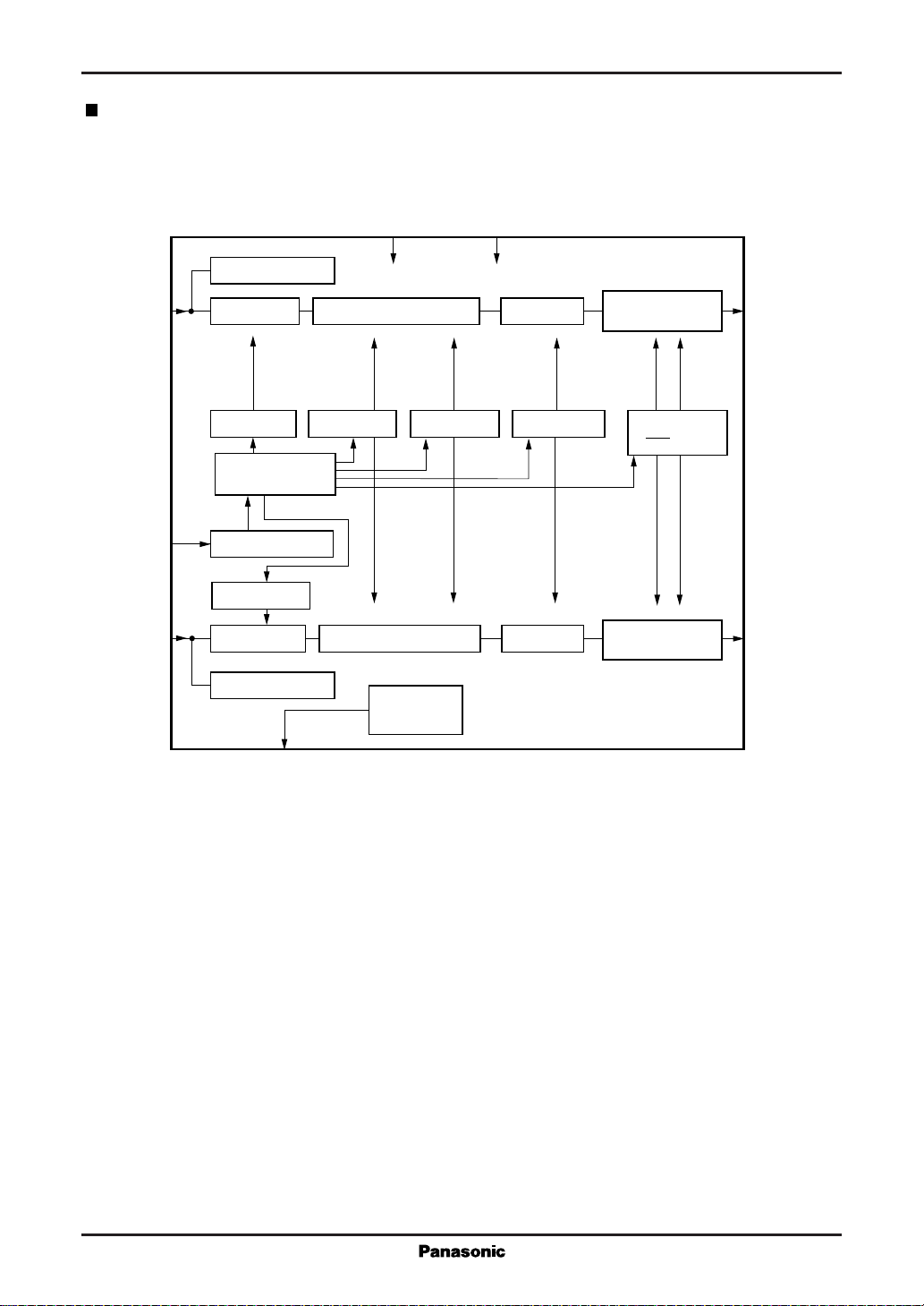
Structure and Operation
The MN3885S consists of the operational blocks shown
in the block diagram. The shift register has the structure
shown in the supplementary diagram.
Shift register clock driver
This block generates two transfer clock signals, ø1 and
ø2, synchronized with the 7.15909 MHz input clock signal.
It also generates the sampling clock signals øS and øS',
resampling clock signal øSH, and reset clock signal øR
based on the timing control.
Charge Input blocks
These blocks alter the analog input signals from the
VINC and VINY pins on their way to the shift registers.
One adds the bias voltage specified with the bias circuit
to the analog signal from the VINC pin. The other applies an "L" level clamp voltage from the clamp circuit
to the analog signal from the VINY pin.
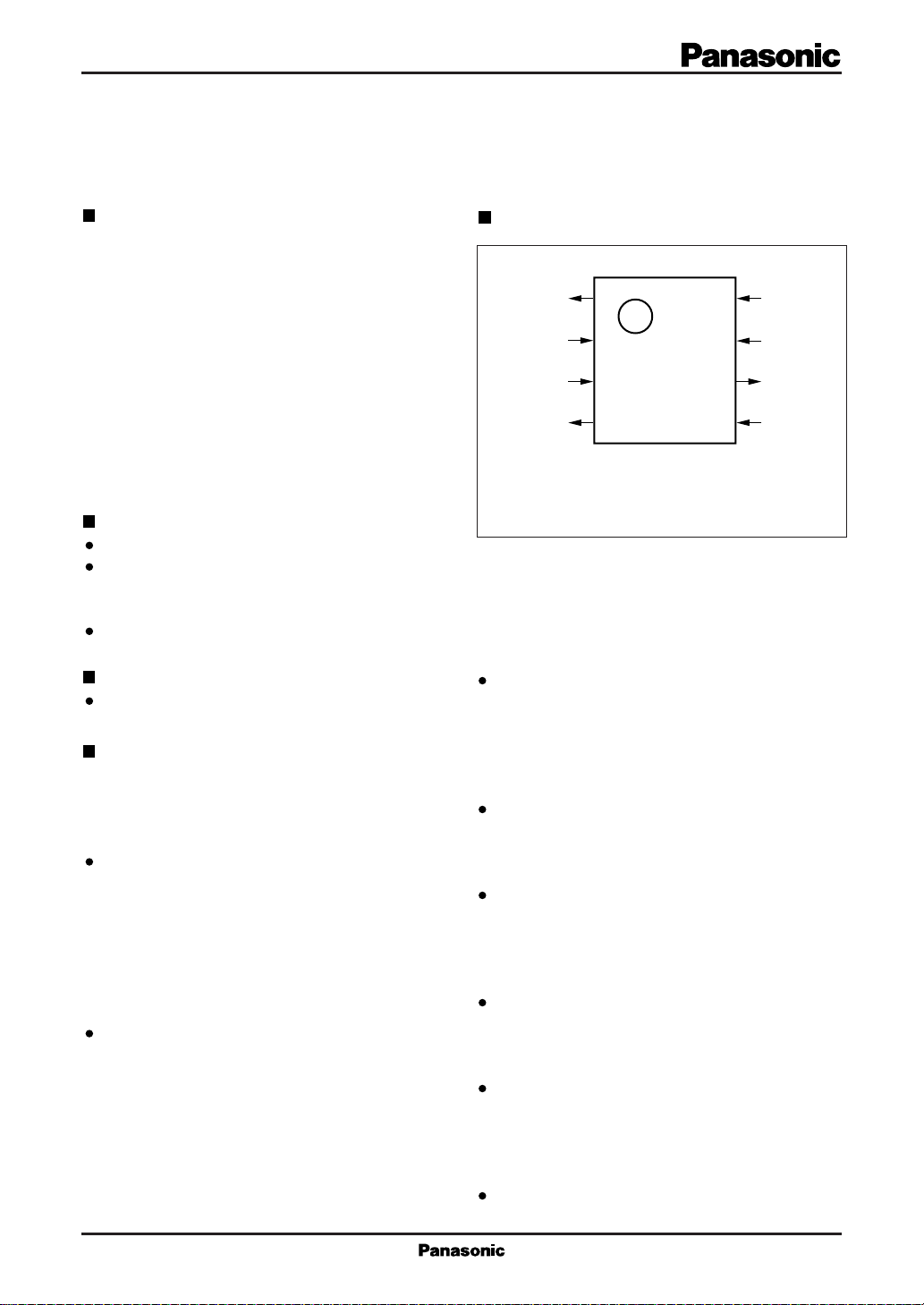
Pin Assignment
VOC
V
V
VOY
Analog shift registers
These blocks sample the shift register input signals with
the sampling clock, and convert the results to charges,
and use transfer clocks ø1 and ø2 to transfer the results to
the following block.
Charge detection blocks
These convert the signal charges from the final stage
of the analog shift registers into voltage signals.
Resampling output amplifiers
In the output stage of this blocks, the voltage signal is
executed Sample-and-Hold by resampling, and is outputted at signal output pin of VOC (1-pin) and V OY (4-pin).
Bias circuit
This circuit applies a bias voltage to the analog signal
from VINC (pin 8) to optimize it for the shift register.
Clamp circuit
This circuit applies an "L" level clamp to the analog
signal from VINY (pin 5) to optimize it for the shift register.
1
2
DD
3
SS
4
SOP008-P-0225A
( TOP VIEW )
8
VINC
7
XI
6
V
BB
5
VINY
Booster circuits
These generate reset drain voltages.
1
Page 2
MN3885S CCD Delay Line Series
Block Diagram
VINC
XI
VINY
8
Charge input
block
øS driver
Timing adjustment
7
Waveform amplifier
adjustment block
øS' driver
5
Charge input
block
Clamp circuit
Bias circuit
6
3
CCD 454 stages
ø1 driver
CCD 453.5 stages
Substrate bias
generator
V
SS
ø2 driver
DD
V
2
Charge
detection block
øR driver
Charge
detection block
Resampling
output amplifier
øSH driver
øSH driver
Resampling
output amplifier
1
VOC
4
VOY
BB
V
2
Page 3

CCD Delay Line Series MN3885S
Pin Descriptions
Pin No. Symbol Pin Name Remarks
1 VOC Signal output (C)
2VDDPower supply
3VSSGround
4 VOY Signal output (Y)
5 VINY Signal input (Y)
6VBBSubstrate connection Negative voltage pin
7 XI Clock input
8 VINC Signal input (C)
Operating Conditions
Parameter Symbol min typ max Unit
Power supply V
Input clock frequency f
Input clock amplitude (sine wave) v
DD
ck
ck
Ambient temperature Ta –20 60 ˚C
Electrical Characteristics
VDD=5.0V, Vck=0.3V
Parameter Symbol Conditions min typ max Unit
Power supply voltage I
Signal bandwidth (Y signal) BWY –3 dB for 200 kHz value 1.8 2.8
Signal bandwidth (C signal) BWC –3 dB for 200 kHz value 1.8 2.8
Insertion gain (Y signal) IGY f
Insertion gain (C signal) IGC f
Total harmonic distortion THD f
Signal-to-noise ratio S/N Signal output (V
Clock leak NC 7.16 MHz components for both
Crosstalk CT f
Delay (Y signal) τ
Delay (C signal) τ
VO pin output impedance Z
Input bias voltage V
Input clamp voltage V
Output bias voltage V
Output clamp voltage V
Substrate voltage –V
(sine wave), Vin=0.5V
P-P
(sine wave), fck=7.15909MHz, Ta=25˚C
P-P
DD
=200kHz 0.0 3.0 6.0
sig
=200kHz –1.0 2.0 5.0
sig
=200kHz 1.0 4.5 %
sig
Y and C signals
=200kHz –50 –35 dB
sig
DY
DC
OY
Z
OC
Applied to input from C signal input pin 2.86 V
BIN
Applied to input from Y signal input pin 2.70 V
CLIN
Applied to output from C signal output pin 2.70 V
BO
Applied to output from Y signal output pin 2.40 V
CLO
BB
4.75 5.00 5.25 V
7.15909 MHz
0.2 0.3 1.5 V
18 36 mA
)/noise output (rms) 48 56 dB
p-p
–30 –10 dB
63.38
63.46
0.5 0.9
0.5 0.9
–2.80 V
P–P
MHz
dB
µs
kΩ
3
Page 4

MN3885S CCD Delay Line Series
VINY Shift Register Configuration
VINY
Clamp circuit
øS' ø1 ø2
øR
Booster
circuit
Voltage
generator
2
V
DD
.......
.......
øSH
5
Output
amplifier
4
VOY
3
V
SS
4
Page 5

CCD Delay Line Series MN3885S
Application Circuit Example
10µF
–
+
0.1µF
VINC
0.01µF
8
Bias circuit
Charge input
block
SS
V
3
CCD 454 stages
DD
V
2
Charge
detection block
Resampling
output amplifier
330Ω
1
VOC
2SA564
øS driver ø1 driver ø2 driver øR driver
øSH driver
øSH driver
Timing adjustment
XI 7
1000pF
Waveform amplifier
adjustment block
øS' driver
VINY
0.47µF
5
Charge input
block
CCD 453.5 stages
Charge
detection block
Resampling
output amplifier
Clamp circuit
Substrate bias
generator
6
BB
V
0.01µF
Note: If the external capacitor attached to pin 6 is a electrolytic capacitor, connect the negative pole to pin 6.
330Ω
4
VOY
2SA564
5
Page 6

MN3885S CCD Delay Line Series
Package Dimensions (Unit:mm)
SOP008-P-0225A
0.4±0.25
0.4
1.27
1
4
8
5.0±0.3
5
0.1±0.1
0.3
4.2±0.3
6.5±0.3
0.15
1.5±0.2
0.65
6
 Loading...