

Page 1
CCD Delay Line Series
MN3867S
PAL-Compatible CCD Video Signal Delay Element
Overview
The MN3867S is a CCD signal delay element for video
signal processing applications.
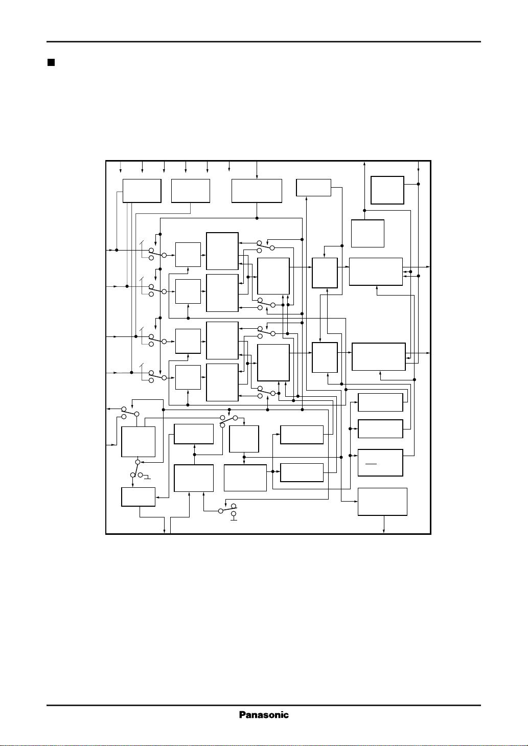
It contains such components as a threefold-frequency
circuit, a shift register clock driver, charge I/O blocks,
two CCD analog shift registers switchable between 1700
and 617 stages and between 848.5 and 617 stages, a clamp
bias circuit, resampling output amplifiers, and booster
circuits.
When the switch input is "L" level, the MN38667S
samples the input using the supplied clock signal with a
frequency three times the PAL color signal subcarrier frequency (4.43361875 MHz) and, after adding in the attached filter delay, produces independent delays of 1 H
(the horizontal scan period) and 2 H for the two lines.
When the switch input is "H" level, the MN38667S disables the threefold-frequency circuit and samples the input with the image sensor drive frequency (9.65625 MHz)
for the camera's 510 horizontal pixels and, after adding
in the attached filter delay, produces independent delays
of 1 H (the horizontal scan period) each for the two lines.
Features
Single 5.0 V power supply
Choice of camera and VCR modes, so that both the
camera and VCR portions of a video camera with 510
horizontal pixels can use the same MN38667S for signal processing
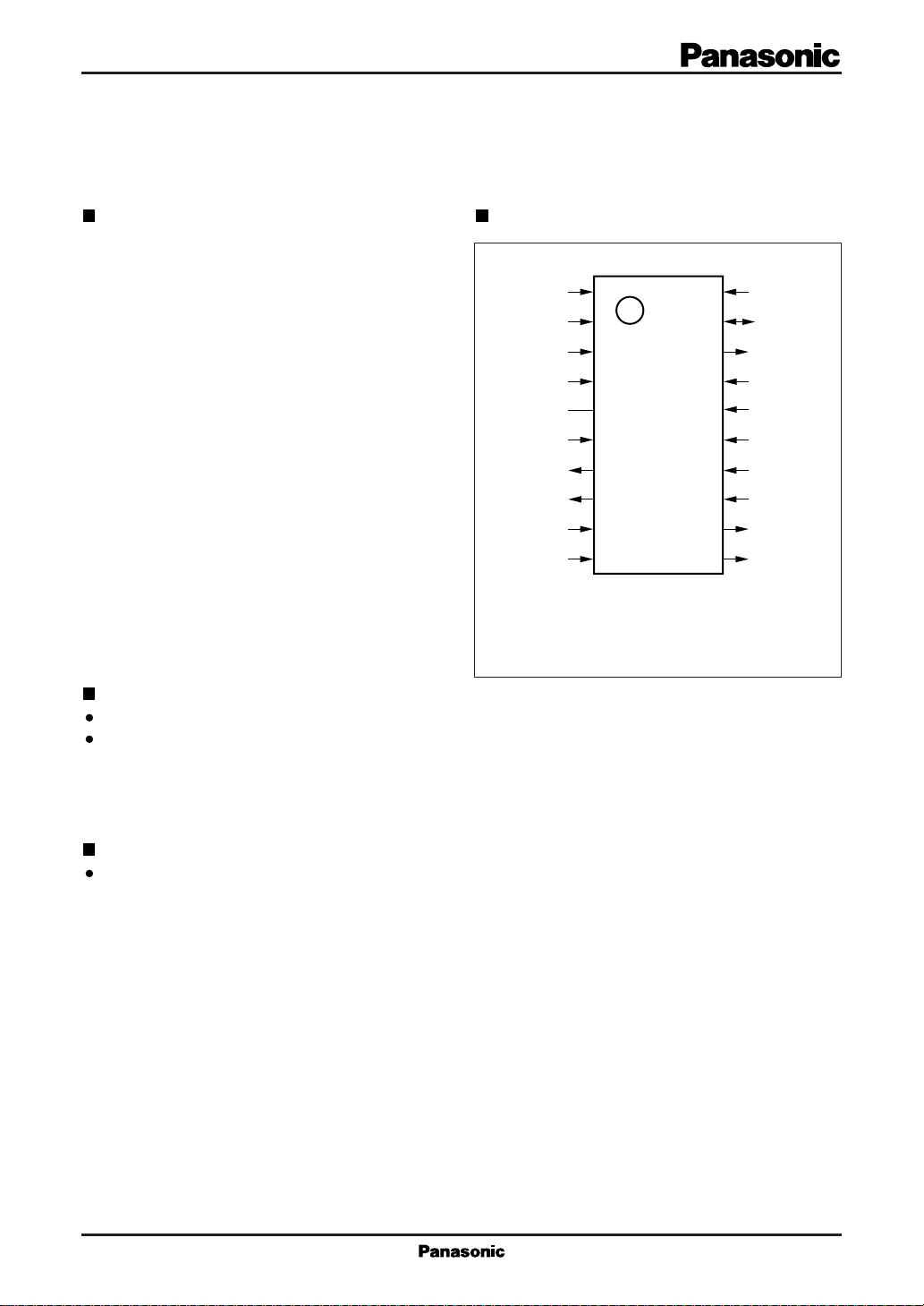
Pin Assignment
XIC
V
SS3
V
DD3
VINC1
N.C.
VINVC
VGC1
VO1C
V
DD1
V
SS1
1
2
3
4
5
6
7
8
9
10
SOP020-P-0300C
( TOP VIEW )
20
19
18
17
16
15
14
13
12
11
XIV
PCOUT
&
VCOIN
–V
BB
V
SS2
V
DD2
VINVY
SW
VINC2
VGC2
VO2Y
Applications
Video cameras
1
Page 2
MN3867S CCD Delay Line Series
Block Diagram
DD1VSS1VDD2VSS2VDD3VSS3
VINVC
VINC1
VINVY
VINC2
XIV
XIC
6
4
15
13
20
1
V
9
Bias circuit
L
H
Waveform
amplifier
adjustment
block
L
Phase
comparator
3
10
16
17
2
Clamp
circuit
Charge
input
block
Charge
input
block
Charge
input
block
Charge
input
block
1086-stage
analog
shift
register
3-stage
analog
shift
register
234.5-stage
analog
shift
register
3-stage
analog
shift
register
L
H
H
L
L
H
H
L
H
1/3rd
frequency
divider
H
VCO
L
Timing
adjustment
19
Mode switch
L
H
L
H
L
H
L
H
Waveform
adjustment
block
L
H
SW
14
614-stage
analog
shift
register
614-stage
analog
shift
register
Booster
circuit
ø1 driver
ø2 driver
Charge
detector
Charge
detector
VGC1
7
Voltage
generator
Voltage
generator
Resampling
output amplifier
Resampling
output amplifier
øS driver
øR driver
øSH driver
øSH driver
Substrate bias
generator
18
BB
–V
VGC2
12
11
8
VO1C
VO2Y
PCOUT & VCOIN
2
Page 3
CCD Delay Line Series MN3867S
Pin Descriptions
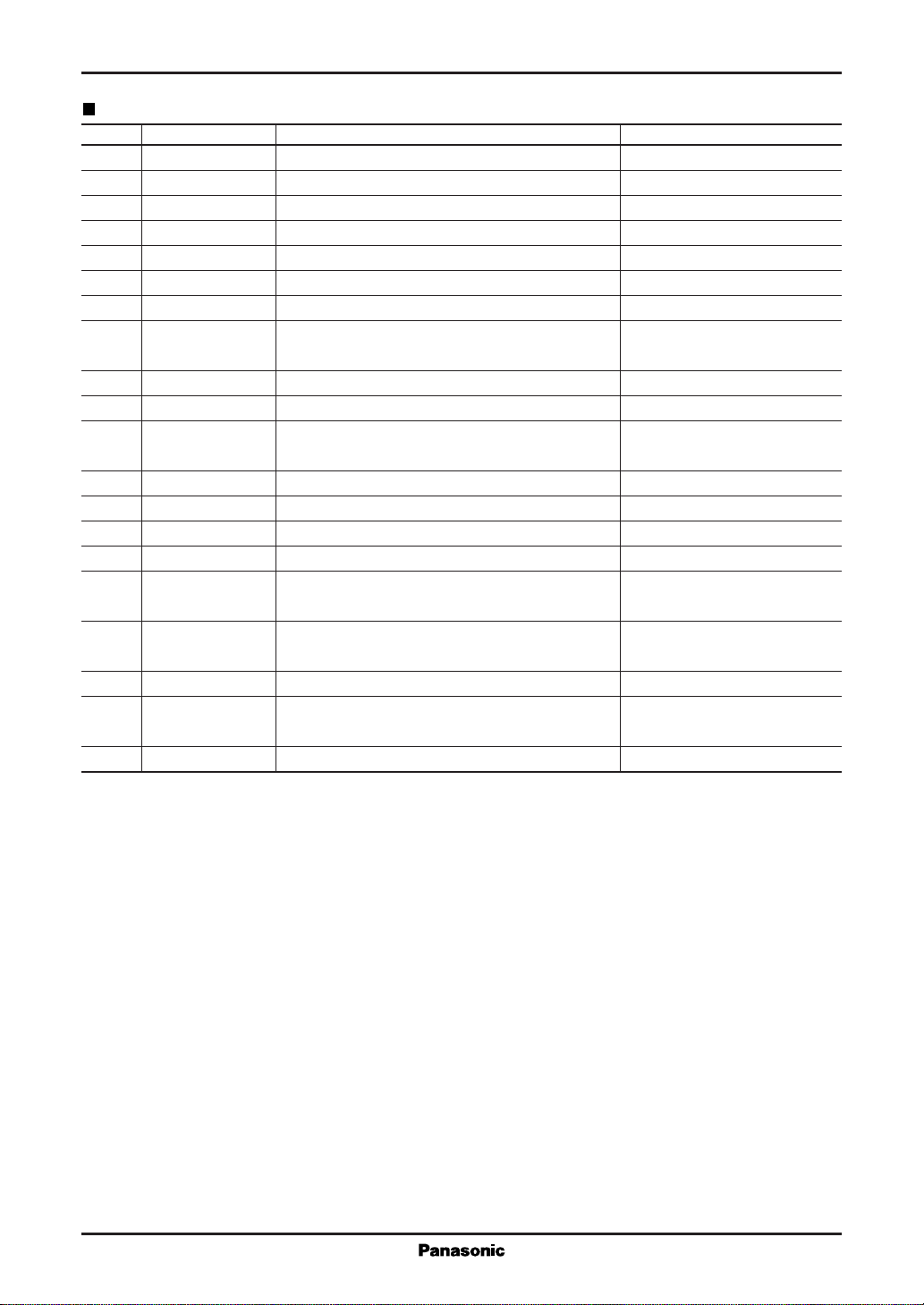
Pin No. Symbol Pin Name Remarks
1 XIC 9.65625 MHz clock input
2V
3V
SS3
DD3
4 VINC1 Camera signal input (1)
5 N.C. No connection
6 VINVC Video signal input (C)
7 VGC1 Output gate connection (1)
8 VO1C Signal output (1C) Output pin for signal
9V
10 V
DD1
SS1
11 VO2Y Signal output (2Y) Output pin for signal
12 VGC2 Output gate connection (2)
13 VINC2 Camera signal input (2)
14 SW Camera/video mode switch
15 VINVY Video signal input (Y)
16 V
17 V
18 –V
DD2
SS2
BB
19 PCOUT&VCOIN Phase comparator output and voltage controlled
20 XIV 4.43361875 MHz clock input
Notes
1: Always connect V
2: Always connect V
DD1
SS1
, V
, V
GND (3) Ground for clock multiplier circuit
Power supply (3) Power supply for clock multiplier circuit
fed to pin 4 or pin 6
Power supply (1) Power supply for analog circuits
GND (1) Ground for analog circuits
fed to pin 13 or pin 15
Power supply (2) Power supply for digital circuits
other than frequency multiplier
GND (2) Ground for digital circuits
other than frequency multiplier
Substrate connection Negative voltage pin
oscillator input
DD2
SS2
, and V
, and V
to the same voltage.
DD3
to ground.
SS3
3
Page 4
MN3867S CCD Delay Line Series
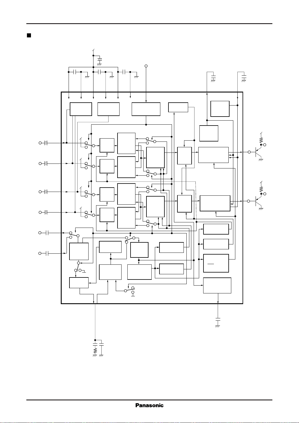
Application Circuit Example
+
5.0V
10µF
–
0.1µF
DD1VSS1VDD2VSS2VDD3VSS3
V
9
Bias circuit
10
16
0.1µF 0.1µF
3
17
Clamp
circuit
2
5.0V or GND
SW
14
Mode switch
Booster
circuit
0.01µF
VGC1
7
0.01µF
VGC2
12
Voltage
generator
Signal
input
–
0.47µF
Signal
input
–
0.47µF
Signal
input
–
0.47µF
Signal
input
–
0.47µF
Clock
input
1000pF
Clock
input
1000pF
VINVC
+
VINC1
+
VINVY
+
VINC2
+
XIV
XIC
6
4
15
13
20
1
L
H
Waveform
amplifier
adjustment
block
L
H
Phase
comparator
Voltage
L
Charge
input
block
H
H
Charge
input
block
L
L
Charge
input
block
H
H
Charge
input
block
L
1086-stage
analog
shift
register
3-stage
analog
shift
register
234.5-stage
analog
shift
register
3-stage
analog
shift
register
L
H
614-stage
analog
shift
register
L
H
L
H
614-stage
analog
shift
register
L
H
Charge
detector
Charge
detector
generator
Resampling
output amplifier
Resampling
output amplifier
øS driver
8
11
VO1C
Signal
output
(1C)
VO2Y
Signal
output
(2Y)
H
1/3rd
frequency
divider
L
Waveform
adjustment
block
ø1 driver
øR driver
øSH driver
øSH driver
VCO
Timing
adjustment
ø2 driver
Substrate bias
L
generator
H
19
18
BB
–V
0.01µF
PCOUT & VCOIN
0.01µF 1000pF
820Ω
Note: If the capacitor attached to pin 18 has a polarity, attach the negative pole to pin 18.
4
Page 5
CCD Delay Line Series MN3867S
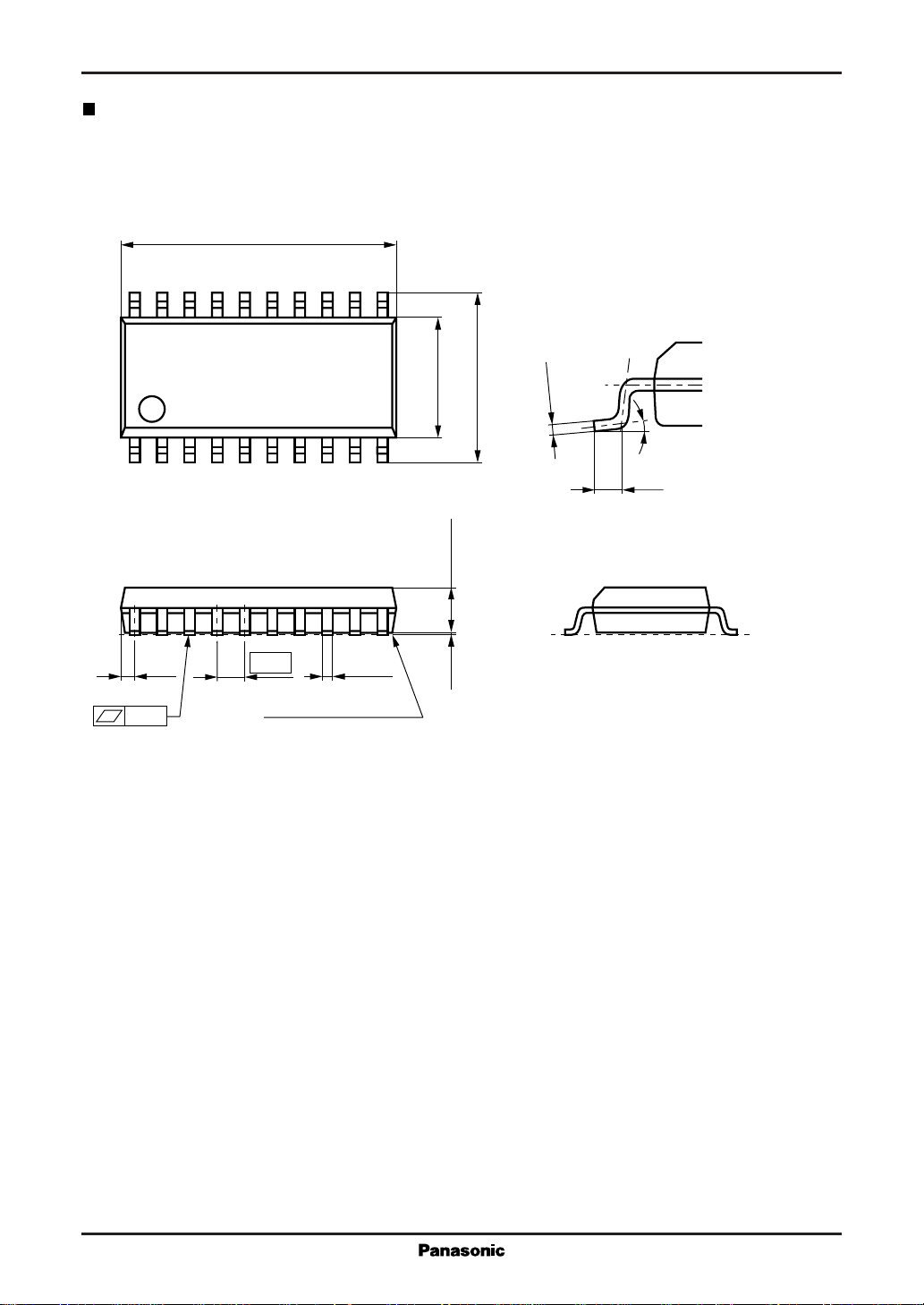
Package Dimensions (Unit:mm)
SOP020-P-0300C
12.63
±0.3
20
1
(0.6)
0.10
11
10
1.27
0.4±0.25
SEATING PLANE
5.5±0.3
2.05±0.2
0.1±0.1
7.6±0.3
0.05
-
+0.10
0.2
0 to 10°
(0.4)
5
Page 6

 Loading...