

Page 1

CCD Delay Line Series
MN3870S
NTSC-Compatible CCD Comb Filter with Built-in 1 H Video Signal Dela y Element
Overview
The MN3870S is a 4 fSC CMOS CCD comb filter with
a built-in 4 f
CMOS CCD signal delay element for video
SC
signal processing applications.
It contains such components as a fourfold-frequency
circuit, a shift register clock driver, a CCD analog shift
register switchable between 911, 1 and 908 / 906 stages,
and a resampling output amplifier.
It samples the input using the supplied clock signal with
a frequency of four times the color signal subcarrier frequency (3.58 MHz) and subtracts between the 911- and
1-stage CCD output signals to produce the color signal
comb characteristics for the NTSC system.
It also uses this fourfold frequency to drive a 908- or
906-stage CCD and samples the input to produce, after
adding in the attached filter delay, a delay of 1 H (the
horizontal scan period) when the SW pin is left open.
Features
Single 5.0 V power supply
Low power consumption based on CMOS process
Low EMI levels from clock during driving
True comb filter produced by the subtraction of the
through signal and the 1 H delay signal
Pin Assignment
X1
V
BB
N.C.
VGC1
VOC
VINC
N.C.
N.C.
V
SS1
V
DD1
1
2
3
4
5
6
7
8
9
10
SOP020-P-0300C
( TOP VIEW )
PCOUT
20
19
18
17
16
15
14
13
12
11
&
VCOIN
N.C.
V
SS3
V
DD3
V
DD2
V
SS2
VGC2
SW
VINY
VOY
Applications
VCRs, Video cameras
1
Page 2
MN3870S CCD Delay Line Series
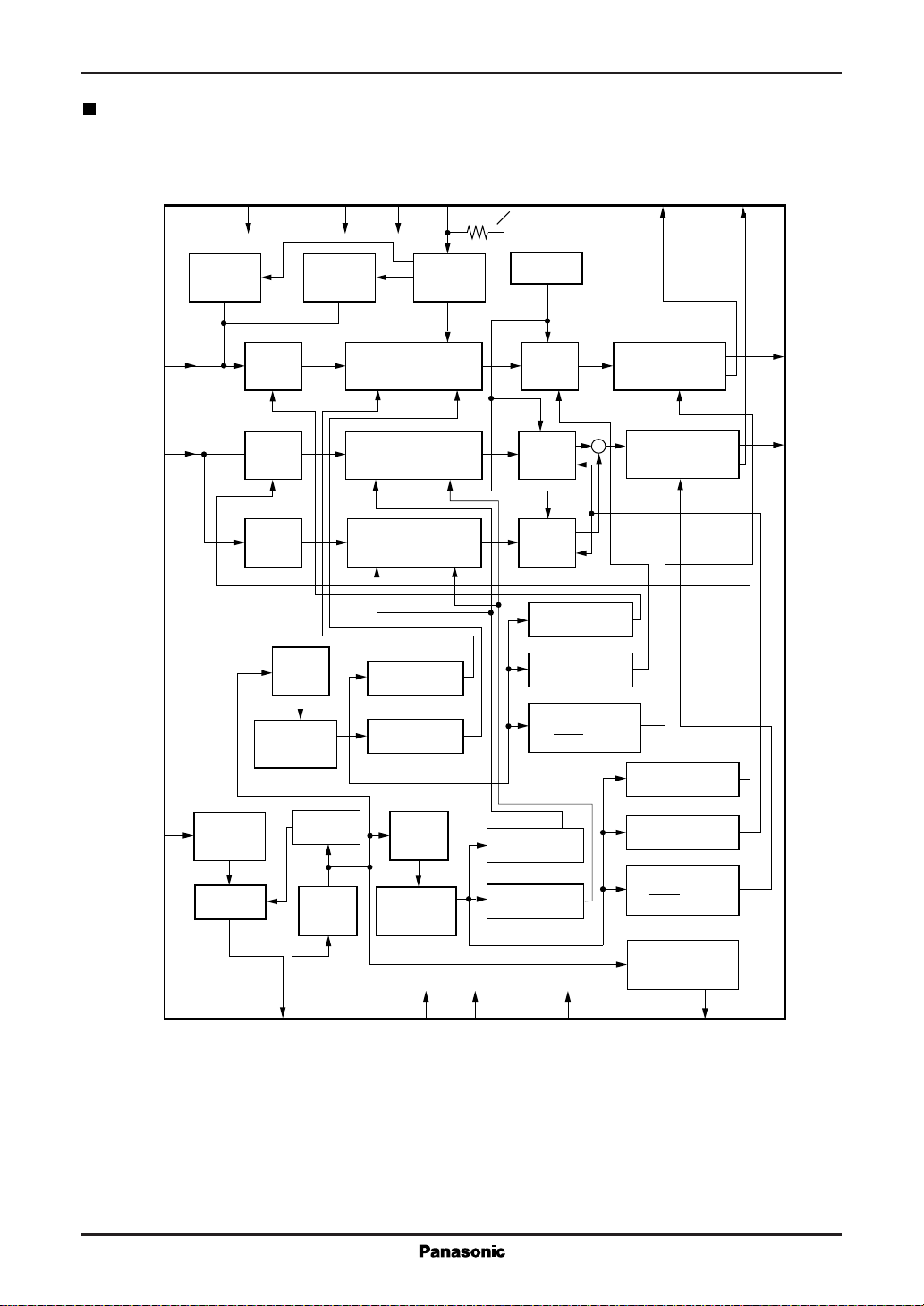
Block Diagram
VINY
VINC
DD1
V
10
Clamp
circuit
12
Charge
input
block
6
Charge
input
block
Charge
input
block
DD2VDD3
V
16
Bias circuit
908 or 906-stage
analog shift register
911-stage
analog shift register
1-stage
analog shift register
SW
17
13
Mode
switch
Booster
circuit
Charge
detector
Charge
–
detector
VGC1
4
Resampling
output amplifier
Resampling
output amplifier
VGC2
14
11
VOY
5
VOC
Charge
detector
øSY driver
Waveform
adjustment
block
ø1Y driver
øRY driver
XI
1
Waveform
amplifier
adjustment
block
Phase
comparator
Timing
adjustment
1/4th
frequency
divider
VCO
20
PCOUT & VCOIN
ø2Y driver
Waveform
adjustment
block
Timing
adjustment
9
SS1VSS2
V
15
øSHY driver
øSHY driver
ø1C driver
ø2C driver
øSC driver
øRC driver
øSHC driver
øSHC driver
Substrate bias
generator
18
SS3
V
2
BB
V
2
Page 3
CCD Delay Line Series MN3870S
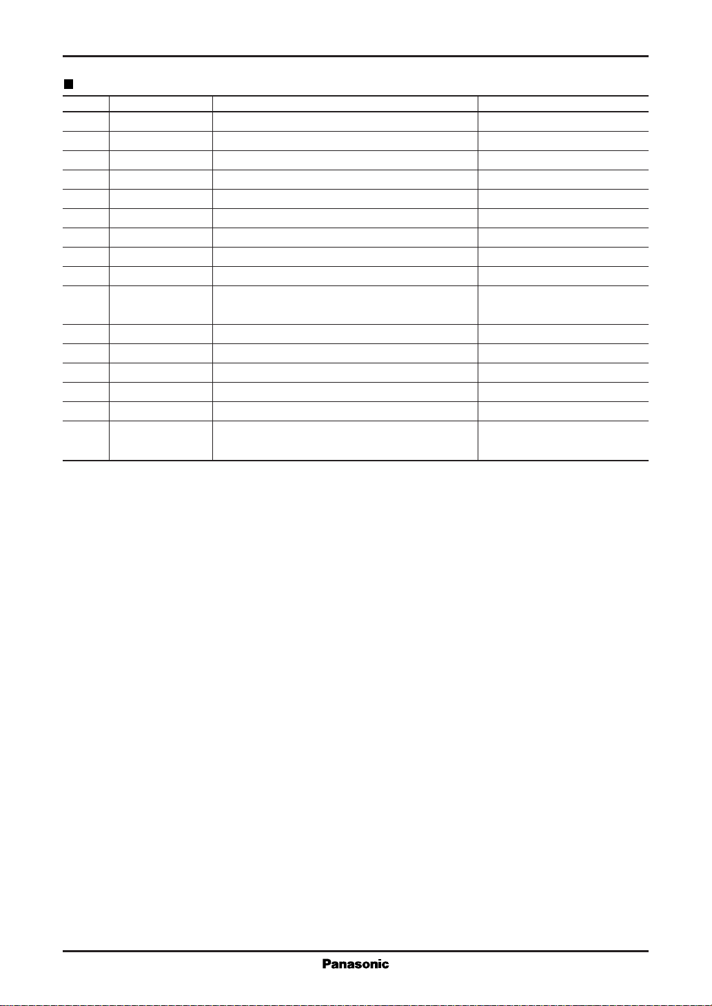
Pin Descriptions
Pin No. Symbol Pin Name Remarks
1 XI 3.58 MHz clock input
2VBBSubstrate connection
4 VGC1 Output gate connection (1)
5 VOC C signal output
6 VINC C signal input
9V
10 V
SS1
DD1
11 VOY Y signal output
12 VINY Y signal input
13 SW Switch controlling number of stages for Y signal
14 VGC2 Output gate connection (2)
15 V
16 V
17 V
18 V
SS2
DD2
DD3
SS3
20 PCOUT Phase comparator output and voltage controlled
&VCOIN oscillator input
Note: Leave pin 13 open.
GND (1) Ground for analog circuits
Power supply (1) For analog circuits
delay
GND (2) Ground for digital signals
Power supply (2) For digital signals
Power supply (3) For phase-locked loop
GND (3) Ground for phase-locked loop
3
Page 4
MN3870S CCD Delay Line Series
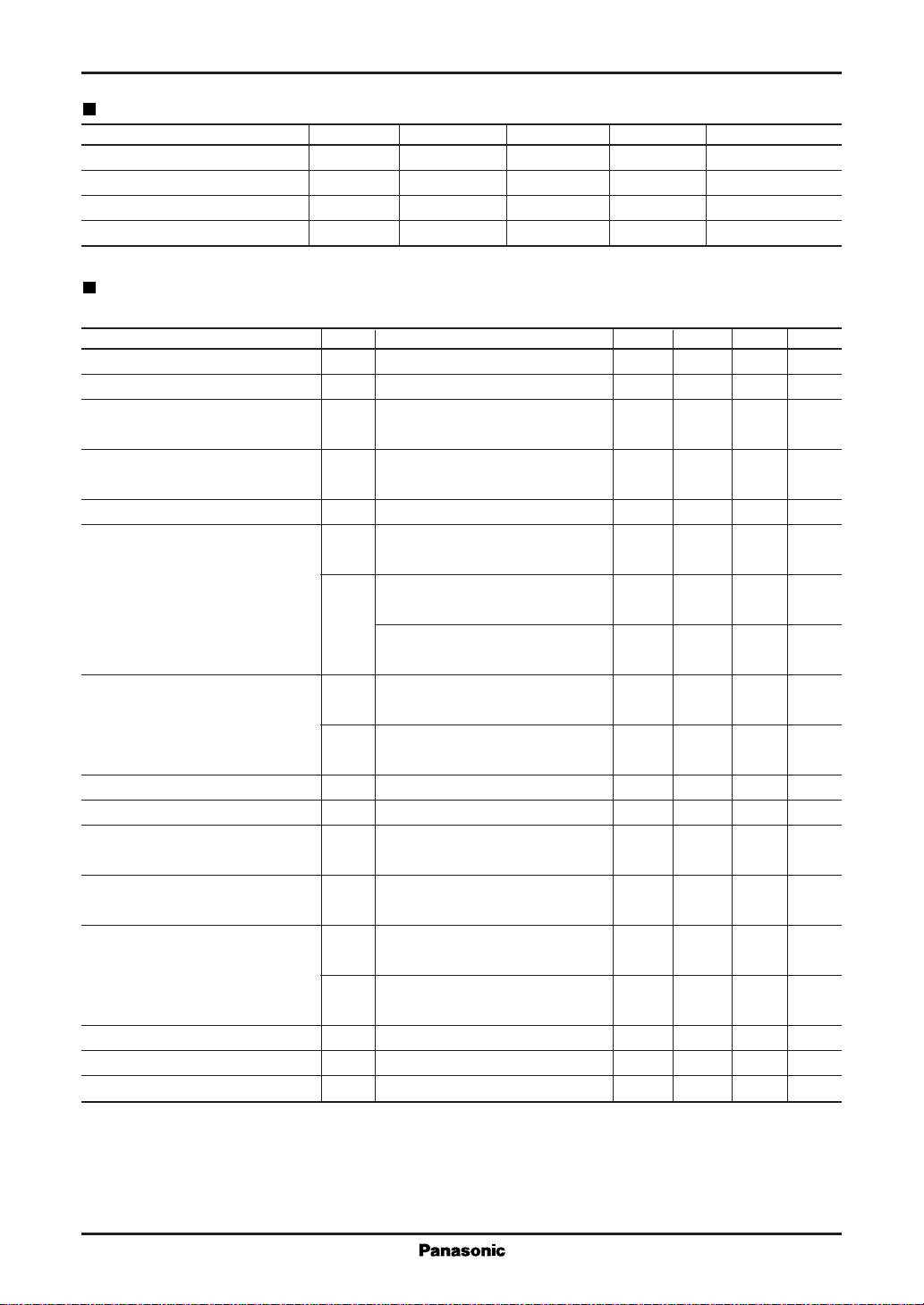
Operating Conditions
Parameter Symbol min typ max Unit
Power supply voltage V
Input clock frequency f
Input clock amplitude (sine wave) V
DD
ck
ck
Ambient temperature Ta –20 60 ˚C
Electrical Characteristics
VDD=5.0V, Vck=0.3V
Parameter Symbol Conditions min typ max Unit
Power supply voltage I
Insertion gain for VOC pin IG f
Total harmonic distortion for VOC THD f
pin
Signal-to-noise ratio for VOC pin S/N 3.264 86 MHz output (V
Output impedance for VOC pin Z
Comb characteristics for VOC pin
Clock leak for VOC pin
Signal bandwidth for VOY pin BW –3 dB for 196.7 kHz 2.5 5.5 MHz
Insertion gain for VOY pin IG f
Total harmonic distortion for VOY THD f
pin
Signal-to-noise ratio for VOY pin S/N Signal output (P–P)/noise output 48 56 dB
Clock leak for VOY pin
Delay for VOY pin τ
Output impedance for VOY pin Z
Crosstalk CT f
(sine wave), Vin=0.5V
P-P
P-P
DD
O
Com1
Com2
NC1
NC2
NC3
NC4
D
O
4.75 5.00 5.25 V
3.579545 MHz
0.25 0.3 1.0 V
(sine wave), fck=3.579545MHz, f=196.7kHz, Ta=25˚C
Average current 55 80 mA
=3.579545MHz –9 –5.5 –2 dB
sig
=3.26486MHz 0.5 2.5 %
sig
)/ 48 56 dB
P-P
noise output (rms)
300 600 Ω
3.571678MHz/3.579545MHz
(fsc–1/2fH) / (fsc)
3.256993MHz/3.264860MHz
(fsc–20.5fH) / (fsc–20fH)
3.902097MHz/3.894230MHz
(fsc–20.5fH) / (fsc–20fH)
3.58-MHz component/main
signal in output signal
14.32-MHz component/main
signal in output signal
=196.7kHz –1.5 1.5 4.5 dB
sig
=196.7MHz 1 4.5 %
sig
–35 –25 dB
–30 –20 dB
–30 –20 dB
–50 –40 dB
–30 –20 dB
(rms)
3.58-MHz component/main
signal in output signal
14.32-MHz component/main
signal in output signal
–50 –40 dB
–20 –10 dB
63.46 µs
250 500 Ω
=196.7kHz –32 dB
sig
P–P
4
Page 5
CCD Delay Line Series MN3870S
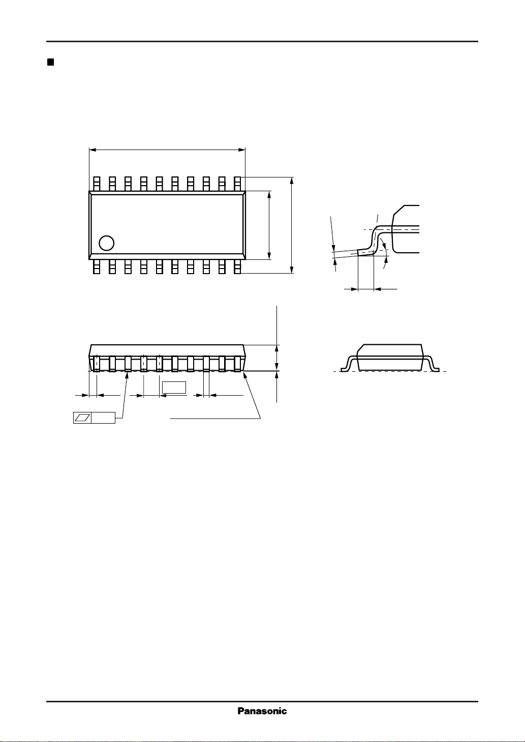
Package Dimensions (Unit:mm)
SOP020-P-0300C
12.63
±0.3
20
1
(0.6)
0.10
11
10
1.27
0.4±0.25
SEATING PLANE
5.5±0.3
2.05±0.2
0.1±0.1
7.6±0.3
0.05
-
+0.10
0.2
0 to 10°
(0.4)
5
Page 6

 Loading...