

Page 1
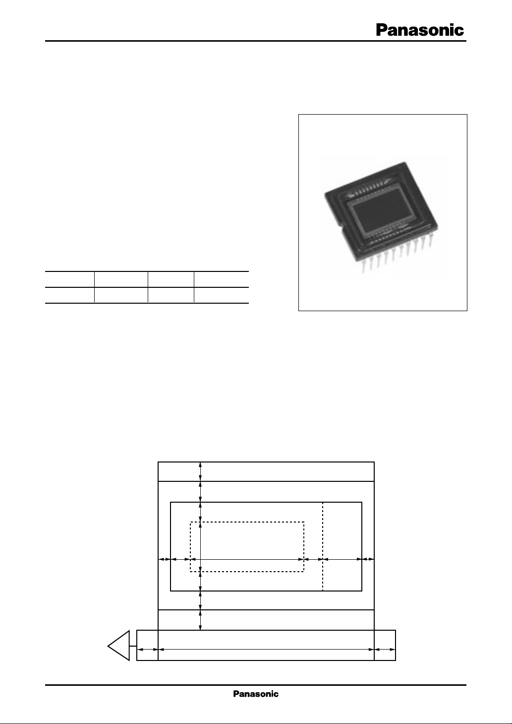
CCD Area Image Sensor
MN39571PT
9.2mm (type-1/2) 2,310k pixel CCD Area Image Sensor
■ Overview
The MN39571PT is a super high resolution CCD area
image sensor which includes 2,310k pixels in type-1/2
image format size.
Adopting RGB Bayer arrangement in primary color filter
array on chip provides excellent color reproduction. As
the aspect ratio of image area is 3:2 which is the same as
that of 35mm film, pictures can be taken in similar framing manner to use of a usual film camera.
As The MN39571PT has also a skipping readout mode
for image monitoring by LCD panel,you can fix the composition in real time.
Part Number
MN39571PT
Size System Color or B/W
9.2mm(type-1/2)
IS Color
■ Features
• Photographic grade super high resolution by 2,310k
pixels in type-1/2 format
• Responds to 5:1 skipping readout mode for LCD moni-
toring
• The same aspect ratio of 3:2 as a 35mm film
• Newly developed small plastic package
Outline dimensions : 14.0mm(W) × 12.4mm(D) ×
3.4mm(t)(Without lead pins)
■ Applications
• Digital still camera
• FA, OA cameras
■ Device Configuration Diagram
For transient (PD exists)
1200 224
8
1800
Vertical dummy bit (No PD)
Al shielding (PD exists)
Valid pixels
OB part
88122
424
13 1901
Vertical dummy bit (No PD)
Effective horizontal CCD
Horizontal dummy bitHorizontal dummy bit
1
1
Page 2
MN39571PT CCD Area Image Sensor
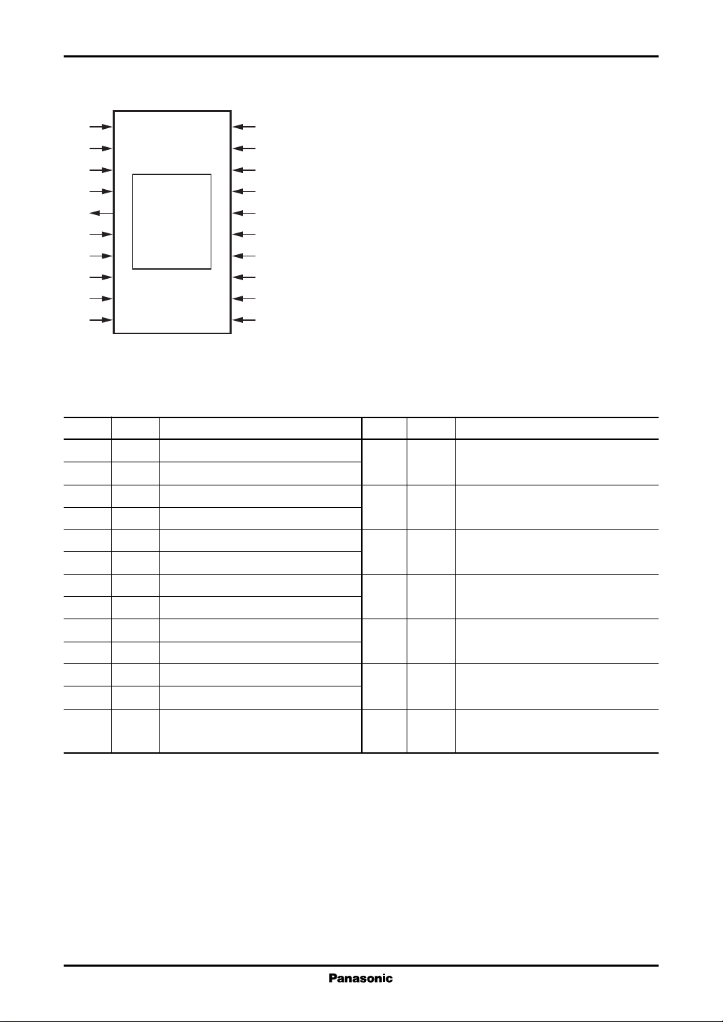
■ Pin Assignments
PW
RG
RD
OD
VO
LG
OG
φ
H1
H2
1
2
3
4
5
6
7
8
20
19
18
17
16
15
14
13
912φ
φ
φ
φ
φ
φ
φ
φ
φ
PT
V1
V2
V3
V4
V5
V6
V7
V8
10 11Sub IS
(T op V iew)
■ Pin Descriptions
Pin No. Symbol Descriptions
1 PW P-well
2 RG Reset gate
3 RD Reset drain
4 OD Output drain
5 VO Video output
6 LG Output load transistor gate
7 OG Output gate
8 φ
9 φ
10 Sub Substrate
11 IS Horizontal CCD input source
12 PT P-well for protection circuit
Horizontal register clock pulse (1)
H1
Horizontal register clock pulse (2)
H2
Pin No. Symbol Descriptions
14 φ
Vertical shift register
V7
clock pulse 7
15 φ
Vertical shift register
V6
clock pulse 6
16 φ
Vertical shift register
V5
clock pulse 5
17 φ
Vertical shift register
V4
clock pulse 4
18 φ
Vertical shift register
V3
clock pulse 3
19 φ
Vertical shift register
V2
clock pulse 2
13 φ
2
Vertical shift register
V8
clock pulse 8
20 φ
Vertical shift register
V1
clock pulse 1
Page 3
CCD Area Image Sensor MN39571PT
φV
Sub
(V)
φV
Sub
"H"
φV
Sub
"L"
E
V
Sub
(V)
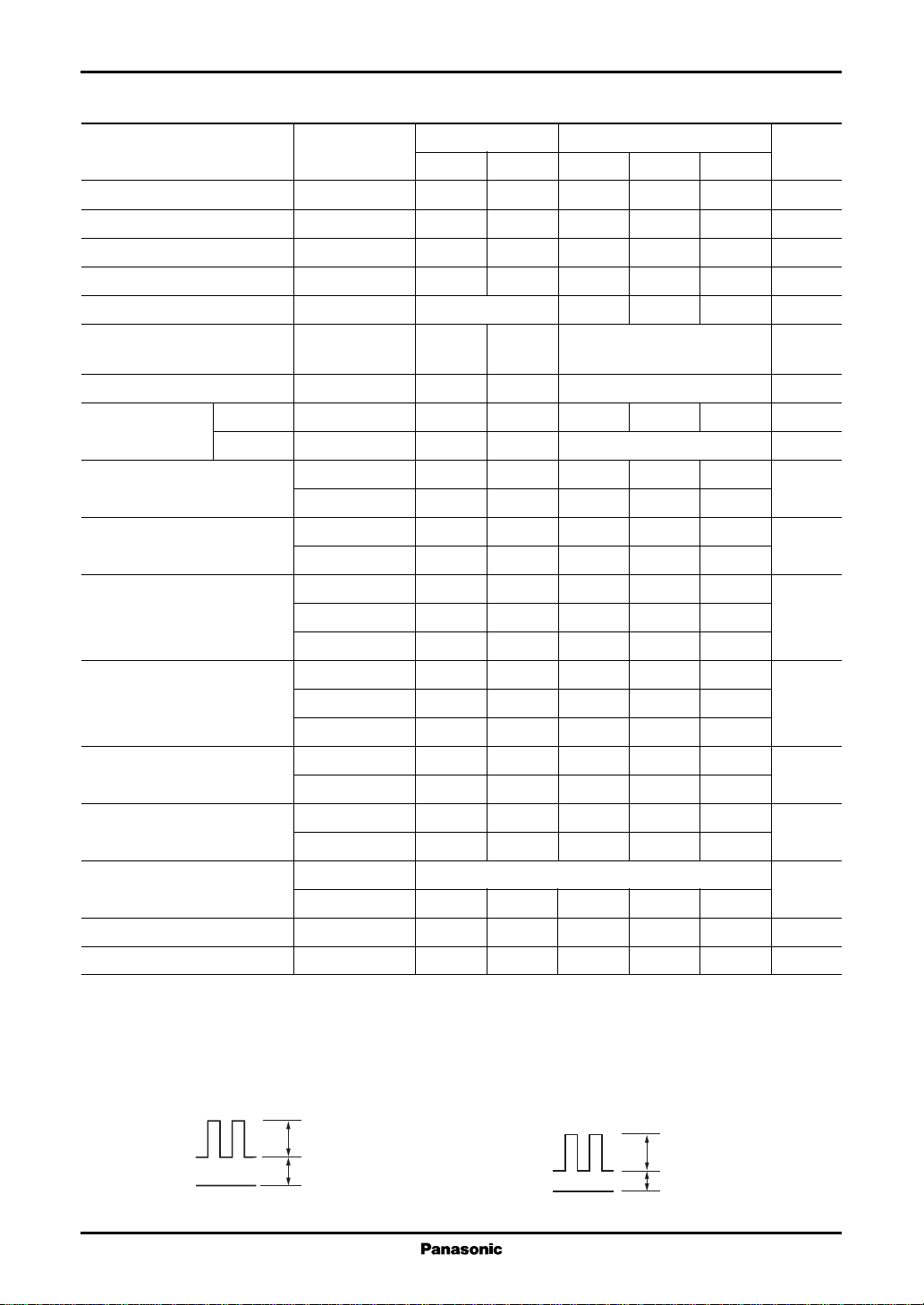
■ Absolute Maximum Ratings and Operating Conditions
Parameter Symbol
Output drain voltage V
Reset drain voltage V
Input source voltage V
Protection P-well voltage VPT
P-well voltage V
Output load transistor V
OD
RD
IS
*2
PW
LG
gate voltage
Output gate voltage V
Reset H-L V
pulse voltage Bias V
Horizontal register V
clock pulse voltage 1 V
Horizontal register V
clock pulse voltage 2 V
Vertical shift register V
clock pulse voltage 1,5 V
Vertical shift register V
clock pulse voltage 3,7 V
Vertical shift register V
clock pulse voltage 2,6 V
Vertical shift register V
clock pulse voltage 4,8 V
Substrate voltage V
Operating temperature T
Storage temperature T
Note
)1. Standard light input defines
Standard light input is the one when the exposure is done at a lens aperture of F8, using a light source of 2856 K and 1050 nt, and
placing a color temperature conversion filter LB-40 (HOYA) and an IR cutting filter CAW-500 (t = 2.5 mm) in the light path.
2. *1: V
3. *2: VPT is set so that the following conditions are set for VL of the vertical shift clock.
4. *3: 5. *4: V
6. *5: Separate powor supply is recommended for φV
internal settings guarantee blooming at 400 times light input of the standard light input.
Sub
<
VPT
VL
=
V
φR(H)
V
φR(L)
E
OG
φRG(H-L)
φRG(Bias)
φH1(H)
φH1(L)
φH2(H)
φH2(L)
φV1,5(H)
φV1,5(M)
V
φV1,5(L)
φV3,7(H)
φV3,7(M)
V
φV3,7(L)
φV2,6(M)
φV2,6(L)
φV4,8(M)
φV4,8(L)
*2
Sub
*4,*5
φV
Sub
opr
stg
H-L
Bias (Internally)
*3
*3
*2
*2
*2
*2
*2
*2
*2
*2
*2
*2
Rating Operating condition
min max min typ max
Unit
− 0.2 18.0 15.2 15.5 15.8 V
− 0.2 18.0 15.2 15.5 15.8 V
− 0.2 18.0 15.2 15.5 15.8 V
− 10.0 0.2 − 9.3 − 9.0 − 8.7 V
Reference voltage 0 V
Supplied internally V
Supplied internally V
8.0 3.0 3.3 3.6 V
− 0.5 Supplied internally V
8.0 3.0 3.3 3.6 V
− 0.2 − 0.2 0 0.2
8.0 3.0 3.3 3.6 V
− 0.2 − 0.2 0 0.2
18.0 15.2 15.5 15.8 V
− 0.2 0 0.2
− 10.0 − 9.3 − 9.0 − 8.7
18.0 15.2 15.5 15.8 V
− 0.2 0 0.2
− 10.0 − 9.3 − 9.0 − 8.7
15.0 − 0.2 0 0.2 V
− 10.0 − 9.3 − 9.0 − 8.7
15.0 − 0.2 0 0.2 V
− 10.0 − 9.3 − 9.0 − 8.7
Supplied internally V
− 0.2 45.0 26.5 27.0 27.5
− 10 60 25 °C
− 30 70 °C
when using electronic shutter function
Sub
Sub
3
Page 4
MN39571PT CCD Area Image Sensor
■ Optical Characteristics
Color
Effective
Part Number or pixels typ typ typ Sm typ typ typ
SaturationSensitivity
S/N
output F8
B/W H V (dB) (mV) (mV) typ(%)(%)
MN39571PT Color 1816 1208 500 340 0.01
Note
)1. 1/7.5 sec frame storage. Horizontal register clock frequency 24 MHz
2. *1: Mechanical shutter saturation output
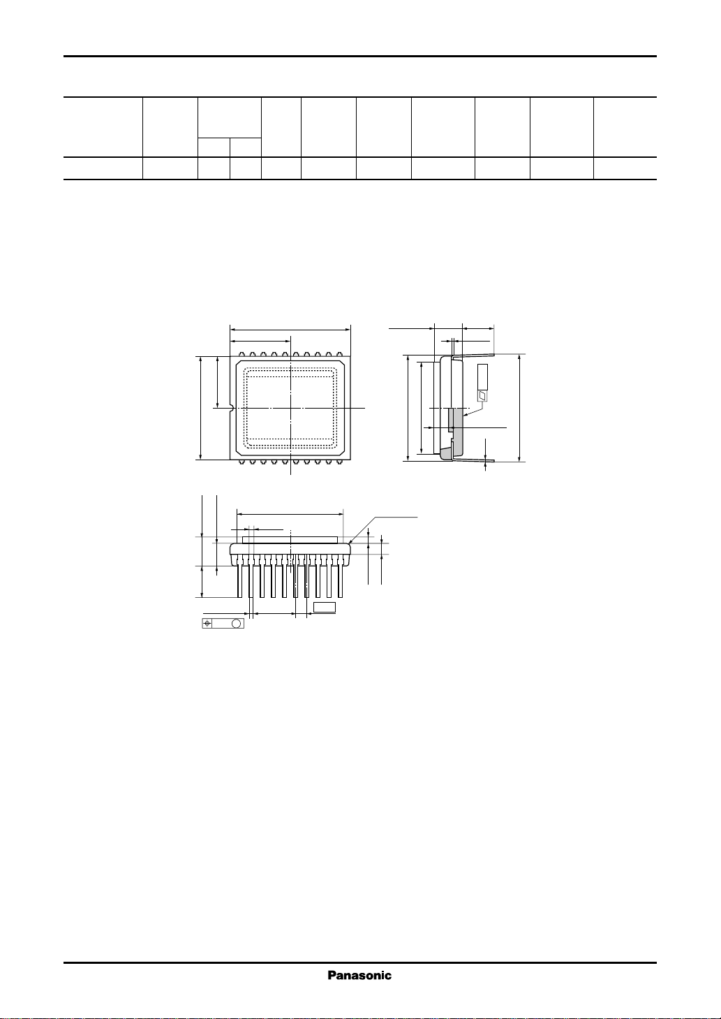
■ Package Dimensions (Unit : mm)
• WDIP020-P-0500A
Vertical
smear resolution resolution
Image lag
Horizontal Vertical
(TV-lines) (TV-lines)
12.40±0.08
3.40±0.15
3.90±0.15
0.30±0.05
14.00±0.08
7.00±0.08
20 11
6.20±0.08
110
12.60±0.10
2.60±0.15
0.46 M
(0.60)
(0.80)
1.27
3.40±0.30
R0.15 ns
(1.30)
(12.77)
11.60±0.10
3.90±0.15
(0.38)
0.015
1.71±0.10
0.25
12.95±0.25
4
 Loading...