

Page 1
For Video Equipment
MN3112SA
Vertical Driver for Video-Camera CCD Area-Image-Sensor
Overview
The MN3112SA is a vertical driver LSI incorporating
four vertical driver channels and one sub driver channel
for a 2-dimensional interline CCD image sensor.
The MN3112SA enables low current dissipation and
the part reductions.
Features
3V power supply for input section
Applications
Video cameras
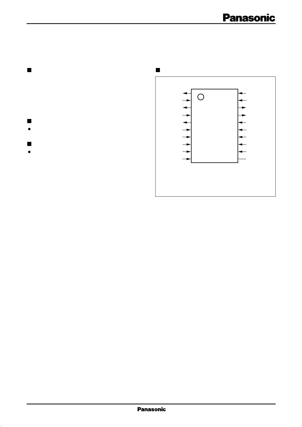
Pin Assignment
OSUB
V
OV2
V
M13
OV1
V
DC
IV1
CH1
IV2
ISUB
1
2
L
3
4
5
6
7
8
9
10
SSOP020-P-0225
(TOP VIEW)
20
19
18
17
16
15
14
13
12
11
V
HH
V
M24
OV4
OV3
V
H
GND
IV3
CH2
IV4
N.C.
Page 2
MN3112SA For Video Equipment
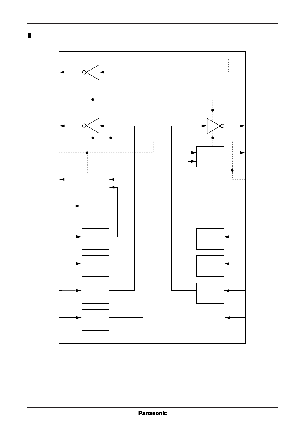
Block Diagram
OSUB
V
OV2
V
M13
OV1
V
DC
IV1
1
2
L
3
20
19
18
V
HH
V
M24
OV4
4
Tristate
17
OV3
driver
5
Tristate
16
V
H
driver
6
15
GND
7
Level
conversion
Level
conversion
14
IV3
CH1
IV2
ISUB
8
Level
conversion
9
Level
conversion
10
Level
conversion
V
, VL , GND : Common power supply
DC
V
, V
M13
V
, V
HH
: Binary and tristate independent power supplies for vertical driver section
M24
: Independent power supplies for sub driver section and vertical driver section
H
Level
conversion
Level
conversion
13
12
11
CH2
IV4
N.C.
Page 3
For Video Equipment MN3112SA
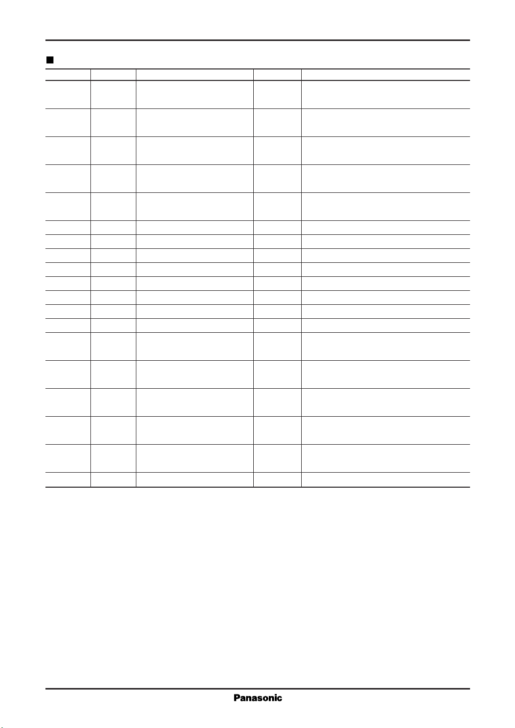
Pin Descriptions
Pin No. Symbol Pin Name I/O Function Description
6V
DC
15 GND Input section low-level
16 V
20 V
4V
19 V
2V
H
HH
M13
M24
L
9 IV2 Transfer pulse input I Charge transfer pulse input pin
12 IV4 Transfer pulse input I Charge transfer pulse input pin
7 IV1 Transfer pulse input I Charge transfer pulse input pin
14 IV3 Transfer pulse input I Charge transfer pulse input pin
8 CH1 Charge pulse input I Charge read pulse input pin
13 CH1 Charge pulse input I Charge read pulse input pin
10 ISUB SUB pulse input I Unwanted charge sourcing pulse input pin
18 OV4 Binary transfer pulse O Binary transfer pulse output pin
3 OV2 Binary transfer pulse O Binary transfer pulse output pin
17 OV3 Tristate transfer pulse O Tristate transfer pulse output pin
5 OV1 Tristate transfer pulse O Tristate transfer pulse output pin
1 OSUB SUB pulse output O Unwanted charge sourcing pulse output pin
11 N.C. No connection —
Input section high-level
power supply
power supply
Vertical driver section
high-level power supply
SUB driver section
high-level power supply
Middle-level power supply I
I 5V high-level input
I 5V low-level input
I High-level input at high-voltage section
I High-level input at high-voltage section
Middle-level input at high-voltage section
Input externally to both V
M13
and V
M24
Low-level power supply I Low-level input at high-voltage section
output (V
output (V
output (VH , V
output (VH , V
(V
M24
M24
HH
, VL)
, VL)
M13
M13
, VL)
, VL)
, VL)
.
Page 4
MN3112SA For Video Equipment
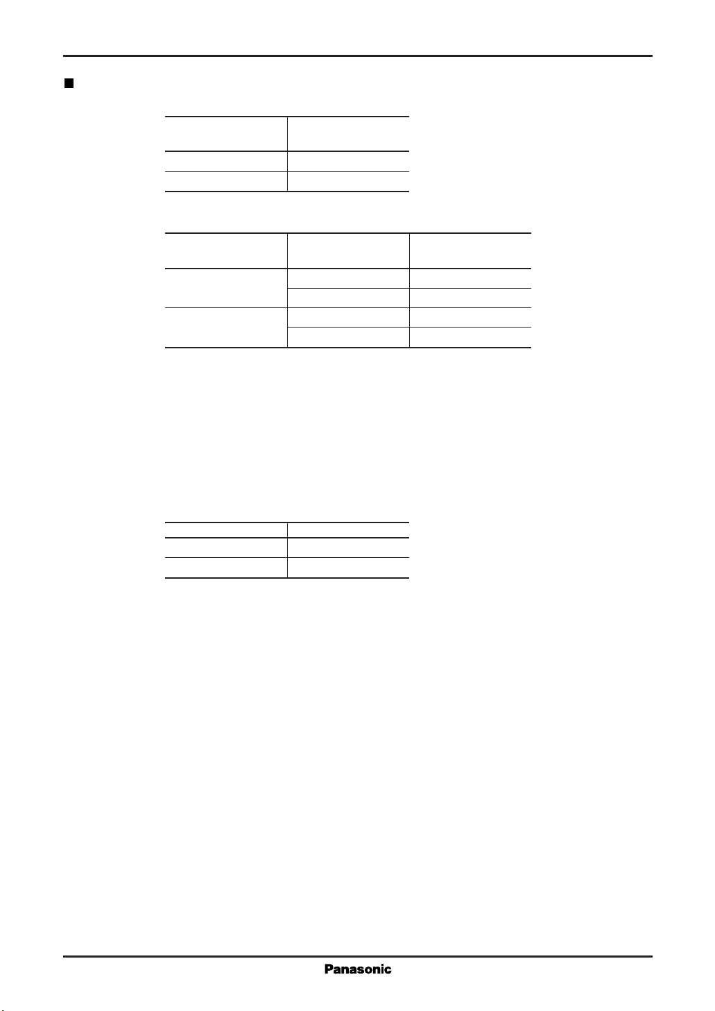
Functions
Binary transfer pulse (vertical driver section)
IV2 OV2
IV4 OV4
HL
LM
Tristate transfer pulse (vertical driver section)
CH1 IV1 OV1
CH2 IV3 OV3
H
L
1
*
IV1, IV2, IV3, IV4, CH1, CH2
H: V
DC
L: GND
OV1, OV2, OV3, OV4
H: V
H
M: V
or V
M13
M24
L: V
L
HL
LM
HL
LH
Unwanted charge sourcing pulse (SUB driver section)
ISUB OSUB
HL
LH
1
*
ISUB
H: V
DC
L: GND
OSUB
H: V
HH
L: V
L
Page 5
For Video Equipment MN3112SA
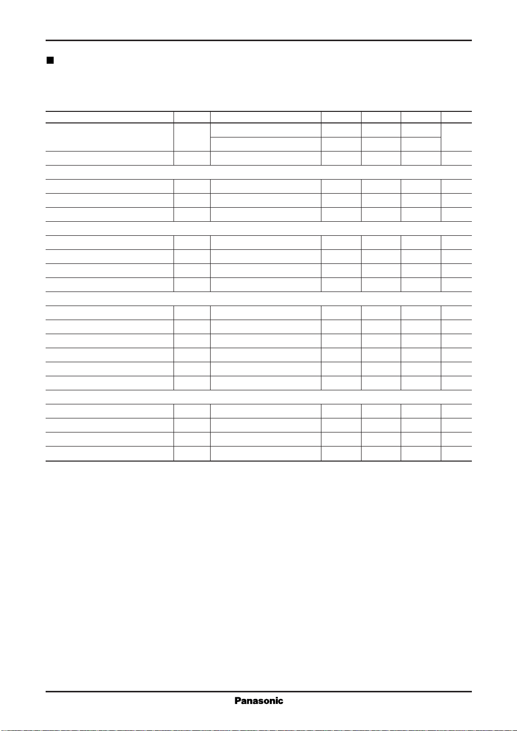
Electrical Characteristics
(1) DC characteristics
VHH=18.0V , VH=13.0V , V
VDC=5.00V , GND=0.0V , Ta= –10˚C to +70˚C
M13=VM24
Parameter Symbol Test Conditions min typ max Unit
Quiescent supply current I
Operating supply current I
Input pins IV1 , IV2 , IV3 , IV4 , CH1 , CH2 , ISUB
Voltage "H" level V
Voltage "L" level V
Input leakage current I
Output pins 1 (binary output) OV2 , OV4
Output voltage middle level V
Output voltage "L" level V
Output on-resistance middle level R
Output on-resistance "L" level R
Output pins 2 (tristate output) OV1 , OV3
Output voltage "H" level V
Output voltage middle level V
Output voltage "L" level V
Output on-resistance "H" level R
Output on-resistance middle level R
Output on-resistance "L" level R
Output pin 3 (SUB output) OSUB
Output voltage "H" level V
Output voltage "L" level V
Output on-resistance middle level R
Output on-resistance "L" level R
=1.0V , VL= –7.0V,
DDST
VI=GND , VDC=3.0V 2.5
VI=GND , VDC=5.0V 4
DDDYNVI
IH
IL
LI
OM1IOM1
OL1IOL1
ONM1IOM1
ONL1IOL1
OH2IOH2
OM2IOM2
OL2IOL2
ONH2IOH2
ONM2IOM2
ONL2IOL2
OHH3IOHH3
OL3IOL3
ONHH3IONHH3
ONL3IONL3
=GND , V
VI=0 to 5V ±1 µA
= –1mA 0.9 V
=1mA V
=–50mA 40 Ω
=50mA 40 Ω
=–1mA 12.9 V
=–1mA 0.9 V
=1mA V
=–50mA 50 Ω
=±50mA 40 Ω
=50mA 40 Ω
=–1mA 17.9 V
=1mA V
=50mA 40 Ω
mA
DC
0.7 × V
DC
GND 0.3 × V
L
L
L
7mA
V
DC
DC
M24
—V
H
M13
—V
HH
—V
=–50mA 50 Ω
V
V
V
V
V
V
Page 6
MN3112SA For Video Equipment
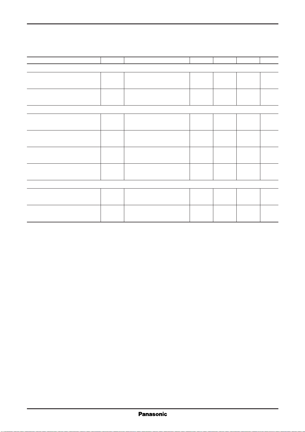
(2) AC characteristics
=18.0V , VH=13.0V , V
V
HH
=3.0V , GND=0.0V , Ta=–10˚C to +70˚C
V
DC
M13=VM24
Parameter Symbol Test Conditions min typ max Unit
Output pins 1 (binary output) OV2 , OV4
Transmission delay time t
Rise time t
Fall time t
Output pins 2 (tristate output) OV1 , OV3
Transmission delay time t
Transmission delay time t
Rise time t
Fall time t
Rise time t
Fall time t
Output pin 3 (SUB output) OSUB
Transmission delay time t
Rise time t
Fall time t
=1.0V , VL=–7.0V,
PLM
t
PML
TLM
TML
PLM
t
PML
TMH
t
THM
TLM
TML
TMH
THM
PLHH
t
PHHL
TLHH
THHL
No load
"L" level — middle level
No load
"L" level — middle level
No load
middle level — "H" level
No load
"L" level — "H" level
100 200 ns
200 300 ns
100 200 ns
200 400 ns
200 300 ns
200 300 ns
100 200 ns
200 300 ns
Page 7
For Video Equipment MN3112SA
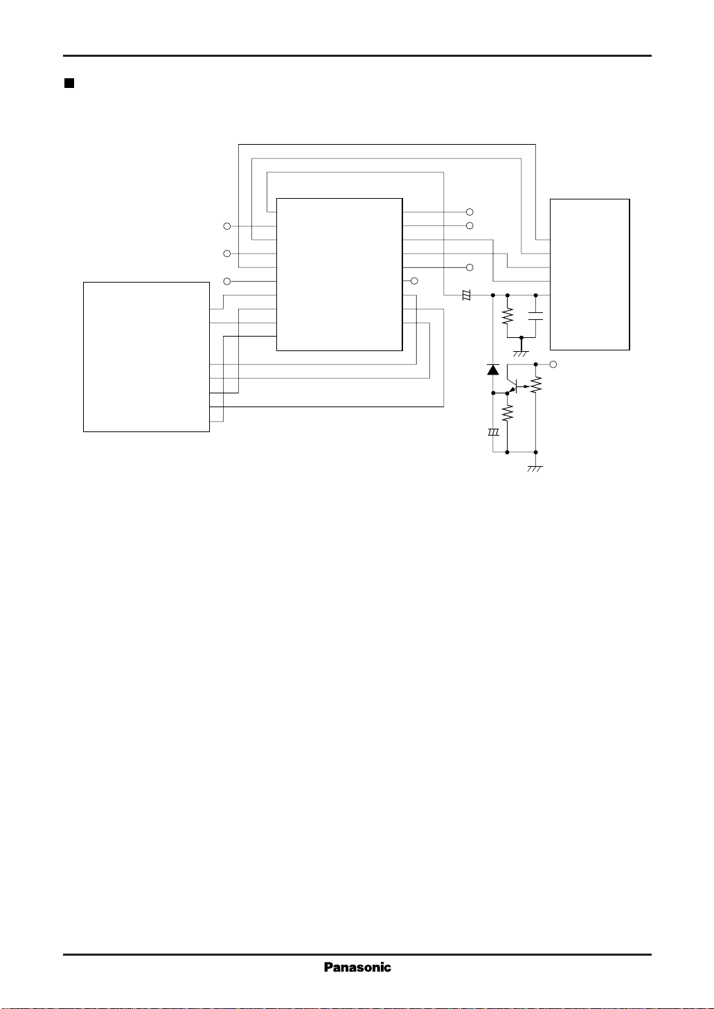
Application Circuit Example
510H
CCD image sensor
MN3112SA
1 OSUB
2 V
L
3 OV2
4 V
M13
5 OV1
6 V
DC
CCD drive logic
MN5151
V
L
V
M13
V
DC
7 IV1
V1 19
V2 18
8 CH1
9 IV2
10 ISUB
V3 15
V4 14
CH1 13
CH2 12
SUB 11
Note *1: Connect a bypass capacitor as close as possible to each of the MN3112SA’s power supply pins (V
V
, VL , VDC).
M24
V
20
HH
19
V
M24
OV4 18
OV3 17
16
V
H
GND 15
IV3 14
CH2 13
IV4 12
N.C. 11
GND
3.3µF/50V
V
V
V
3.3µF/50V
+
H
HH
M24
+
1MΩ
2200pF
47kΩ
MN3716
12 øV1
13 øV2
14 øV3
15 øV4
10 SUB
+16V
200kΩ
, VH , V
HH
M13
,
Page 8
MN3112SA For Video Equipment
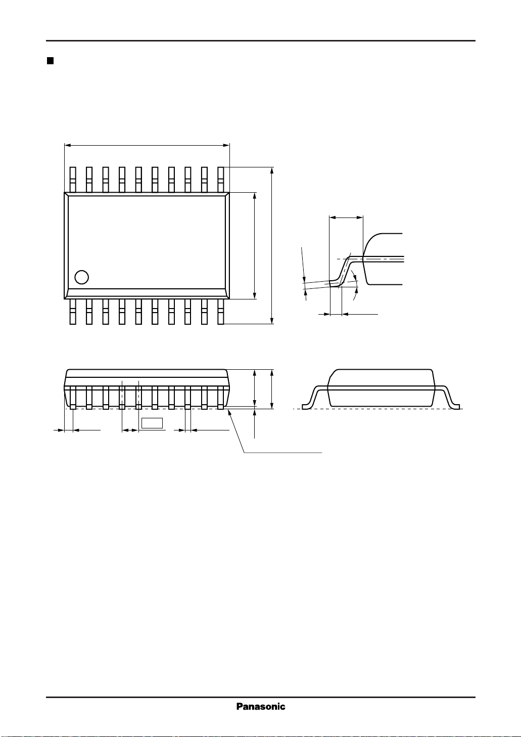
Package Dimensions (Unit: mm)
SSOP020-P-0225
6.5±0.2
20
11
1.0±0.2
6.3±0.3
0.05
-
+0.10
4.3±0.21.5±0.2
0.15
0.3min.
110
1.9max.
(0.33)
0.65
0.25±0.10
0.1±0.1
SEATING PLANE
0 to 10°
Page 9
For Video Equipment MN3112SA
Usage Notes
(1) When the sub driver is not used
1. Connect V
2. Connect ISUB (pin 10) to V
3. Make no connection for OSUB (pin 1).
(2) Connect a bypass capacitor as close as possible to MN3112SA power supply pins V
V
(pin 4), V
M13
(3) Guarantee period after unsealing
The guarantee period after opening the dry-sealed packaging is three weeks under the environment
conditions of 30˚C/70% (temperature/humidity).
(4) The recommended reflow temperature is 230˚C.
(pin 20) to VH (pin 16).
HH
(pin 6) or GND (pin 15).
DC
(pin 19), VL (pin 2), and VDC (pin 6).
M24
(pin 20), VH (pin 16),
HH
 Loading...