

Page 1
CCD Delay Line Series
MN3883S
Full Multi-PAL-Compatible CCD Video Signal Delay Element
Overview
The MN3883S is a CCD signal delay element for video
signal processing applications.
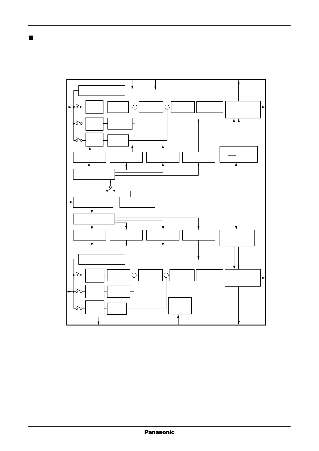
It contains such components as a shift register clock
driver, charge I/O blocks, 1/2nd frequency doubler, two
switchable CCD analog shift registers, a clamp bias circuit, resampling output amplifiers, a mode selection circuit and booster circuits.
When the switch input is "H" level, the MN3883S
samples the input using the supplied clock signal with a
frequency 7.15909 MHz of twice the NTSC color signal
subcarrier frequency, and after adding in the attached filter delay, produces independent delays of 1 H (the horizontal scan period for the NTSC system) each for the
two lines.
When the switch input is "M" level, the MN3883S
samples the input using the supplied clock signal with a
frequency 8.8672375 MHz of twice the PAL color signal
subcarrier frequency, and after adding in the attached filter delay, produces independent delays of 1 H (the horizontal scan period for the NTSC system) each for the
two lines.
When the switch input is "L" level, the MN3883S
samples the input using the supplied clock signal with a
frequency 8.8672375 MHz of twice the PAL color signal
subcarrier frequency, and after adding in the attached filter delay, produces independent delays of 1 H (the horizontal scan period for the PAL system) for the Y output
and 2 H for the C output.
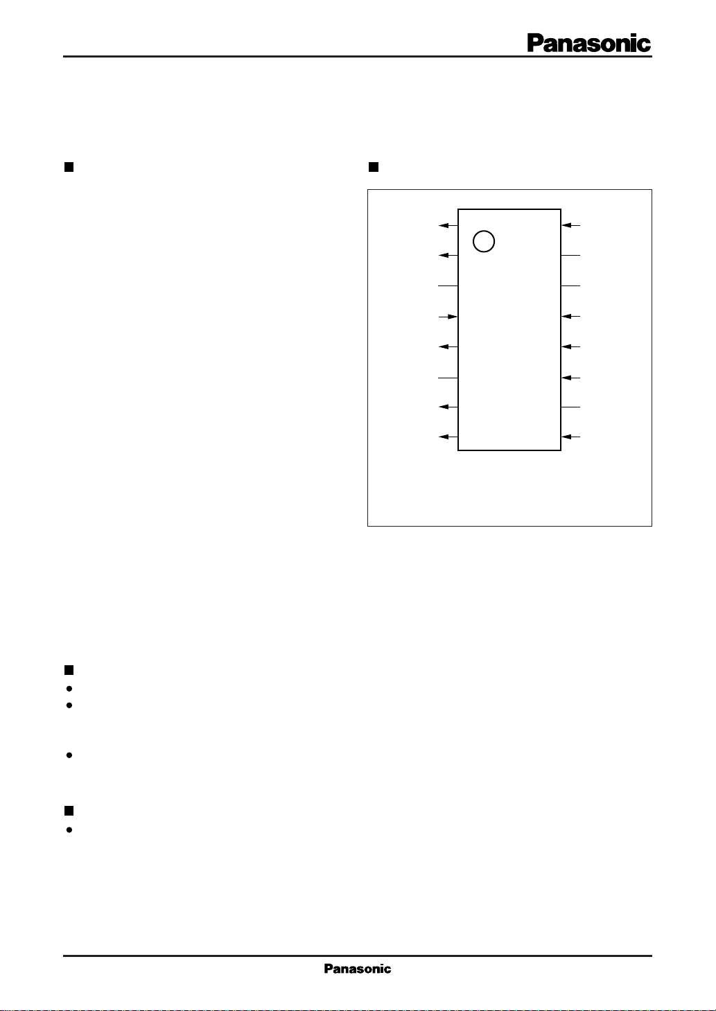
Pin Assignment
VBIASC
VOC
N.C.
V
DD
–V
BB
N.C.
VOY
VBIASY
1
2
3
4
5
6
7
8
SOP016-P-0225
( TOP VIEW )
VINC
16
N.C.
15
N.C.
14
XI
13
V
12
11
10
9
SS
SW
N.C.
VINY
Features
Single 4.9 V power supply
Single chip combining luminance signal delay element
and delay element for color signal converted to low
frequency
Full Multi-PAL support, switchable between NTSC,
4.43 NTSC, and PAL systems
Applications
Full multi-PAL-compatible VCRs
1
Page 2
MN3883S CCD Delay Line Series
Block Diagram
VINC
XI
Bias circuit
P
443N
N
Charge
input
block
Charge
input
block
Charge
input
block
16
øS driver ø1 driver
Timing adjustment
N
443N
13
Waveform amplifier
adjustment block
Timing adjustment
øS driver ø1 driver
CCD
8 stages
CCD
3.5 stages
CCD
3 stages
P
1/2nd frequency
doubler
SS
V
12
+
DD
V
4
CCD
108 stages
CCD
+
451 stages
ø2 driver øR driver
ø2 driver øR driver
Charge
detection
block
VBIASC
1
Resampling
output amplifier
øSH driver
øSH driver
øSH driver
øSH driver
2
VOC
Clamp circuit
P
VINY
9
443N
N
Charge
input
block
Charge
input
block
Charge
input
block
5
BB
-V
CCD
7.5 stages
CCD
3.5 stages
CCD
3 stages
CCD
++
108 stages
CCD
451 stages
Mode
selection
circuit
11
SW
Charge detection block
Resampling
output amplifier
8
7
VOY
VBIASY
Three input levels: H: NTSC
M: 4.43 NTSC
L: PAL
2
Page 3
CCD Delay Line Series MN3883S
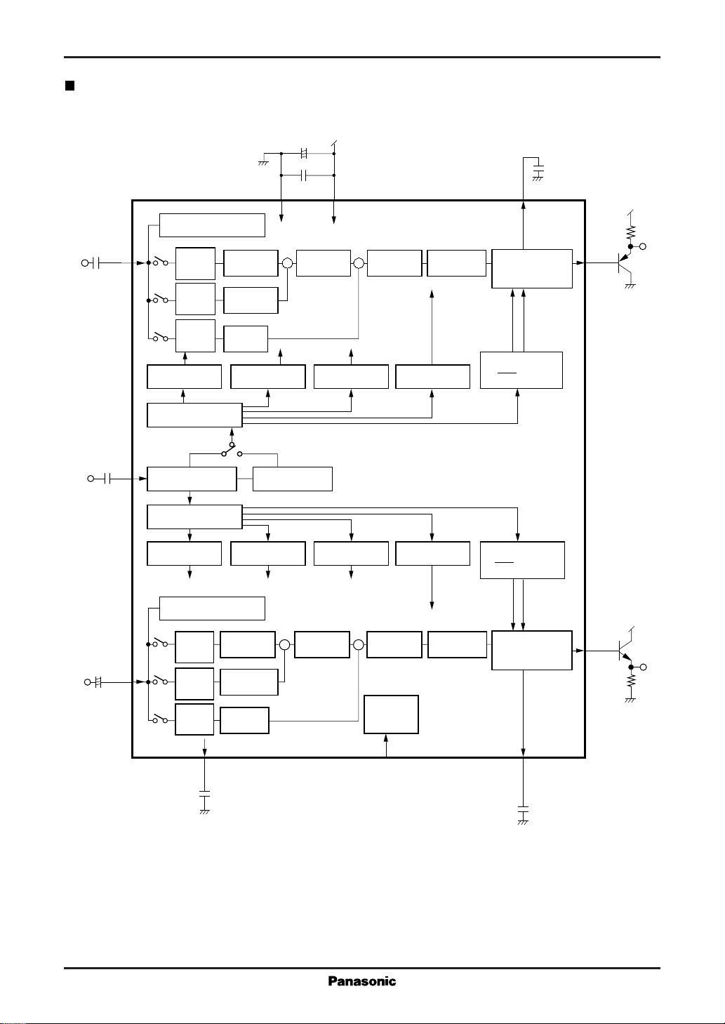
Application Circuit Example
10µF
–
+
(0.01µF)
VINC
(0.01µF)
Bias circuit
P
16
443N
N
Charge
input
block
Charge
input
block
Charge
input
block
øS driver ø1 driver
Timing adjustment
N
443N
CCD
8 stages
CCD
3.5 stages
CCD
3 stages
P
SS
V
12
+
DD
0.1µF
V
4
CCD
108 stages
+
ø2 driver øR driver
CCD
451 stages
Charge detection block
VBIASC
1
Resampling
output amplifier
øSH driver
øSH driver
2
VOC
1000pF
–
0.47µF
XI
VINY
+
13
Waveform amplifier
adjustment block
Timing adjustment
øS driver ø1 driver
Clamp circuit
P
Charge
input
block
443N
9
Charge
input
block
N
Charge
input
block
5
BB
-V
(0.01µF)
1/2nd frequency
doubler
CCD
7.5 stages
CCD
3.5 stages
CCD
3 stages
ø2 driver øR driver
CCD
++
108 stages
CCD
451 stages
Mode
selection
circuit
11
SW
Three input levels:
H: NTSC
M: 4.43 NTSC
L: PAL
Charge detection block
øSH driver
øSH driver
Resampling
output amplifier
8
VBIASY
(0.01µF)
7
VOY
Note: When an electlytic capacitor is attached to pin 5, connect the negative pole to pin 5.
3
Page 4
MN3883S CCD Delay Line Series
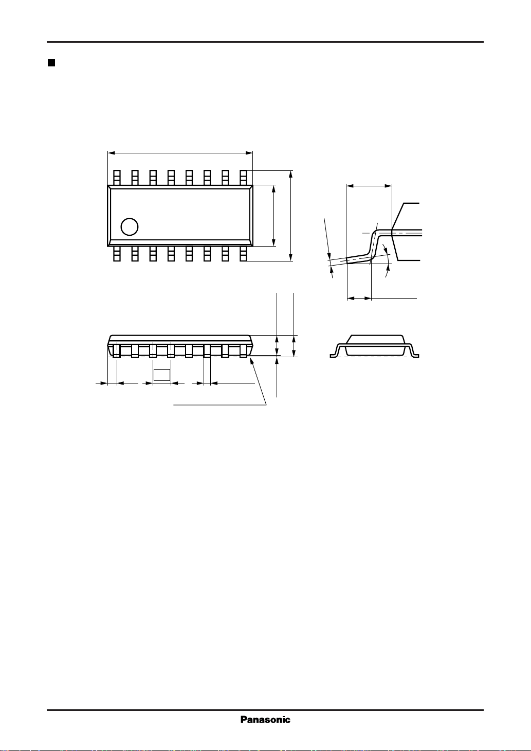
Package Dimensions (Unit:mm)
SOP016-P-0225
10.10
±0.20
16
9
1.10
±0.20
±0.20
0.05
-
6.50
+0.10
4.30
0.15
18
0.20
+0.50
-
±0.20
1.50
1.60
(0.6)
1.27
SEATING PLANE
0.40
±0.10
±0.10
0.10
±0.20
0 to 10°
0.40min.
4
 Loading...