

Page 1
CCD Delay Line Series
MN3890S
NTSC-Compatible CCD 1 H Video Signal Delay Element
Overview
The MN3890S is a 1 H image delay element of a 4 f
CMOS CCD and suitable for video signal processing applications.
It contains such components as a frequency-doubler
circuit, a shift register clock driver, a 906-stage CCD analog shift register, and a resampling output amplifier.
The MN3885S drives and samples the 906-stage analog shift register using a redoubled version of the supplied clock signal with a frequency 7.16 MHz of twice
the NTSC color signal subcarrier frequency , and after adding in the attached filter delay, produces a delay of 1 H
(the horizontal scan period).
Features
Single 5.0 V power supply
Energy-saving design based on CMOS process
Low EMI levels from clock during driving
Applications
VCRs, Video cameras
Structure and Operation
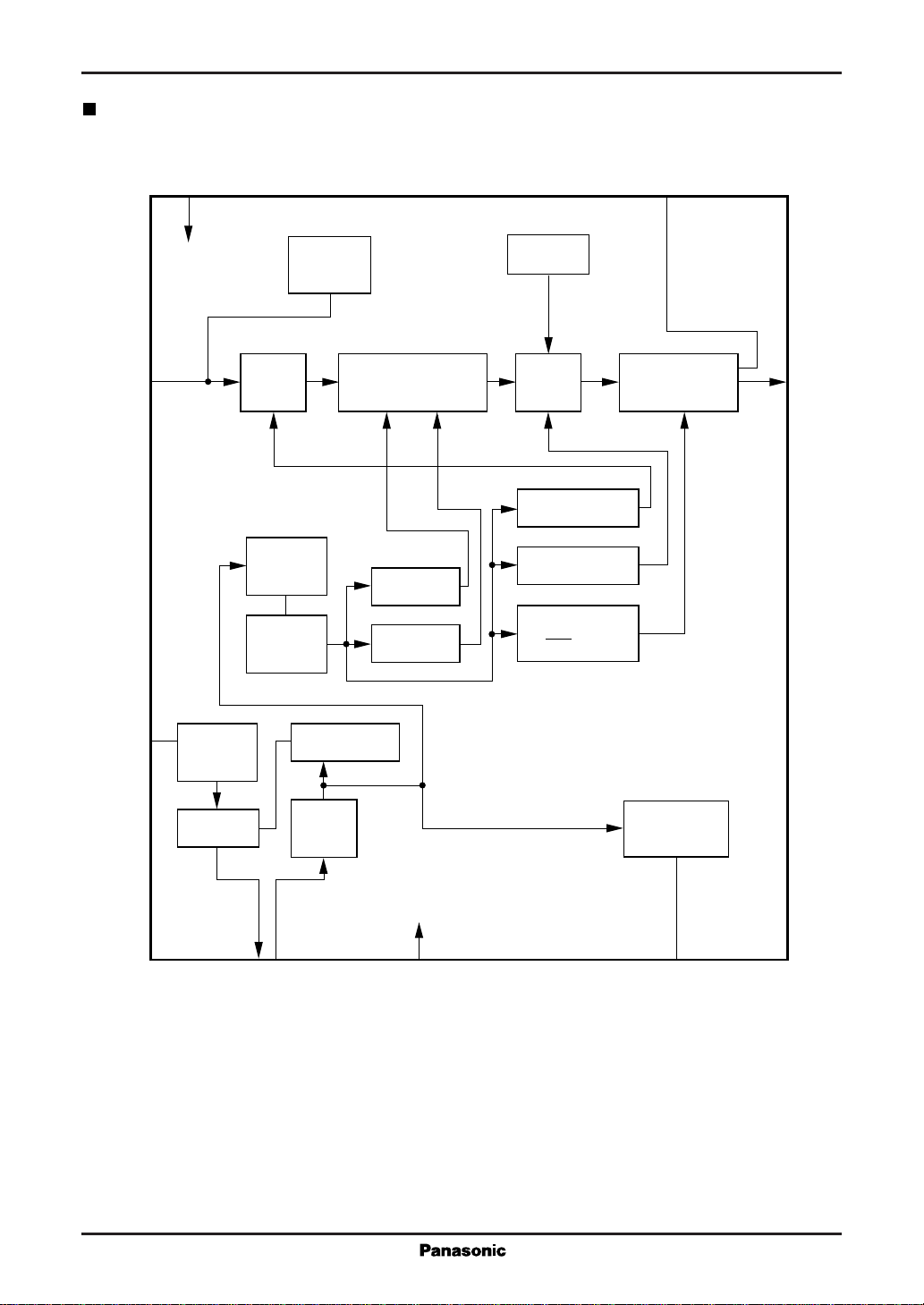
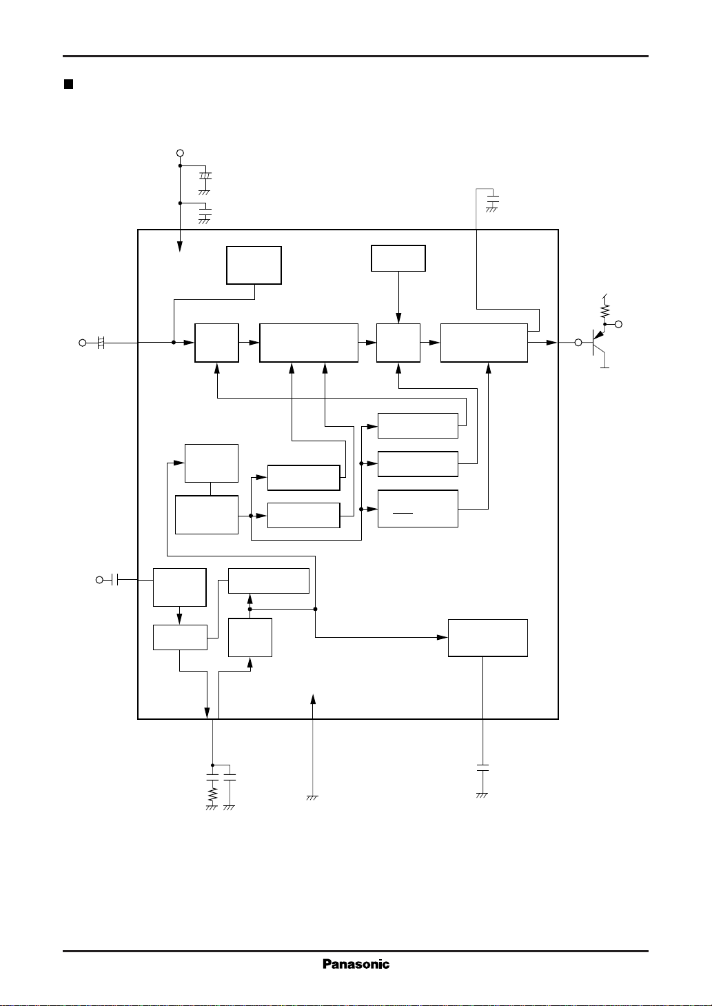
The MN3890S consists of the operational blocks shown
in the block diagram.
Frequency-doubler circuit
When the 7.16 MHz of the doubled NTSC color signal
subcarrier frequency is inputted from the clock input pin
XI, 14.32 MHz clock of fourfold frequency of color signal subcarrier is generated by this circuit.
Clock driver
This block generates two transfer clock signals, ø1 and
ø2, synchronized with the 14.32 MHz clock signal from
the frequency-doubler circuit.
It also generates the sampling clock signals øS and øS',
resampling clock signal øSH, and reset clock signal øR
that have adjusted timing relations with ø1 and ø2.
CCD analog shift register
This block first converts the analog signal fr om the V
input signal pin into a voltage signal, and inputs it into
906-stage analog shift register.
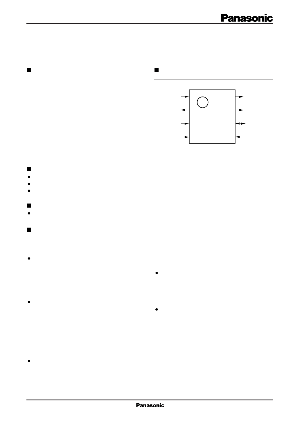
Pin Assignment
SC
BB
DD
1
IN
2
3
4
SS
8
7
6
5
( TOP VIEW )
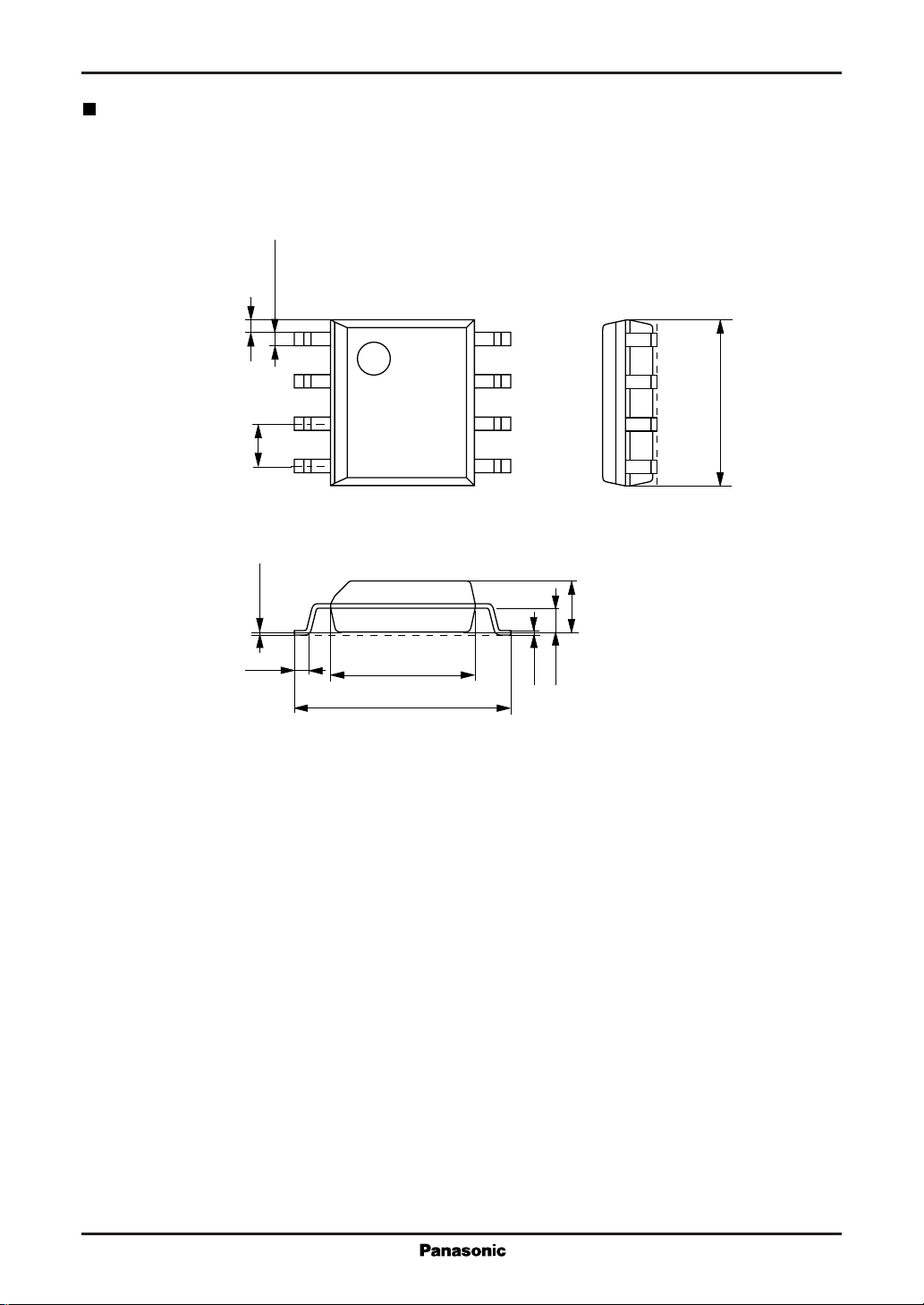
SOP008-P-0225A
output pin at the point
O
V
V
V
V
The shift register samples the shift register input with
the sampling clock øS, and converts the results to char ges,
and uses transfer clocks ø1 and ø2 to transfer the results
to the following block, the charge detection block, where
the charges is converted into a voltage signal.
Resampling output amplifier
In the output amplifier, this voltage signal is done
Sample-and-Hold by resampling, and Y-signal as it is
outputted at Vo.
Operation
The following is an explanation of delay line operation.
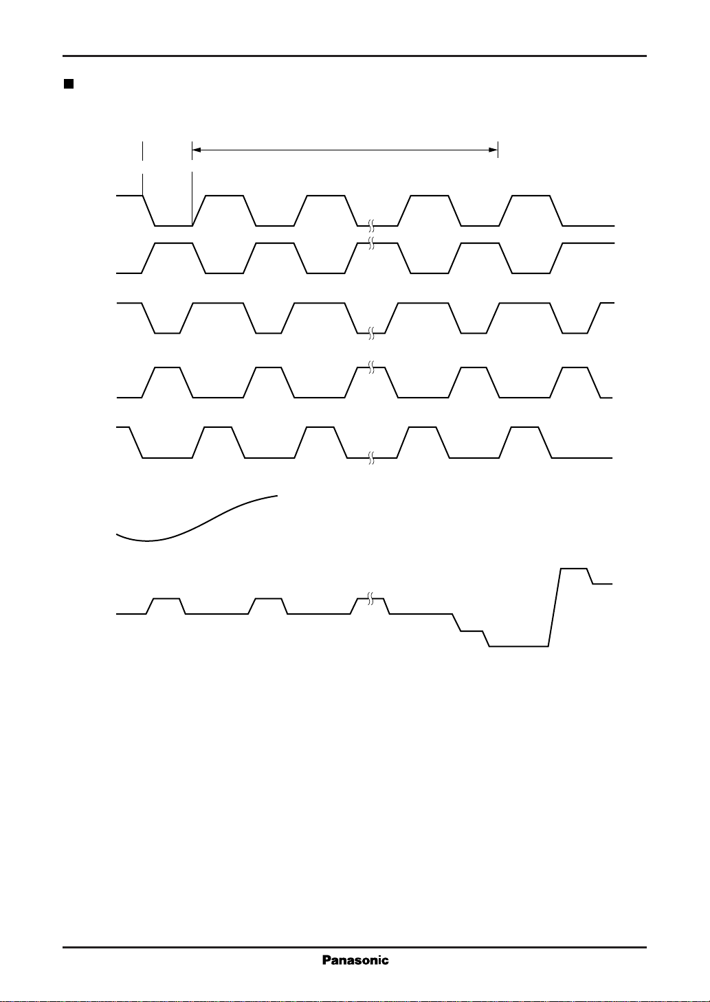
The waveforms driving the shift registers are as shown
in the timing chart on page 622.
The input signal voltage sampled during the interval
between t=0 and t=τc (where τc is one-half the sampling
interval) appears at the V
t=1813τc.
IN
V
O
V
GC
PCOUT
&
VCOIN
XI
1
Page 2
MN3890S CCD Delay Line Series
Block Diagram
DD
V
3
GC
V
7
Booster
Bias circuit
1
V
IN
Charge
input
CCD 906 stages
block
circuit
Charge
detection
block
Resampling
output amplifier
8
V
O
øS driver
Waveform
adjustment
block
ø1 driver
øR driver
øSH driver
Timing
adjustment
ø2 driver
øSH driver
XI
5
amplifier
adjustment
block
Phase
comparator
6
PCOUT
1/2nd frequency
doubler
VCO
&
VCOIN
Substrate bias
generator
4
SS
V
2
BB
V
Waveform
2
Page 3
CCD Delay Line Series MN3890S
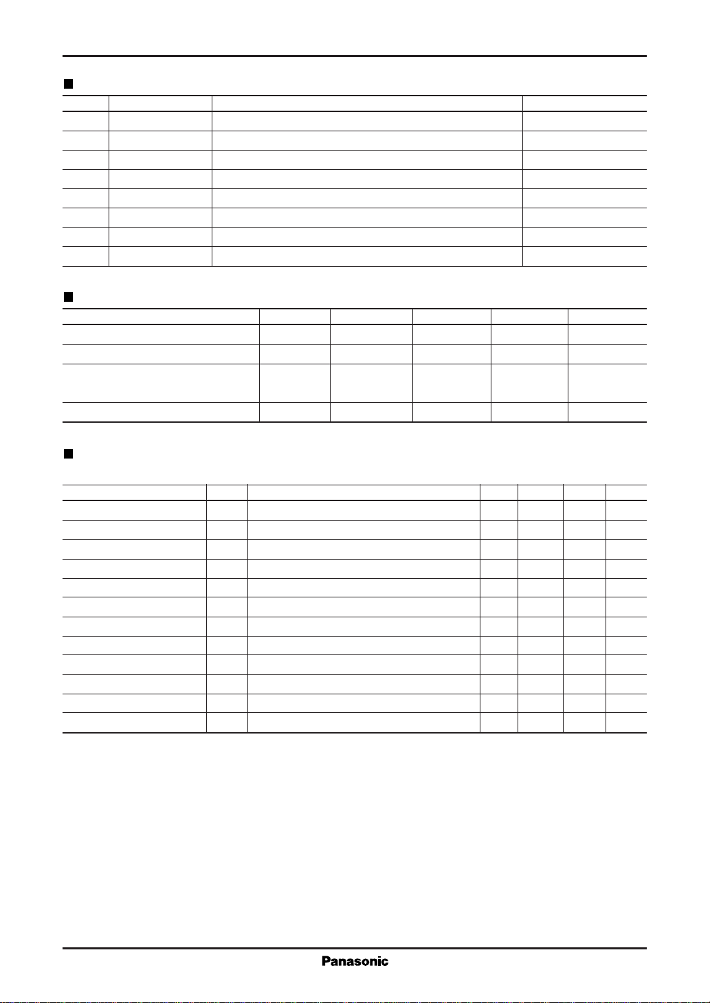
Pin Descriptions
Pin No. Symbol Function Description Remarks
1VINSignal input pin
2VBBSubstrate connection pin Negative voltage pin
3VDDPower supply
4VSSGround
5 XI 7.16 MHz clock input pin
6 PCOUT & VCOIN Phase comparator output and voltage controlled oscillator input
7VGCOutput gate connection pin
8VOSignal output pin
Operating Conditions
Parameter Symbol min typ max Unit
Power supply voltage V
Input clock frequency f
Signal bandwidth Input clock amplitude
(sine wave)
DD
ck
V
ck
Ambient temperature Ta –20 60 ˚C
4.75 5.00 5.25 V
7.15909 MHz
0.2 0.3 1.0 V
P–P
Electrical Characteristics
VDD=5.0V, Vck=0.3V
Parameter Symbol Conditions min typ max Unit
Power supply current I
Signal bandwidth BW –3 dB for 200 kHz value 2.5 5.5 MHz
Insertion gain IG f
Total harmonic distortion THD f
Signal-to-noise ratio S/N Signal output (V
Clock leak 1 NC1 7.16 MHz component/main output signal –50 –40 dB
Clock leak 2 NC2 14.32 MHz component/main output signal –20 –10 dB
Delay τ
Output impedance Zo 0.5 0.9 k Ω
Input bias voltage V
Output bias voltage V
Substrate voltage –V
(sine wave), Vin=0.5V
P-P
DD
D
BIN
BO
BB
(sine wave), fck=7.15909MHz, f
P-P
=200kHz, Ta=25˚C
sig
23 46 mA
=200kHz –1.5 1.5 4.5 dB
sig
=200kHz 1 4.5 %
sig
)/noise output (rms) 48 56 dB
P-P
63.32 µs
Applied to input from VIN signal input pin 2.85 V
Applied to output from VO signal output pin 2.85 V
–2.8 V
3
Page 4
MN3890S CCD Delay Line Series
Timing Chart
906 stages
ø1
ø2
øS
øSH
øR
V
t=0 t=τc
IN
A2
t=1813τc
A1
A2
V
O
A1
4
Page 5
CCD Delay Line Series MN3890S
Application Circuit Example
5V
+
10µF
–
0.1µF
DD
V
3
Bias circuit
Booster
circuit
0.01µF
GC
V
7
Signal
input
Clock
input
–
+
0.47µF
1000pF
Signal
output
V
1
IN
Charge
input
block
CCD 906 stages
Charge
detection
block
Resampling
output amplifier
V
8
O
330Ω
øS driver
Waveform
XI
5
Waveform
amplifier
adjustment
block
Phase
comparator
adjustment
block
Timing
adjustment
ø1 driver
ø2 driver
1/2nd frequency
doubler
VCO
øR driver
øSH driver
øSH driver
Substrate bias
generator
PCOUT
0.01µF
820Ω
6
&
VCOIN
4700pF
4
SS
V
2
BB
V
0.01µF
5
Page 6
MN3890S CCD Delay Line Series
Package Dimensions (Unit:mm)
SOP008-P-0225A
0.4±0.25
0.4
1.27
1
4
8
5.0±0.3
5
0.1±0.1
0.3
4.2±0.3
6.5±0.3
0.15
1.5±0.2
0.65
6
 Loading...