

Page 1
For Audio Equipment
MN35502
D/A Converter for Digital Audio Equipment
Overview
The MN35502 is a CMOS digital-to-analog converter
designed especially for PCM digital audio equipment. It
features a built-in digital filter with 16/20-bit input.
It uses pulse edge modulation (PEM) and JVC advanced
noise shaping (VANS) to yield the high resolution and
low distortion ratio equivalent to those of 20-bit systems
covering the range between 0 and 20 kHz.
The chip incorporates an 8-fold oversampling digital
filter that eliminates a low-pass filter after the D/A
converter and thus greatly reduces the power consumption
of the overall D/A conversion system.
Use of single-channel 4PEM output yields a D/A
converter with a low distortion ratio and high signal-tonoise ratio.
The chip makes a major contribution to reducing the
cost and size of CD players and other digital audio
equipment.
Features
Built-in 20-bit, 8-fold oversampling digital filter
• 2-fold oversampling digital filters with 3-stage cascade
configuration
Bandwidth ripple: within ±0.0042 dB for 0 to 0.454 f
Cutoff band attenuation
1±0.454 f
2±0.454 f
4±0.454 f
Transition bandwidth
0.469 f
0.531 f
• Digital filter output: 24 bits
(Output after data compression with primary noise
shaper)
Built-in digital de-emphasis
fs=44.1 kHz 0 to 18kHz max. deviation ±0.055dB
18 to 20kHz max. deviation 0.115dB
Built-in digital attenuation
Up/down over 32 steps
Support for double-speed operation (192 fs clock)
: min. 94.8dB
s
: min. 77.4dB
s
: min. 66.8dB
s
: – 0.12dB
s
: –38dB
s
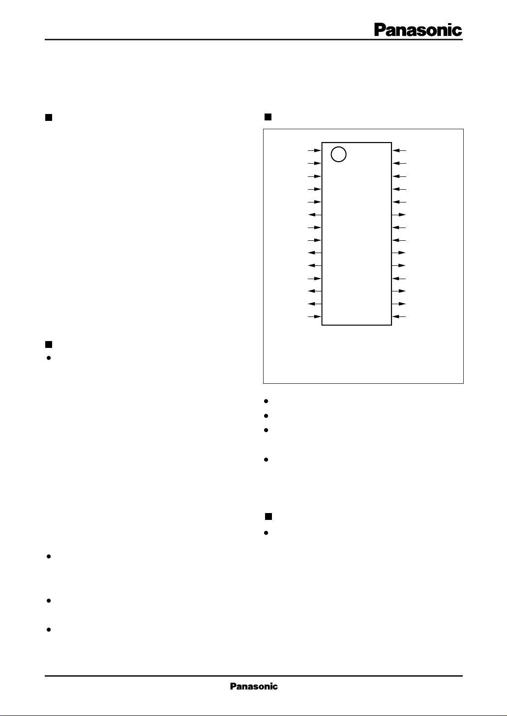
Pin Assignment
DIN
LRCK
BCK
M4
DV
DD2
CKO
DV
SS2
M1
OUT1C
OUT1B
AV
DD1
OUT1D
OUT1A
AV
SS1
s
8PEM output configuration (4PEM output per channel)
Support for low-voltage (3.3-volt) operation
Choice of system clocks:
192 f
Choice of input data formats: left-packed, rightpacked, I
MSB first)
1
2
3
4
5
6
7
8
9
10
11
12
13
14
28
27
26
25
24
23
22
21
20
19
18
17
16
15
(TOP VIEW)
SOP028-P-0375
, 256 fs, 384 fs, 512 fs, 576 f
s
2S
bus (16 or 20 bits, alternating channel input,
s
Applications
CD players and other digital audio equipment
RSBDN
RSBUP
M3
DV
DD1
XIN
XOUT
DV
SS1
M2
OUT2C
OUT2B
AV
DD2
OUT2D
OUT2A
AV
SS2
Page 2
MN35502 For Audio Equipment
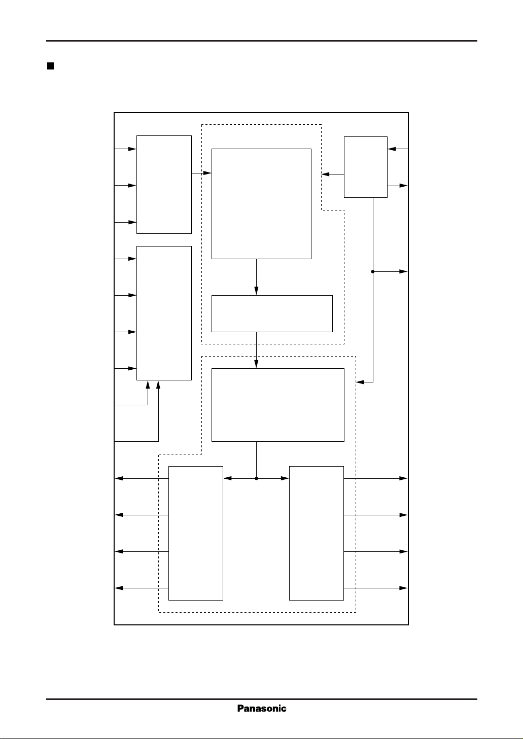
Block Diagram
DIN
LRCK
BCK
M1
M2
M3
M4
RSBDN
1
2
3
8
21
26
4
28
I/F
Block
Mode
Control
Block
DF Block
• De-emphasis
IIR Filter
• Attenuater
• 8fs
Over sampling
Digital Filter
1st. Order
Noise shaper Block
VANS
Noise shaper Block
OSC
Block
24
XIN
23
XOUT
6
CKO
RSBUP
OUT1C
OUT1B
OUT1D
OUT1A
27
9
10
PEM
12
13
Block
D/A Block
PEM
Block
20
OUT2C
19
OUT2B
17
OUT2D
16
OUT2A
Page 3
For Audio Equipment
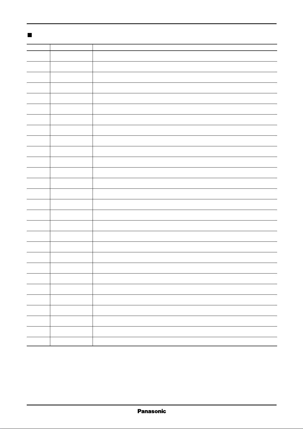
Pin Descriptions
Pin No. Pin Name Function Description
1 DIN Serial data pin (MSB first)
2 LRCK LR synchronization signal input pin (fs rate)
3 BCK Data shift bit clock input pin
4 M4 Operating mode selection pin 4 (See Table 1.)
MN35502
5DV
DD2
Power supply pin 2 for digital circuits
6 CKO Clock output pin
7DV
SS2
Ground pin for digital circuits
8 M1 Operating mode selection pin 1, with pull-up resistor (See Table 1.)
9 OUT1C PEM output pin 1C (Left channel with reversed phase)
10 OUT1B PEM output pin 1B (Left channel with same phase)
11 AV
DD1
Power supply pin 1 for analog circuits
12 OUT1D PEM output pin 1D (Left channel with reversed phase)
13 OUT1A PEM output pin 1A (Left channel with same phase)
14 AV
15 AV
SS1
SS2
Ground pin 1 for analog circuits
Ground pin 2 for analog circuits
16 OUT2A PEM output pin 2A (Right channel with same phase)
17 OUT2D PEM output pin 2D (Right channel with reversed phase)
18 AV
DD2
Power supply pin 2 for analog circuits
19 OUT2B PEM output pin 2B (Right channel with same phase)
20 OUT2C PEM output pin 2C (Right channel with reversed phase)
21 M2 Operating mode selection pin 2, with pull-up resistor (See Table 1.)
22 DV
SS1
Ground pin 1 for digital circuits (Ground for oscillator circuit)
23 XOUT Crystal oscillator pin
24 XIN Crystal oscillator pin (external clock input pin) (Built-in feedback resistor)
25 DV
DD1
Power supply pin 1 for digital circuits
26 M3 Operating mode selection pin 3, with pull-up resistor (See Table 1.)
27 RSBUP Reset pin/digital attenuation control pin (See Table 2.)
28 RSBDN Reset pin/digital attenuation control pin (See Table 2.)
Page 4
MN35502 For Audio Equipment
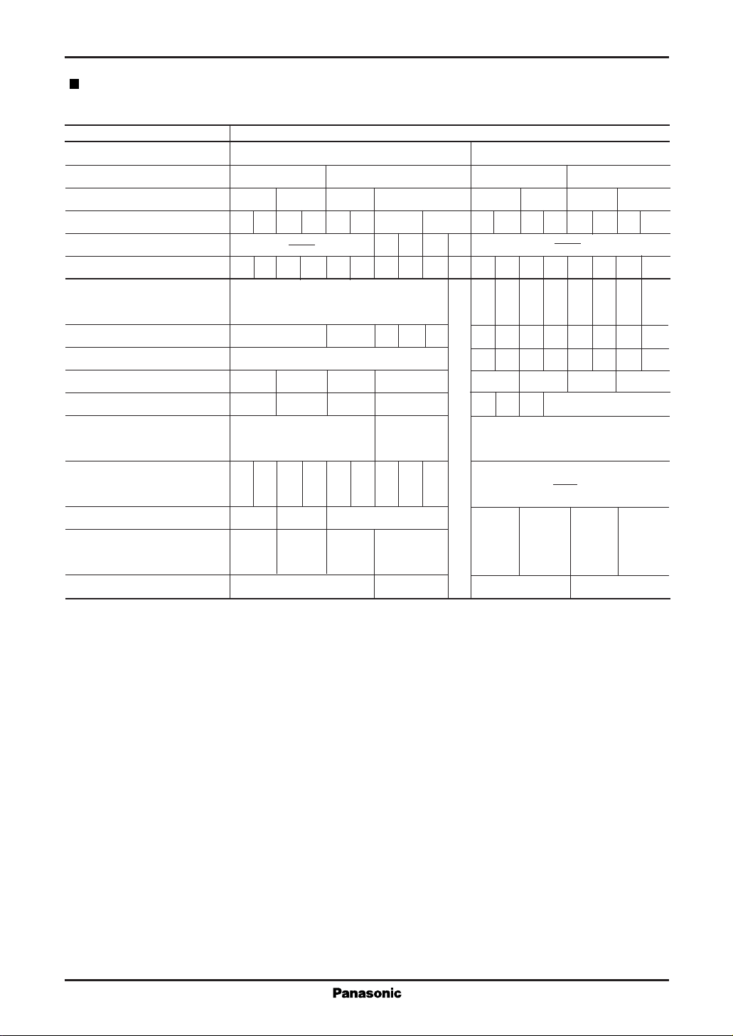
Operating Mode Descriptions
Table 1. MN35502 Operating Modes
Mode Selection Pins Pin States and Operating Modes
M1 L H
M2 L H H H
M3 LHL H LHLH
M4 LHLHLH L H LHLHLHLH
RSBUP L H L H
Mode 0123456061707189ABCDEF
2
Input data format Right-packed I
Right-
packed
Right-
packed
Left-
packed
Left-
packed
Input word length (bit) 16 20 16 20 16 16 20 16 20 16 20 16 20
Data when LRCK=H Left channel R L R L L R L R
XIN clock frequency (fs) 384 192 384 512 384 576 256 384
CKO output frequency (fs) 384 192 384 512 32 64 32 64
SI2S
Right-
packed
Right-
packed
Digital attenuation Available Not available Available
De-emphasis
—O—O—O——O
Test Mode
(fs=44.1kHz)
VANS oversampling (fs) 6432 64 64966496
Theoretical signal-to-noise
134 107 134 128 134 150 128 144
ratio (dB)
Output level 0.666 × AV
Notes
1: Modes 2 and 3 support f
2: Modes A, B, E, and F support f
clock speeds up to 88.2 kHz.
s
clock speeds up to 32 kHz; the others, up to 48 kHz.
s
DD
0.4995 × AV
DD
0.666 × AV
DD
0.4995 × AV
DD
Page 5
For Audio Equipment
MN35502
Functional Descriptions
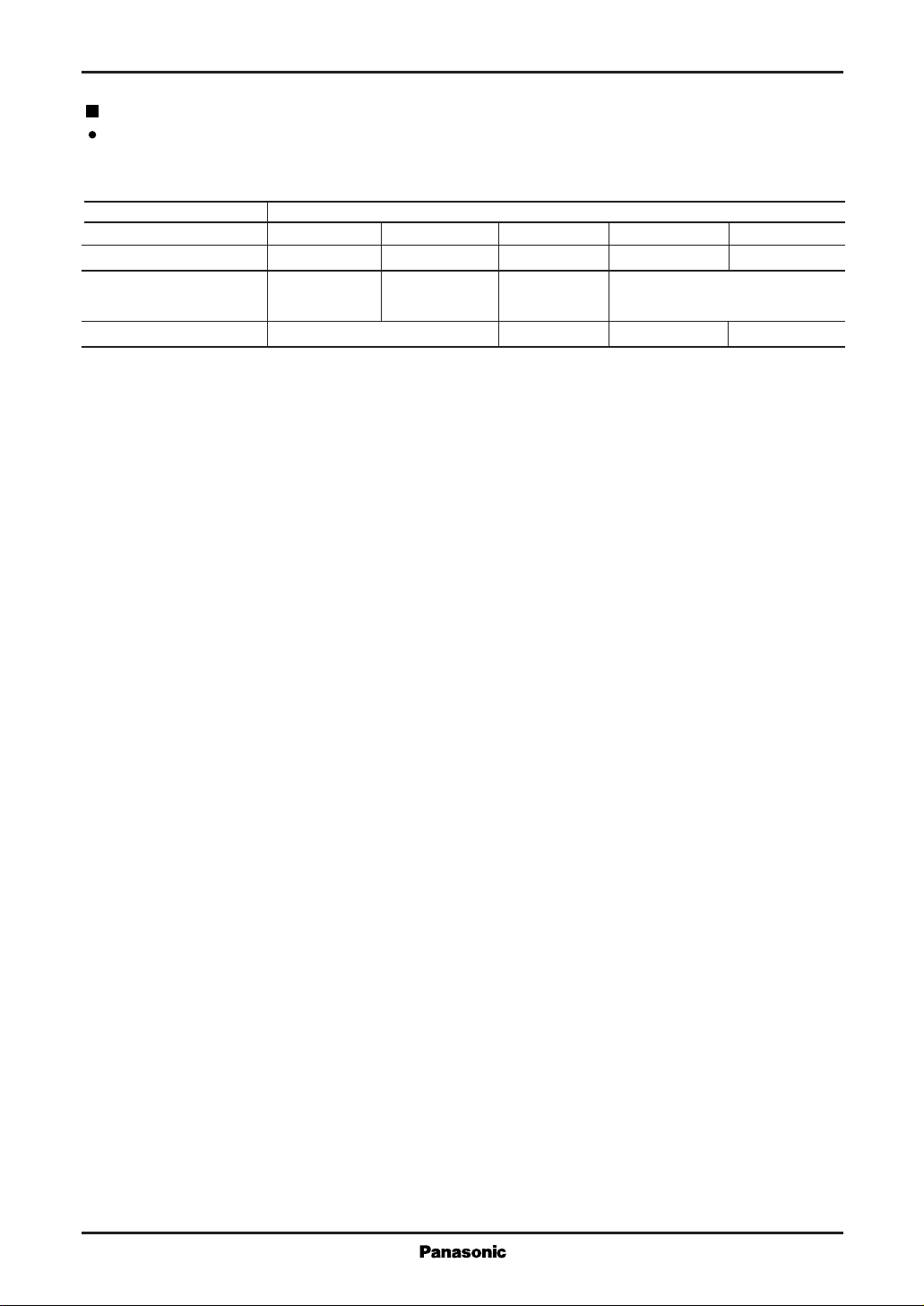
Digital attenuation and reset
Table 2 shows how the inputs from the two pins RSBUP and RSBDN control digital attenuation.
Table 2. Attenuation Modes
Pin Name Pin States and Operating Modes
RSBUP L ↑↓ L ↑ H
RSBDN L L ↑ H ↑
Mode Reset Mute Normal Attenuation control
Volume Mute (–∞) 0dB UP DOWN
Notes
1: The upw ard arrow indicates the rising edge change of the input signal; the paired arrows, the rising and falling edge changes.
2: Always reset the chip after applying the power, restarting the clock, or changing the clock speed. (Wait for the crystal
oscillation to stabilize and then apply a reset signal at least eight LRCK clock cycles long.)
3: Digital attenuation is not available for modes with a master clock of 512 fs (modes 60 to 70).
There are a total of 32 attenuation levels.
According to the attenuation control shown in Table-2, volume goes up or down in one step every input-signal
rising-edge. Still, in the 0 dB state, up-pulse does not change the volume. Similary, in the muting state (–∞), downpulse does not change the volume.
The change of the input signals is detected by inner clock of 32 f
for changes in the RSBUP and RSBDN signals.
Do not simultaneously change the RSBUP and RSBDN signals unless setting up for a reset.
period, so always use a frequency of 16 fs or less
s
Page 6
MN35502 For Audio Equipment
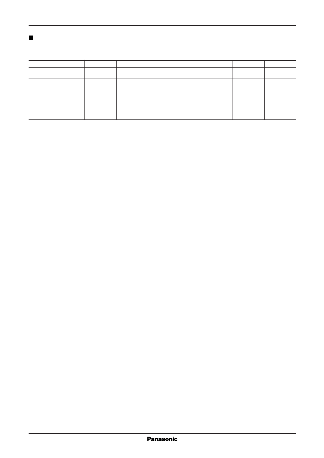
Conversion Characteristics
DVDD=5.0V, DVSS=0V, AVDD=5.0V, AVSS, f=16.9344MHz, Ta=25˚C
Analog Characteristics for 20-bit, 1 fs input
Parameter Symbol Test Condition min typ max Unit
Signal-to-noise ratio SN EIAJ (kHz) 114 dB
Dynamic range D.R. EIAJ (kHz) 113 dB
Total harmonic
distortion
Output level 1kHz F.S. 2.1 V
The above analog characteristics are based on measurements with the sample application circuit using mode 4.
THD+N EIAJ (kHz) 0.0006 0.0010 %
rms
Page 7
For Audio Equipment
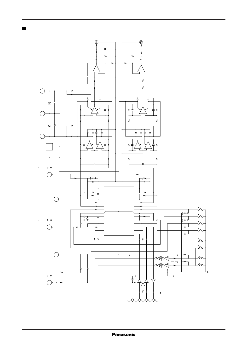
Application Circuit Example
MN35502
–12V
GND
+12V
OUT
78M05
0.1µF
DD
AV
DD
DV
5V
IN
GND
GND
0.1µF
0.1µF
18Ω
18Ω
18Ω
18Ω
18Ω
18Ω
100Ω
0.047µF
1.8kΩF 1.8kΩF
13kΩF
180Ω
Xtal
+
100µF
16.9344MHz
18Ω
+
47µF
0.022µFG
0.0015µF
+
47µF
330pFG
–
470µF
27kΩF
27kΩF
27kΩF
27kΩF
+
R ch.
+
0.047µF
+
330pF
+
1.5µF
1.5µF
560Ω
47µF
180Ω
0.0056µF
360Ω
47µF
–
+
0.0039µFG
510ΩF
560ΩF
0.047µF
–
0.047µF
+
560Ω
180Ω
27kΩ
4.7kΩ
0.0015µF
+
47µF
330pFG
–
180Ω
15
16
17
18
19
20
21
22
23
24
25
26
27
28
(
TOP VIEW
180Ω
1.8kΩF
1.8kΩF
13kΩF
AV
SS2
OUT2A
OUT2D
AV
DD2
OUT2B
OUT2C
M2
DV
SS1
XOUT
XIN
DV
DD1
M3
RSBUP
RSBDN
AV
OUT1A
OUT1D
AV
OUT1B
OUT1C
DV
DV
LRCK
)
0.047µF
0.0056µF
27kΩ
47kΩ
0.0039µFG
0.047µF
1.8kΩF
47µF
330pFG
13kΩF
180Ω
14
SS1
13
12
11
DD1
10
9
M1
8
7
SS2
CKO
6
5
DD2
M4
4
BCK
3
2
1DIN
1
GND
1.8kΩF
0.0015µF
+
–
100Ω
180Ω
47µF
–
560ΩF
–
0.047µF
+
330pF
470µF
27kΩF
1.5µF
27kΩF
560Ω
1.5µF
180Ω
560Ω
560Ω
560Ω
DATA
L ch.
360Ω
+
510ΩF
0.047µF
+
0.047µF
+
+
27kΩF
27kΩF
560Ω
560Ω
560Ω
560Ω
BCK
LRCK
0.022µFG
0.0015µF
47µF
+
330pFG
–
180Ω
+
10Ω
74HC14A
100Ω
CK
1.8kΩF
1.8kΩF
13kΩF
220µF
0.047µF
74HC4050
9
GND
0.1µF
100kΩ
0.1µF
100kΩ
11kΩ
11kΩ
11kΩ
11kΩ
M1
M2
M3
M4
RSBUP
RSBDN
UP
DOWN
Page 8
MN35502 For Audio Equipment
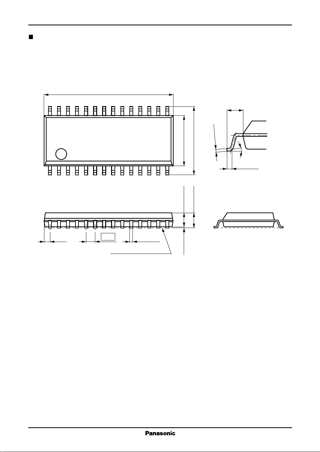
Package Dimensions (Unit: mm)
SOP028-P-0375
17.80
±0.20
28
15
0.05
-
+0.10
1.10±0.20
0.15
7.20±0.202.00±0.200.10±0.10
0 to 10°
0.30min.
114
2.40max. 9.40±0.30
(0.65) 0.40
1.27
±0.10
SEATING PLANE
 Loading...