

Page 1
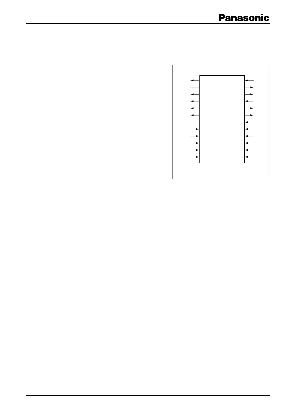
Video Camera IC
MN3114
Vertical Driver (8 channels) for CCD Area Image Sensors
■ Overview
The MN3114 is an 8-channel vertical driver for twodimensional interline CCD area image sensors that also
integrates a single SUB driver channel on the same chip.
Adoption of this IC can reduce both power consumption and parts counts in end products.
■ Features
•
Vertical driver block:
Consists of level shifters and 2-value/3-value output
driver circuits.
•
SUB driver block:
Consists of a level shifter and a 2-value output driver
circuit.
•
Package: 24-pin SSOP
■ Applications
•
Digital still cameras, video cameras
OSUB
VL
OV8
OV4
OV1
OV5
(N.C.)
VDC
CH3
IV1
CH1
IV4
1
2
3
4
5
6
7
8
9
10
11
12
(TOP VIEW)
24
23
22
21
20
19
18
17
16
15
14
13
VHH
OV6
OV2
VM
OV3
OV7
VH
CH4
IV3
CH2
IV2
ISUB
Preliminary
Publication date: April 2002 SDB00057AEM
1
Page 2
MN3114 Video Camera IC
■ Block Diagram
OSUB
VL
OV8
OV4
OV1
OV5
N.C.
VDC
1
2
3
4
5
6
7
8
3-value
driver
3-value
driver
3-value
driver
3-value
driver
Level
shifter
24
23
22
21
20
19
18
17
VHH
OV6
OV2
VM
OV3
OV7
VH
CH4
CH3
IV1
CH1
9
10
11
Level
shifter
Level
shifter
Level
shifter
Preliminary
12
IV4
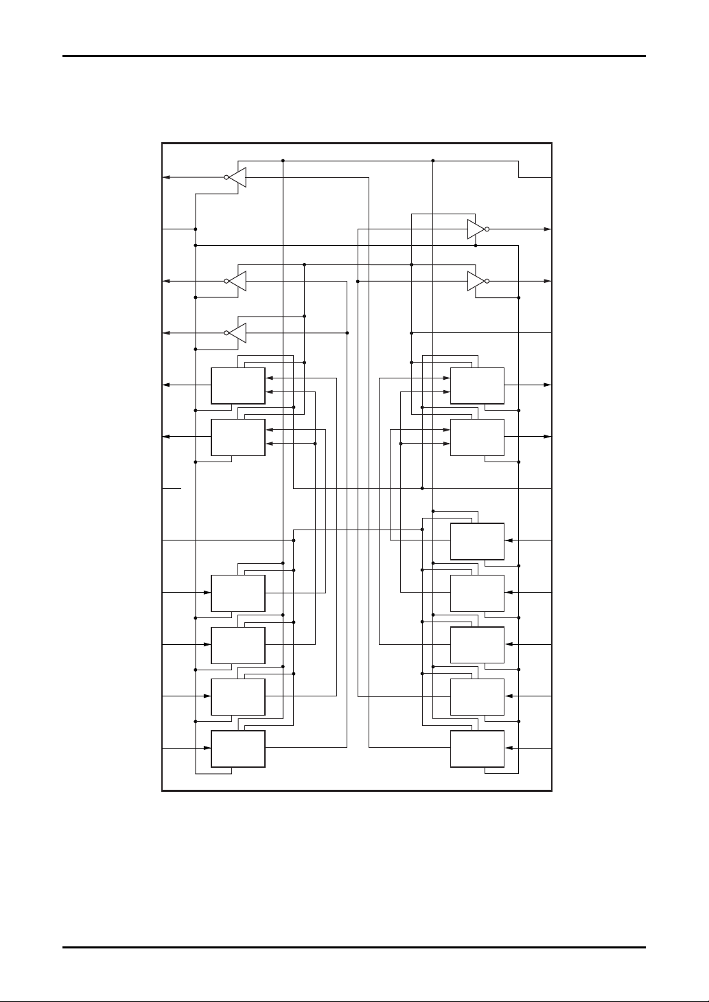
Note) VDC, VL, and VM: Common power supply
VHH and VH: SUB driver block and vertical driver 3-value independent power supply
2
Level
shifter
SDB00057AEM
Level
shifter
Level
shifter
Level
shifter
Level
shifter
16
15
14
13
IV3
CH2
IV2
ISUB
Page 3
Video Camera IC MN3114
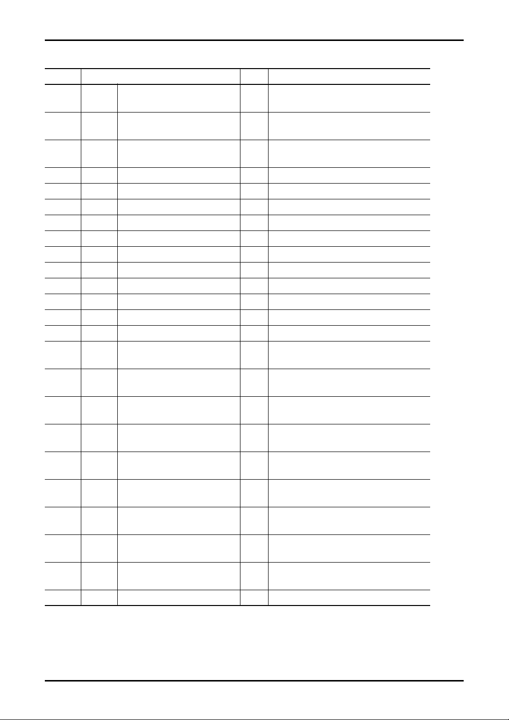
■ Pin Descriptions
Pin No. Pin name I/O Description
8 VDC Input block I Low-voltage system high-level input
high-level supply voltage
18 VH Vertical driver block I High-voltage system high-level input
high-level supply voltage
24 VHH SUB driver block I High-voltage system high-level input
high-level supply voltage
21 VM Middle-level supply voltage I High-voltage system middle-level input
2 VL Low-level supply voltage I High-voltage system low-level input
10 IV1 Transfer pulse input I Charge transfer pulse input
14 IV2 Transfer pulse input I Charge transfer pulse input
16 IV3 Transfer pulse input I Charge transfer pulse input
12 IV4 Transfer pulse input I Charge transfer pulse input
11 CH1 Charge pulse input I Charge readout pulse input
15 CH2 Charge pulse input I Charge readout pulse input
9 CH3 Charge pulse input I Charge readout pulse input
17 CH4 Charge pulse input I Charge readout pulse input
13 ISUB SUB pulse input I Unneeded charge sweep-out pulse input
5 OV1 3-value transfer pulse O 3-value transfer pulse output
output (VH, VM, or VL)
22 OV2 2-value transfer pulse O 2-value transfer pulse output
output (VH or VL)
20 OV3 3-value transfer pulse O 3-value transfer pulse output
output (VH, VM, or VL)
4 OV4 2-value transfer pulse O 2-value transfer pulse output
output (VH or VL)
6 OV5 3-value transfer pulse O 3-value transfer pulse output
output (VH, VM, or VL)
23 OV6 2-value transfer pulse O 2-value transfer pulse output
output (VH or VL)
19 OV7 3-value transfer pulse O 3-value transfer pulse output
3 OV8 2-value transfer pulse O 2-value transfer pulse output
1 OSUB SUB pulse output O Unneeded charge sweep-out pulse output
7 N.C.
Preliminary
output (VH, VM, or VL)
output (VH or VL)
(VHH or VL)
SDB00057AEM
3
Page 4
MN3114 Video Camera IC
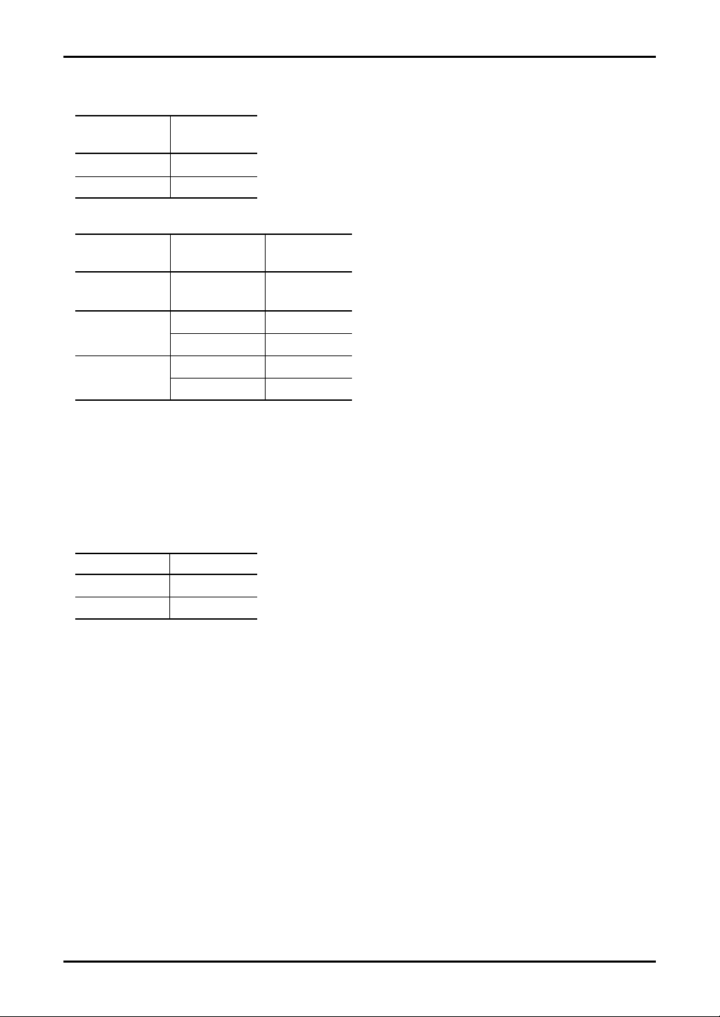
■ Operating Mode Table
1. 2-value transfer pulse (vertical driver block)
IV2 OV2, OV6
IV4 OV4, OV8
High Low
Low Mid
2. 3-value transfer pulse
CH1 IV1 OV1
CH2 IV3 OV3
CH3 IV1 OV5
CH4 IV3 OV7
High High Low
Low Mid
Low High Low
Low High
Note) IV1, IV2, IV3, IV4, CH1, CH2
High: VDC
Low: GND
OV1, OV2, OV3, OV4, OV5, OV6, OV7, OV8
High: VH
Mid: VM
Low: VL
3. Unneeded charge sweep-out pulse (SUB driver block)
ISUB OSUB
High Low
Low High
Note) ISUB
High: VDC
Low: GND
OSUB
High: VHH
Low: VL
Preliminary
4
SDB00057AEM
Page 5
Video Camera IC MN3114
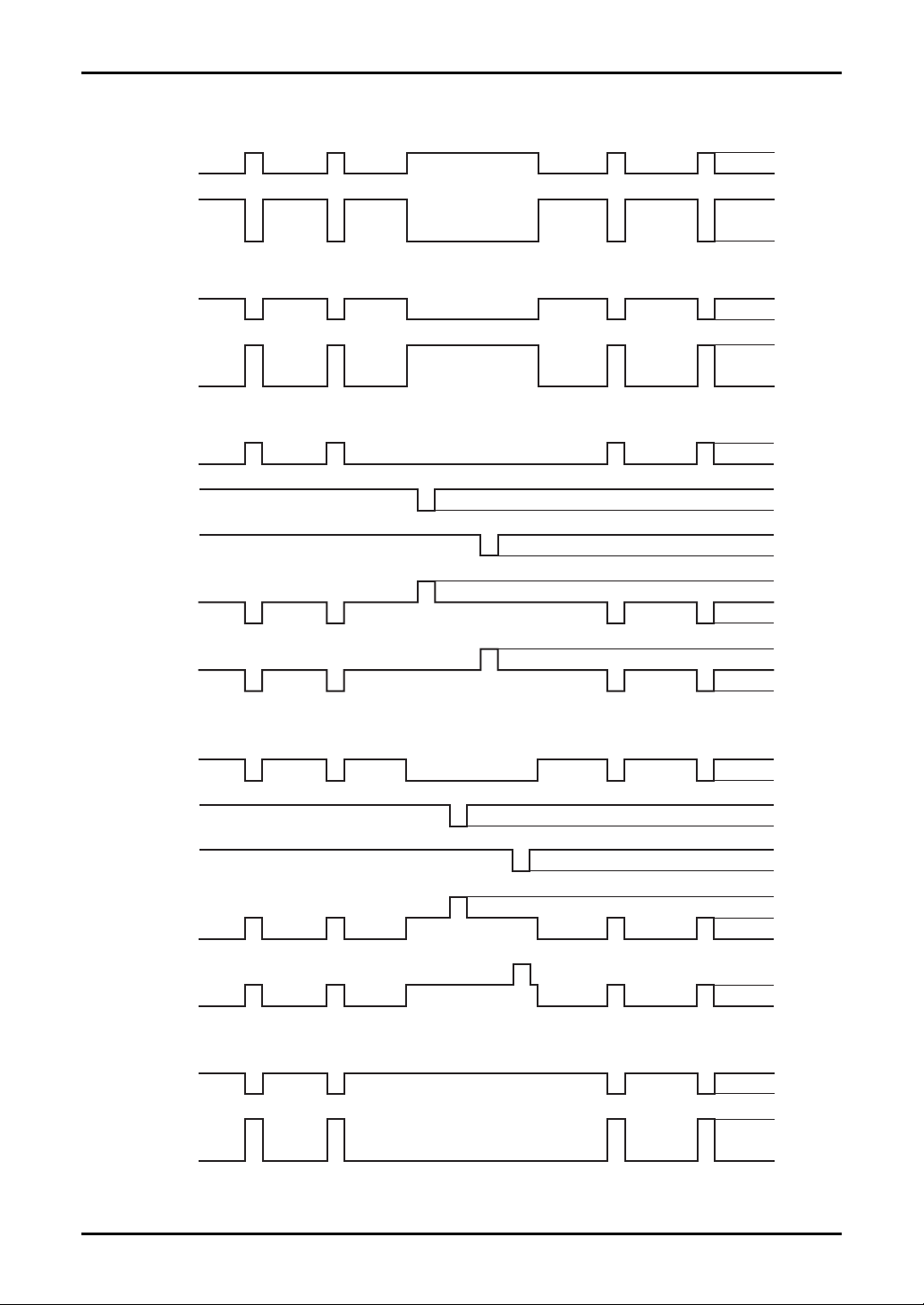
■ Timing Charts
1. 2-value transfer pulse
IV2
OV2, OV6
2. 2-value transfer pulse
IV4
OV4, OV8
High
Low
Mid
Low
High
Low
Mid
Low
3. 3-value transfer pulse
IV1
CH1
CH3
OV1
OV5
4. 3-value transfer pulse
IV3
CH2
CH4
OV3
OV7
High
Low
High
Low
High
Low
High
Mid
Low
High
Mid
Low
High
Low
High
Low
High
Low
High
Mid
Preliminary
Low
High
Mid
Low
5. SUB pulse
ISUB
OSUB
SDB00057AEM
High
Low
High
Low
5
Page 6
MN3114 Video Camera IC
■ Electrical Characteristics
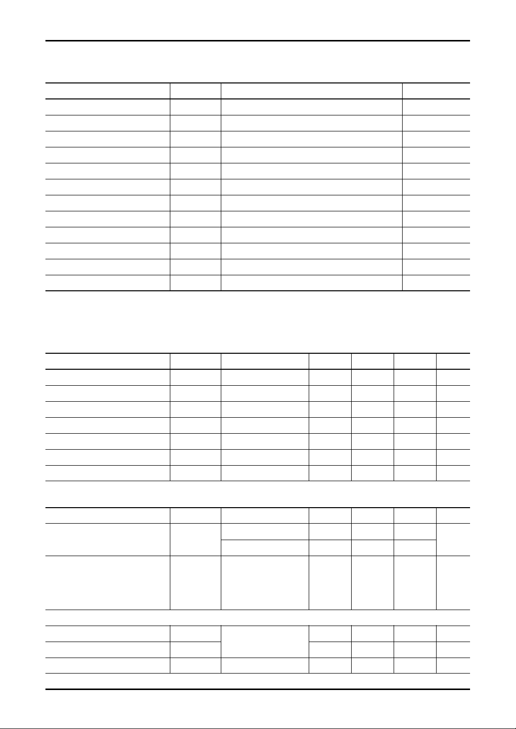
1. Absolute Maximum Ratings
Parameter Symbol Rating Unit
Supply voltage 1 VHH-VL 33 V
Supply voltage 2 VH-VL 30 V
Supply voltage 3 VM VL to 6 V
Supply voltage 4 VDC 0 to 5 V
Negative supply voltage VL −12 to 0 V
Input voltage VI VL− 0.3 to VDC+0.3 V
Input and output clamp diode current
Maximum DC load current IODC ±3mA
Maximum load capacitance CL (5 500)
Power dissipation PD (180)
Operating temperature Topr −20 to +75 °C
Storage temperature Tstg −50 to +125 °C
Note) 1. The absolute maximum ratings are limit values for stresses applied to the chip so that the chip will not be destroyed.
Operation is not guaranteed within these ranges.
2.*: Preliminary values
IIC, IOC ±10 mA
*
*
pF/pin
mW
2. Operating Conditions at Ta = −20°C to +75°C
Parameter Symbol Condition Min Typ Max Unit
Negative supply voltage VL −10 −4V
Supply voltage 1 VDC 2.7 3.6 V
Supply voltage 2 VHH-VL VH-VL 31 V
Supply voltage 3 VH-VL 28 V
Supply voltage 4 VHH-VM 15 18 V
Supply voltage 5 VM V
Input frequency fIN 500 kHz
3. DC Characteristics at VHH = 15.0 V, VH = 15.0 V, VL = −7.5 V, VDC = 2.7 V to 3.6 V, Ta = −20°C to +75°C
Parameter Symbol Condition Min T yp Max Unit
Quiescent supply current IDDST mA
Operating supply current IDDDYN ■ Test conditions (7)
1) Input pins: IV1, IV2, IV3, IV4, CH1, CH2, CH3, CH4, ISUB
High-level voltage VIH VDC = 3.0 V VDC × 0.7 VDC V
Low-level voltage VIL 0.0 VDC × 0.3 V
Input leakage current IILK VI = 0 to VDC (−1.0)
Note)*: Preliminary values
6
Preliminary
VI = GND, VDC = 3.0 V
See 2. Input pulse
timing chart.
VI = GND or VDC
SDB00057AEM
(5)
*
(1.0)
*
*
mA
*
µA
Page 7
Video Camera IC MN3114
■ Electrical Characteristics (continued)
3.
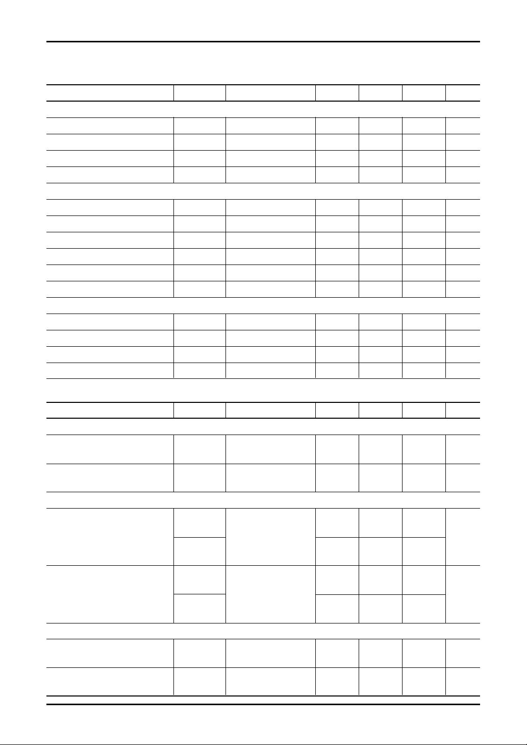
DC Characteristics (continued) at VHH = 15.0 V, VH = 15.0 V, VL = −7.5 V, VDC = 2.7 V to 3.6 V, Ta = −20°C to +75°C
Parameter Symbol Condition Min Typ Max Unit
2) Output pins 1 (2-value output): OV2, OV4, OV6, OV8
Mid-level output voltage VOM1 IOM1 = −1 mA − 0.1 VM V
Low-level output voltage VOL1 IOL1 = 1 mA VL −7.4 V
Mid-level output on resistance RONM1 IOM1 = −50 mA 40 Ω
Low-level output on resistance RONL1 IOL1 = 50 mA 30 Ω
3) Output pins 2 (3-value output): OV1, OV3, OV5, OV7
High-level output voltage VOH2 IOH2 = 1 mA 14.9 VH V
Mid-level output voltage VOM2 IOM2 = 1 mA − 0.1 VM V
Low-level output voltage VOL2 IOL2 = 1 mA VL −7.4 V
Output on resistance (high level) RONH2 IOH2 = 50 mA 40 Ω
Output on resistance (mid level) RONM2 IOM2 = ±50 mA 30 Ω
Output on resistance (low level) RONL2 IOL2 = 50 mA 30 Ω
4) Output pins 3 (SUB output): OSUB
High-level output voltage VOHH3 IOHH3 = −1 mA 14.9 VHH V
Low-level output voltage VOL3 IOL3 = 1 mA VL −7.4 V
Output on resistance (high level) RONHH3 IONHH3 = −50 mA 40 Ω
Output on resistance (low level) RONL3 IOL3 = 50 mA 30 Ω
4. AC Characteristics at VHH = 15.0 V, VH = 15.0 V, VL = −7.5 V, VDC = 2.7 V to 3.6 V, Ta = −20°C to +7 5°C
Parameter Symbol Condition Min T yp Max Unit
1) Output pins 1 (2-value output): OV2, OV4, OV6, OV8
Transmission delay time TPLM No load 100 200 ns
TPML
Rise time TTLM 200 300 ns
Fall time TTML
2) Output pins 2 (3-value output): OV1, OV3, OV5, OV7
Transmission delay time TPLM No load 100 200 ns
Preliminary
Rise time TTLM 200 300 ns
Fall time TTML
3) Output pins 3 (SUB output): OSUB
Transmission delay time TPLHH No load 100 200 ns
Rise time TTLHH 200 300 ns
Fall time TTHHL
TPML
TPMH 100 200
TPHM
TTMH 200 300
TTHM
TPHHL
SDB00057AEM
7
Page 8
MN3114 Video Camera IC
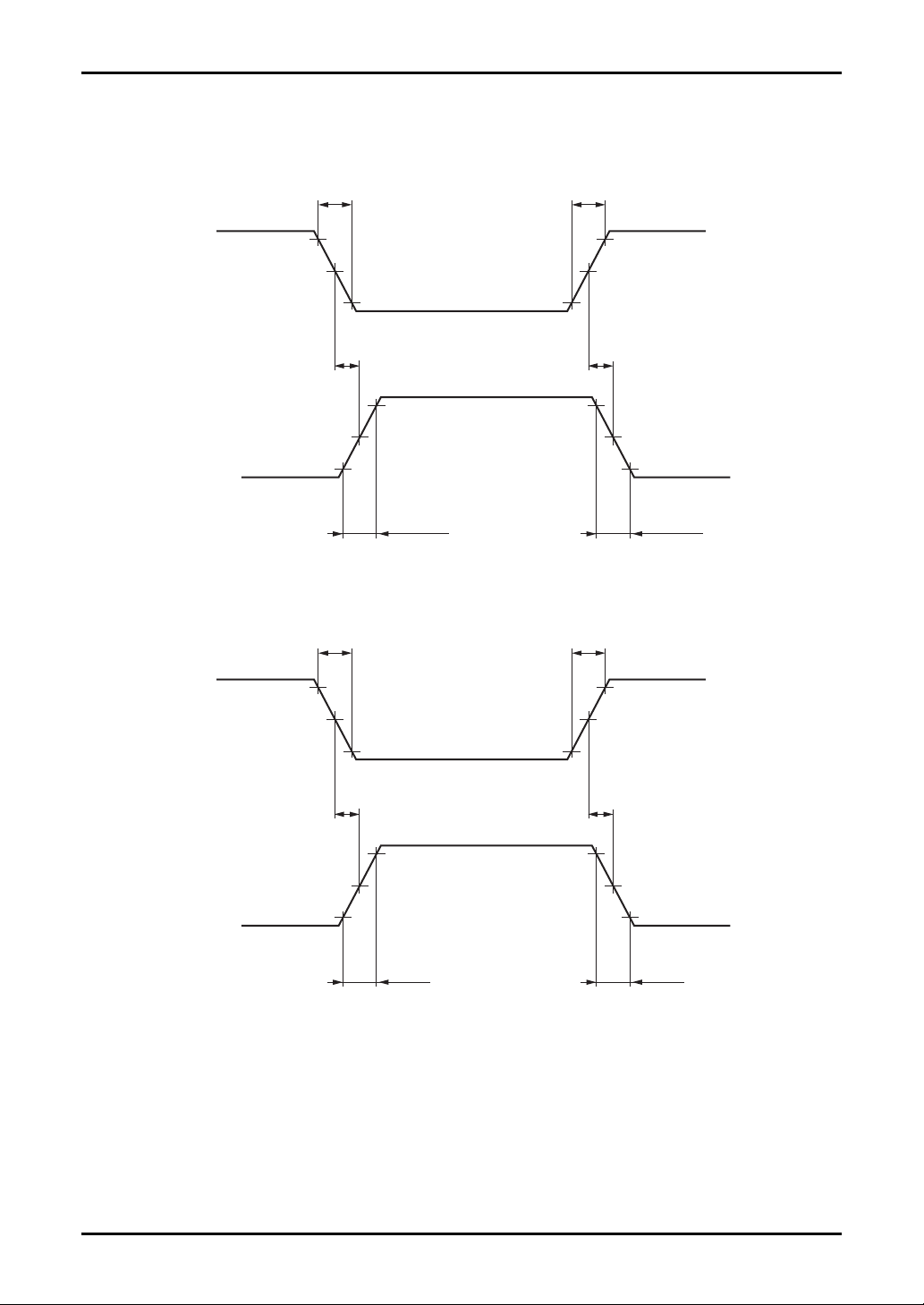
■ Test Conditions
1. Transmission delay time, rise time, and fall time
Input
IV1, IV2,
IV3, IV4,
(ISUB)
Output
OV1, OV2,
OV3, OV4,
OV5, OV6,
OV7, OV8,
(OSUB)
Input
CH1, CH2,
CH3, CH4
*
tf
TPLM
(TPLHH)
*
tf
90%
50%
10%
90%
50%
10%
TTLM
(TTLHH)
90%
50%
10%
*
tr
TPML
(TPHHL)
*
tr
TTML
(TTHHL)
VDC
GND
VDC
GND
VOM
(VOHH)
VOL
(VOL)
Output
OV1, OV3,
OV5, OV7
Note) *: tr = tf = 20 ns (typ.)
8
TPMH TPHM
90%
50%
10%
Preliminary
TTMH TTHM
SDB00057AEM
VOH
VOM
Page 9
Video Camera IC MN3114
■ Test Conditions (continued)
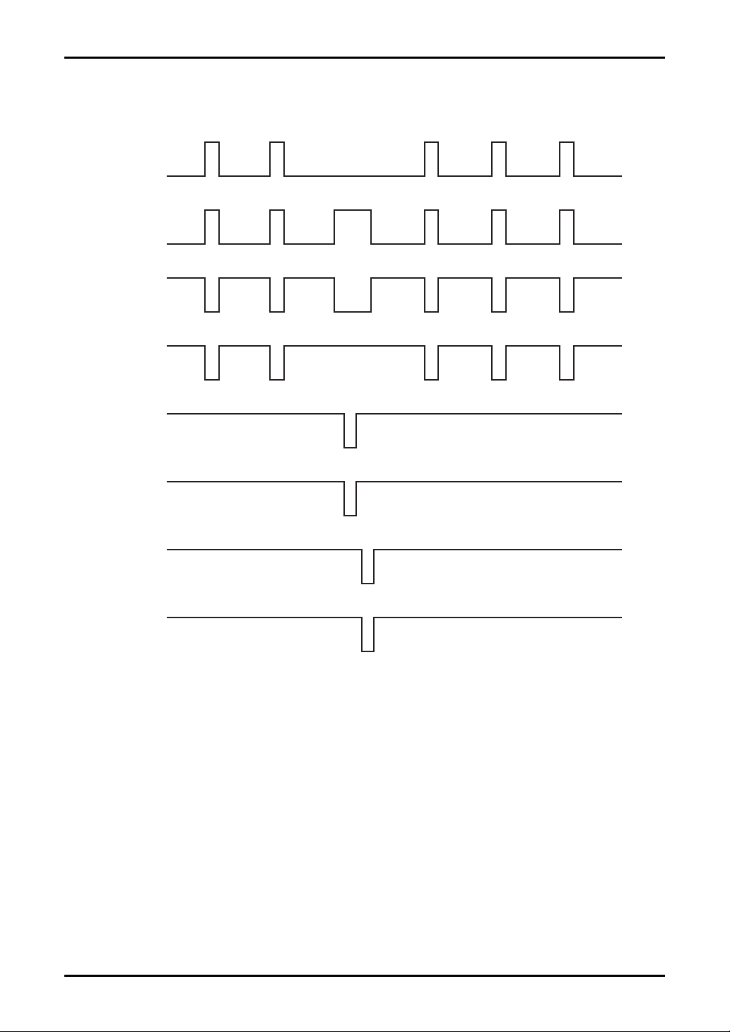
2. Input pulse timing chart
IV1
IV2
IV3
IV4
CH1
CH2
CH3
CH4
■ Usage Notes
1. If the SUB driver is not used:
1) Connect VHH to VH.
2) Connect ISUB to VDC.
3) Leave OSUB (pin 1) open.
2. Connect bypass condensers to the MN3114 power supply pins VHH, VH, VM, VL, and VDC. Locate these bypass
condensers as close to the IC as possible.
3. Guarantee period after opening the sealed packing:
The guarantee period after opening the sealed desiccated packing is three weeks under environment temperature and
humidity conditions of 30°C and 70% RH.
4. The recommended reflow temperature is 230°C.
Preliminary
SDB00057AEM
9
Page 10
MN3114 Video Camera IC
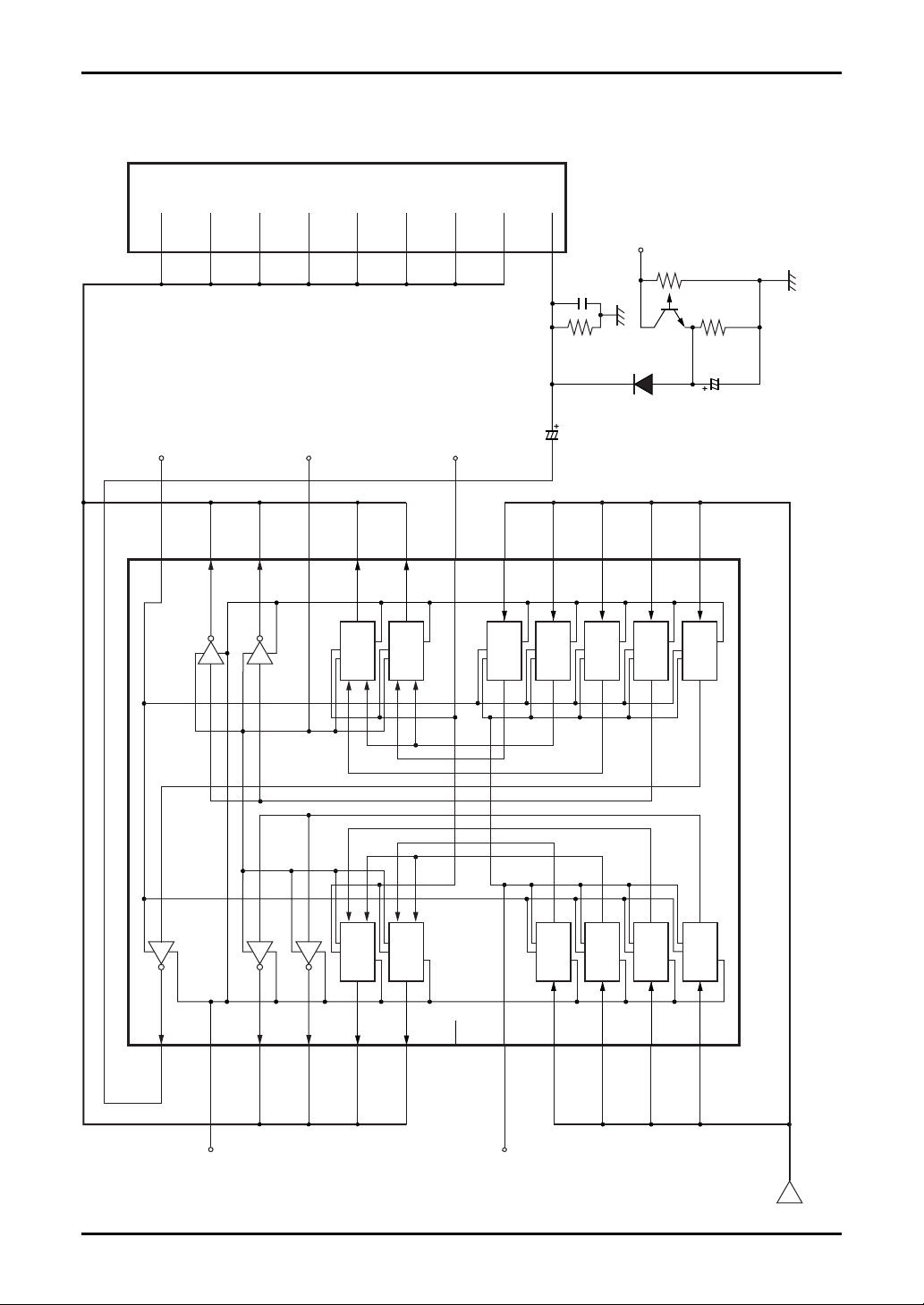
■ Application Circuit Example
CCD
V1
V2
V3
V4
V5
V6
V7
V8
SUB
200 pF
2
+16 V
200 kΩ
VHH
VHH
24
OV6
23
OV2
22
VM
21
VM
OV3
20
3-value
1 MΩ
VH
VH
OV7
18
19
driver
driver
3-value
CH4
17
Level
shifter
3.3 µF / 5 V
IV3
16
Level
shifter
CH2
15
Level
shifter
IV2
14
Level
shifter
ISUB
13
Level
shifter
47 kΩ
3.3 µF / 50 V
10
1
OSUB
2
VL
Preliminary
Level
Level
Level
11
CH1
shifter
Level
12
IV4
shifter
VL
driver
3-value
3
4
5
OV4
OV8
OV1
driver
3-value
7
6
N.C.
OV5
SDB00057AEM
8
VDC
VDC
9
CH3
shifter
shifter
10
IV1
Note) Connect bypass condensers to the MN3114 power supply pins VHH, VH, VM, VL, and VDC.
Signal generator
Locate these bypass condensers as close to the IC as possible.
Page 11
Video Camera IC MN3114
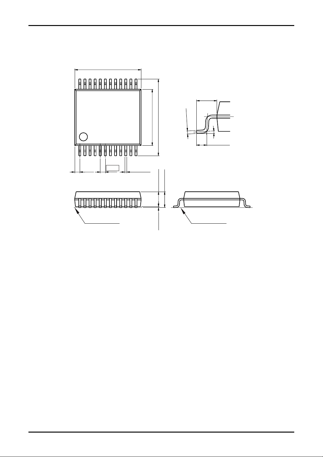
■ Package Dimensions (unit: mm)
• SSOP024-P-0300C (Lead-free package)
6.50±0.20
24
13
5.50±0.20
7.50±0.20
0.05
-
+0.10
0.15
1.00±0.20
0° to 10°
0.50±0.20
1
(0.50)
Seating plane
0.50
0.20
12
+0.10
-
0.05
1.50±0.20
0.10±0.10
1.60±0.30
Seating plane
Preliminary
SDB00057AEM
11
Page 12
Request for your special attention and precautions in using the technical information
and semiconductors described in this material
(1) An export permit needs to be obtained from the competent authorities of the Japanese Govern-
ment if any of the products or technologies described in this material and controlled under the
"Foreign Exchange and Foreign Trade Law" is to be exported or taken out of Japan.
(2) The technical information described in this material is limited to showing representative character-
istics and applied circuit examples of the products. It does not constitute the warranting of industrial
property, the granting of relative rights, or the granting of any license.
(3) The products described in this material are intended to be used for standard applications or gen-
eral electronic equipment (such as office equipment, communications equipment, measuring instruments and household appliances).
Consult our sales staff in advance for information on the following applications:
• Special applications (such as for airplanes, aerospace, automobiles, traffic control equipment,
combustion equipment, life support systems and safety devices) in which exceptional quality and
reliability are required, or if the failure or malfunction of the products may directly jeopardize life or
harm the human body.
• Any applications other than the standard applications intended.
(4) The products and product specifications described in this material are subject to change without
notice for reasons of modification and/or improvement. At the final stage of your design, purchasing, or use of the products, therefore, ask for the most up-to-date Product Standards in advance to
make sure that the latest specifications satisfy your requirements.
(5) When designing your equipment, comply with the guaranteed values, in particular those of maxi-
mum rating, the range of operating power supply voltage and heat radiation characteristics. Otherwise, we will not be liable for any defect which may arise later in your equipment.
Even when the products are used within the guaranteed values, redundant design is recommended,
so that such equipment may not violate relevant laws or regulations because of the function of our
products.
(6) When using products for which dry packing is required, observe the conditions (including shelf life
and after-unpacking standby time) agreed upon when specification sheets are individually exchanged.
(7) No part of this material may be reprinted or reproduced by any means without written permission
from our company.
Please read the following notes before using the datasheets
A. These materials are intended as a reference to assist customers with the selection of Panasonic
semiconductor products best suited to their applications.
Due to modification or other reasons, any information contained in this material, such as available
product types, technical data, and so on, is subject to change without notice.
Customers are advised to contact our semiconductor sales office and obtain the latest information
before starting precise technical research and/or purchasing activities.
B. Panasonic is endeavoring to continually improve the quality and reliability of these materials but
there is always the possibility that further rectifications will be required in the future. Therefore,
Panasonic will not assume any liability for any damages arising from any errors etc. that may appear in this material.
C. These materials are solely intended for a customer's individual use.
Therefore, without the prior written approval of Panasonic, any other use such as reproducing,
selling, or distributing this material to a third party, via the Internet or in any other way, is prohibited.
2001 MAR
 Loading...