

Page 1
For Video Equipment
MN3113F
Vertical Driver LSI for Video Camera CCD Area Image Sensor
Overview
The MN3113F is a vertical driver LSI for a two-dimensional interline CCD image sensor. It features a built-in
power supply circuit that, in conjunction with such
external components as six booster capacitors and two
voltage stabilization capacitors, produces stabilized
+15.0V and –10.0V power supplies from a +5.0V input
and HD pulses.
The MN3113F makes it possible to drive a CCD image
sensor on a single 5 volt power supply.
Features
Single 5 volt power supply
Adjustable output voltage for regulated voltage
circuit
Applications
Video cameras
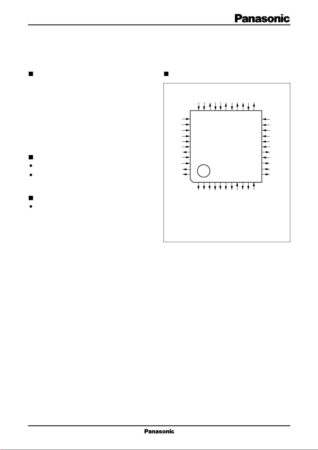
Pin Assignment
EEVHH
V
3332313029282726252423
IV1
IV3
IN –
C1+
C3+
34
35
36
37
38
39
40
41
42
43
44
1234567891011
C1–
ISUB
CH1
CH2
SENSE2
V
OUT–
V
GND
OSUB
VL2VL1OV1
V
C3 –
C4 –
C5 –
EE
OV
C6 –
C2–
(TOP VIEW)
QFP044-P-1010
M13
OV3
CC1
V
OV2
C6+
M24
V
DD
OV
OV4
22
21
20
19
18
17
16
15
14
13
12
HD
V
H
V
DD
V
CC2
IV2
IV4
SENSE1
V
OUT+
V
IN+
CAP3
CAP2
CAP1
Page 2
MN3113F For Video Equipment
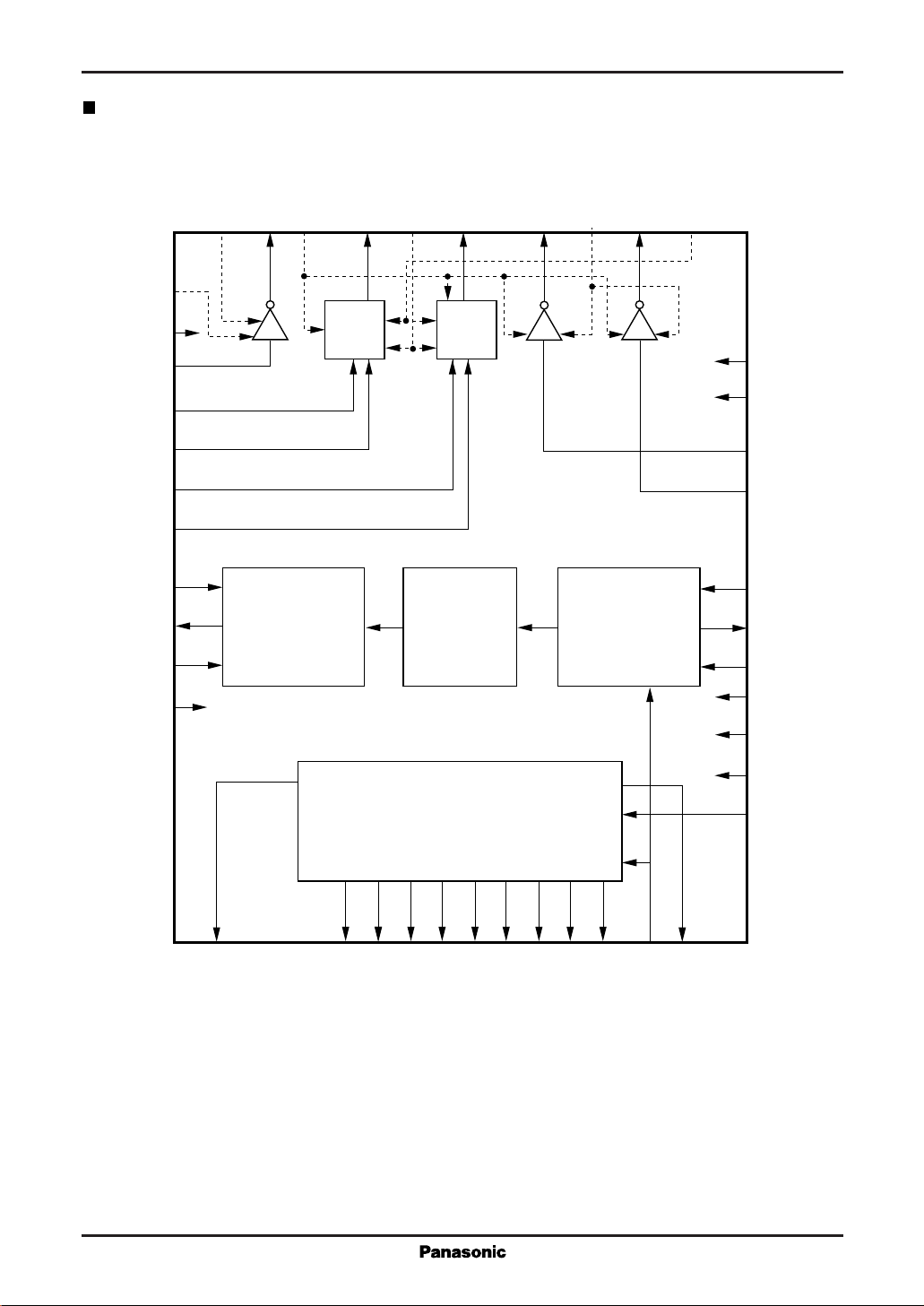
Block Diagram
VL2
V
ISUB
IV1
CH1
IV3
CH2
SENSE2
V
OUT–
V
IN –
GND
HH
V
31
32
OSUB28V
29
L1
OV126V
27
M13
OV3
25
OV2
M24
V
24
23
OV4
H
V
22
30
33
EE
34
36
35
37
Tristate
driver
Tristate
driver
21
V
DD
20
V
CC2
19
IV2
18
IV4
38
39
40
Negative regulated
voltage output
Inverter circuit
Positive regulated
voltage output
41
42
Negative and positive boosting voltage generator
16
15
14
13
12
11
17
SENSE1
V
OUT+
V
IN+
CAP3
CAP2
CAP1
HD
6
EE
OV
1
–
C1
2
–
3
–
C2
43
+
C1
C3
4
5
C4
7
–
C5 –C6
44
–
+
C3
8
V
CC1
10
DD
OV
9
+
C6
Page 3
For Video Equipment MN3113F
Pin Descriptions
Pin No. Symbol Pin Name I/O Function Description
8V
20 V
CC1
CC2
42 GND "L" level power supply I "L" level input for 5 volt circuits
22 V
32 V
27 V
24 V
29 V
30 V
21 V
33 V
15 V
41 V
H
HH
M13
M24
L1
L2
DD
EE
IN+
IN –
11 HD HD pulse input I HD pulse input pin
19 IV2 Transfer pulse input I Charge transfer pulse input pin
18 IV4 Transfer pulse input I Charge transfer pulse input pin
36 IV1 Transfer pulse input I Charge transfer pulse input pin
37 IV3 Transfer pulse input I Charge transfer pulse input pin
35 CH1 Charge pulse input I Charge readout pulse input pin
38 CH2 Charge pulse input I Charge readout pulse input pin
34 ISUB SUB pulse input I Unwanted charge rejection pulse input pin
17 SENSE1 Positive voltage sensing I Positive voltage control sensing pin
39 SENSE2 Negative voltage sensing I Negative voltage control sensing pin
43 C1+ C1 connection O Booster block voltage charging capacitor
1 C1– connection pins
2 C2+ C2 connection O Booster block voltage charging capacitor
C2– connection pins
44 C3+ C3 connection O Booster block voltage charging capacitor
3 C3 – connection pins
4 C4 – C4 connection O Booster block voltage charging capacitor
5 C5 – C5 connection O Booster block voltage charging capacitor
"H" level power supply I "H" level input for 5 volt circuits
for input block
for input block
"H" level power supply I "H" level input for high-voltage circuits
for vertical driver
"H" level power supply I "H" level input for high-voltage circuits
for SUB driver
"M" level power supply I "M" level input for high-voltage circuits
for vertical driver
"L" level power supply I "L" level input for high-voltage circuits
for vertical driver
"L" level input I "L" level input for high-voltage circuits
for SUB driver
Power supply 1 for driver I "H" level for high-voltage circuits
Power supply 2 for driver I "L" level for high-voltage circuits
Positive regulated voltage I Positive regulated voltage block
block voltage input voltage input pin
Negative regulated voltage I Negative regulated voltage block
block voltage input voltage input pin
input
input
connection pins
connection pins
Page 4
MN3113F For Video Equipment
Pin Descriptions (continued)
Pin No. Symbol Pin Name I/O Function Description
7 C6 – C6 connection pins O Booster block voltage charging capacitor
9 C6+ connection pins
10 OV
6OV
16 V
40 V
DD
EE
OUT+
OUT–
23 OV4 Binary transfer pulse O Binary (V
25 OV2 Binary transfer pulse O Binary (V
26 OV3 Tristate transfer pulse O Tristate (V
28 OV1 Tristate transfer pulse O Tristate (V
31 OSUB SUB pulse output O Unwanted charge (V
12 CAP1 Stabilizing capacitor O Pins for connecting capacitors for internal
13 CAP2 connection voltage stabilization circuits
14 CAP3
Booster block positive O Booster block positive voltage output pin
voltage output
Booster block negative O Booster block negative voltage output pin
voltage output
Positive regulated voltage O Positive regulated voltage output pin
output
Negative regulated voltage O Negative regulated voltage output pin
output
, VL1) transfer pulse
M24
output output pin
, VL1) transfer pulse
M24
output output pin
, V
H
, VL1) transfer pulse
M13
output output pin
, V
H
, VL1) transfer pulse
M13
output output pin
, VL2) rejection
HH
pulse input pin
Page 5

For Video Equipment MN3113F
Functional Description
Binary transfer pulses (vertical driver block)
IV2 OV2
IV4 OV4
HL
LM
Tristate transfer pulses (vertical driver block)
CH1 IV1 OV1
CH2 IV3 OV3
H
L
1
*
IV1, IV2, IV3, IV4, CH1, CH2
H: V
CC
L: GND
OV1, OV2, OV3, OV4
H: V
H
M: V
, or V
L: V
M13
L1
M24
HL
LM
HL
LH
Unwanted charge rejection pulses (SUB driver block)
ISUB OSUB
HL
LH
1
*
ISUB
H: V
CC
L: GND
OSUB
H: V
HH
L: V
L2
Page 6

MN3113F For Video Equipment
Electrical Characteristics
(1) DC characteristics
VHH=VH=15.0V , V
V
CC1=VCC2
M13=VM24
=5.0V (=VCC), VL1 =–7.0V , VL2 =–10.0V , Ta=+25˚C
Parameter Symbol Test conditions min typ max Unit
Quiescent supply current I
Operating supply current I
Power supply output pins OV
Positive voltage stabilization V
circuit output voltage f
Negative voltage stabilization V
circuit output voltage f
Input pins IV1 , IV2 , IV3 , IV4 , CH1 , CH2 , ISUB , HD
"H" level voltage V
"L" level voltage V
Input leak current I
Output pins 1 (Binary output) OV2 , OV4
Output voltage "M" level V
Output voltage "L" level V
Output on resistance "M" level R
Output on resistance "L" level R
Output pins 2 (Tristate output) OV1 , OV3
Output voltage "H" level V
Output voltage "M" level V
Output voltage "L" level V
Output on resistance "H" level R
Output on resistance "M" level R
Output on resistance "L" level R
Output pin 3 (SUB output) OSUB
Output voltage "H" level V
Output voltage "L" level V
Output on resistance "H" level R
Output on resistance "L" level R
=1.0V , GND=0.0V ,
DDST
DDDYNVI
OUT+
OUT–
ONM1IOM1
ONL1IOL1
ONH2IOH2
ONM2IOM2
ONL2IOL2
OHH3
ONHH3IONHH3
ONL3IONL3
VI=GND , V
DD
VI=GND , VCC , IO=7mA 14.5 15.0 15.5 V
VI=GND , V
IH
IL
VI=0 to 5V ±1 µ A
LI
VI=GND , V
OM1
VI=GND , V
OL1
VI=GND , V
OH2
VI=GND , V
OM2
VI=GND , V
OL2
VI=GND , V
VI=GND , V
OL3
2 4 mA
45 90 mA
CC
=GND , V
, OV
EE
=15.7kHz
INHD
=15.7kHz
INHD
CC
CC
, IO=–2mA –10.5 –10.0 –9.5 V
CC
3.5 V
GND 1.5 V
, I
CC
CC
=–1mA 0.9 V
OM1
, I
=1mA V
OL1
L1
M24
–6.9 V
=–50mA 40 Ω
=50mA 40 Ω
, I
CC
CC
CC
=–1mA 14.9 V
OH2
, I
=–1mA 0.9 V
OM2
, I
=1mA V
OL2
L1
H
M13
–6.9 V
=–50mA 50 Ω
=±50mA 40 Ω
=50mA 40 Ω
, I
CC
CC
=–1mA 14.9 V
OHH3
, I
=1mA V
OL3
L2
HH
–9.9 V
=–50mA 50 Ω
=50mA 40 Ω
V
V
V
V
V
Page 7

For Video Equipment MN3113F
(2) AC characteristics
VHH=VH=15.0V , V
V
CC1=VCC2
M13=VM24
=5.0V (=VCC) , VL1=–7.0V , VL2=–10.0V , Ta=+25˚C
Parameter Symbol Test Conditions min typ max Unit
Output pins 1 (Binary output) OV2 , OV4
Transmission delay time t
Rise time t
Fall time t
Output pins 2 (Tristate output) OV1 , OV3
Transmission delay time t
Transmission delay time t
Rise time t
Fall time t
Rise time t
Fall time t
Output pin 3 (SUB output) OSUB
Transmission delay time t
Risie time t
Fall time t
=1.0V , GND=0.0V ,
PLM
t
PML
TLM
TML
PLM
t
PML
PMH
t
PHM
TLM
TML
TMH
THM
PLHH
t
PHHL
TLHH
THHL
No load 100 200 ns
From "L" level to "M" level
No load 100 200 ns
From "L" level to "M" level
No load 200 400 ns
From "M" level to "H" level
No load 100 200 ns
From "L" level to "H" level
200 300 ns
200 300 ns
200 300 ns
200 300 ns
Page 8

MN3113F For Video Equipment
Timing Chart
1. Binary transfer pulses
63.5µs
2µs
IV2
OV2
2. Binary transfer pulses
IV4
OV4
3. Tristate transfer pulses
IV1
CH1
3µs
63.5µs254µs
H
L
M
L
H
L
M
L
H
L
H
L
H
OV1
4. Tristate transfer pulses
IV3
CH2
OV3
5. SUB pulses
ISUB
OSUB
M
L
H
L
H
L
H
M
L
H
L
H
L
Page 9

For Video Equipment MN3113F
Application Circuit Example
Diode with VF =0.7V
Schottky barrier diode
1
*
D3
D4
>
–10.0V
<
34
35
36
37
C3
38
39
40
41
42
43
44
+
from clock generator
+
C10
to CCD’s
>
–7.9V
<
1
D5
*
+
C19
33
EE
V
ISUB
CH1
IV1
IV3
CH2
SENSE2
V
OUT–
V
IN –
GND
C1+
C3+
PT pin
D6
C20
32
HH
V
C18
R5
+
31
OSUB
+
C17
>
–7.2V
<
30
L2VL1
V
29
to CCD’s
øV pin
28
27
M13
OV1
V
MN3113F
26
OV3
25
OV2
24
V
M24
23
OV4
V
DD
V
CC2
IV2
IV4
SENSE1
V
OUT+
V
IN+
CAP3
CAP2
CAP1
R4
22
H
21V
to CCD’s source
follower power
supply for OD,
RD, and IS pins
D7
>
+15.0V
<
R2
R1
C16
R3
C15
+
+
C14
20
19
18
17
16
15
+
from clock
generator
C9
14
13
C13
12
C12
+
C1
C1–
1
C2
C2–
2
+
C3 –
3
C4
C4 –
4
+
EE
C5 –
OV
5
6
C5
+
C8
D2
C6 –
7
2
*
CC1
V
C6+
OVDDHD
8
9
10
11
+
C6
+
D1
C1
2
*
C7
+
5 volt input
Notes
*1: These diodes must have a VF of 0.7V.
*2: These diodes must be Schottky barrier diodes (MA723).
*3: The booster circuit's electrolytic capacitors (C1 to C8) and voltage stabilization capacitors (C9 and C10) must have
little impedance fluctuation at low temperatures.
Page 10

MN3113F For Video Equipment
Package Dimensions (Unit: mm)
QFP044-P-1010
12.30±0.40
10.00±0.20
34
44
(1.00)
33
23
22
(1.00)
10.00±0.20
12.30±0.40
12
111
0.80
0.35±0.10
2.00±0.20
2.10±0.30
+0.10
1.15±0.20
0.05
-
0.15
0 to 10°
0.10
SEATING PLANE
0.10±0.10
0.60
±0.20
Page 11

For Video Equipment MN3113F
Usage Notes
External components
1. This product requires two Schottky barrier diodes.
We recommend the following components.
Schottky barrier diodes: MA723 or equivalents
Ta=25˚C
Component Model number Typical characteristics Notes
Schottky barrier diodes MA723 I
The MN3113F will not operate properly if the components do not satisfy the above specifications.
Normal operation
GND
V
L1/VL2
OV
EE
OFF
=200mA, VF ≤ 0.55V
F
GND
V
L1/VL2
OV
EE
Faulty operation
0.7V or higher
Reversal
OFF
2. Always use the specified components for peripheral circuits so as to ensure that OVEE and VL do not reverse
potentials when the power is turned off.
As the above sketch illustrates, allowing OV
to exceed VL1 and VL2 by more than 0.7 V produces the risk
EE
of applying a forward bias to the PN junction, turning on the parasitic transistor, and generating an
overcurrent that produces latch-up.
If this phenomenon arises, increase the size of capacitor C8 or decrease the size of capacitor C10 to increase
the OV
time constant.
EE
(See the sample application circuit for the locations of C8 and C10.)
Page 12

MN3113F For Video Equipment
3. Adjusting boost voltages with SENSE pins
The MN3113F provides the SENSE pins, SENSE1 and SENSE2, for adjusting the boost voltages (V
and V
) with the following procedures.
OUT–
Adjusting the positive boosted voltage
(1) Making V
Insert a resistor, R, between the SENSE1 pin (pin 17) and the V
voltage at the V
OUT+
< 15V
pin is then given by the following formula.
OUT+
V
OUT+'
= VCC x
50kΩ + 100kΩ//R
50kΩ
pin (pin 16). The theoretical output
OUT+
(where 100 kΩ//R is the effective resistance of
the 100 kΩ resistor and R connected in parallel.)
For example, if R is 50 kΩ,
50kΩ + 33.3kΩ
= 5 x
50kΩ
= 8.3V
(2) Making V
OUT+
> 15V
V
OUT+'
Insert a resistor, R, between the SENSE1 pin (pin 17) and the GND pin (pin 42).
V
OUT+'
= VCC x
50kΩ//R + 100kΩ
50kΩ//R
OUT+
Adjusting the negative boosted voltage
(1) Making V
OUT–
< –10V
Insert a resistor, R, between the SENSE2 pin (pin 39) and the GND pin (pin 42).
V
= VCC x
OUT–'
(2) Making V
OUT–
> –10V
Insert a resistor, R, between the SENSE2 pin (pin 39) and the V
V
= –VCC x
OUT–'
50kΩ//R + 50kΩ
50kΩ//R
50kΩ + 50kΩ//R
50kΩ
pin (pin 40).
OUT–
For example, if R is 50 kΩ,
V
OUT–'
50kΩ + 25kΩ
= –5 x
50kΩ
= –7.5V
Note, however, that the above formulas are mere guidelines, that the internal resistances vary between
samples, and that therefore each sample will have to be adjusted.
Note also that booster circuit capacity and output load current impose limits on adjustments for boosting
V
above 15V and V
OUT+
(The maximum possible adjustments are 20V for V
below –10V.
OUT–
and –15V for V
OUT+
OUT–
.)
 Loading...