

Page 1
For Video Equipment
MN3111H
Vertical Driver LSI for Video Camera CCD Area Image Sensor
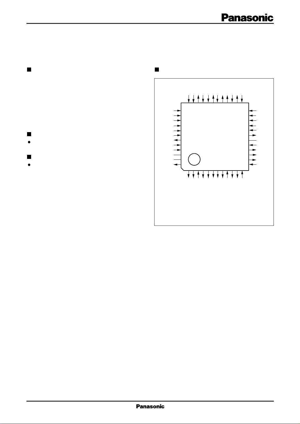
Pin Assignment Overview
The MN3111H is a vertical driver LSI for a two-dimensional interline CCD image sensor. It features a built-in
power supply circuit that, in conjunction with such
external components as four booster capacitors, six voltage stabilization capacitors, eight Schottky barrier diodes,
and two Zener diodes, produces stabilized +15.0V and
–10.0V power supplies from a +5.0V input and HD pulses.
Features
Single 5 volt power supply
Applications
Video cameras
ISUB
CH1
IV1
IV3
CH2
SENSE2
V
OUT–
V
IN –
GND
N.C.
N.C.
C4 –
EEVHH
V
OSUB
3635343332313029282726
37
38
39
40
41
42
43
44
45
46
47
48
1234567891011
VL2VL1OV1
V
M13
OV3
OV2
V
M24
OV4
V
25
24
23
22
21
20
19
18
17
16
15
14
13
12
H
V
DD
V
CC2
IV2
IV4
SENSE1
V
OUT+
N.C.
V
IN+
CAP3
CAP2
CAP1
TEST
EE
C2–
C3+
C3 –
GND
OV
(TOP VIEW)
QFH048-P-0707
C2+
C1+
C1–
DD
CC1
HD
C4+
V
OV
Page 2
MN3111H For Video Equipment
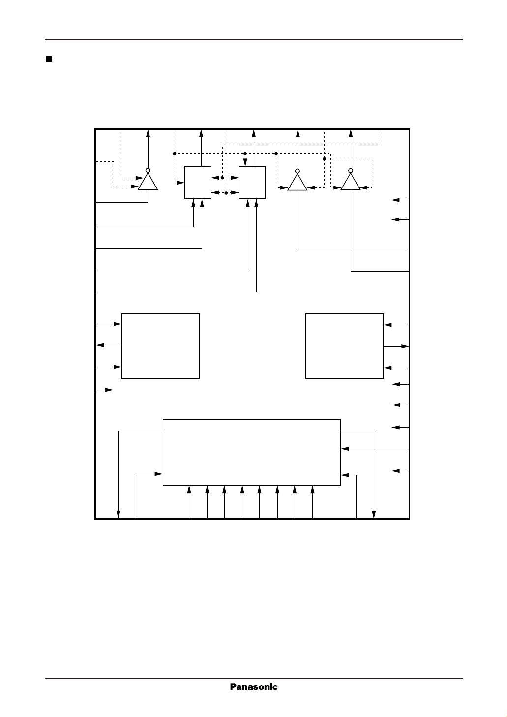
Block Diagram
VL2
V
ISUB
IV1
CH1
IV3
CH2
SENSE2
V
OUT–
V
IN –
GND
HH
V
34
35
OSUB31V
32
L1
OV129V
30
M13
OV3
28
OV2
M24
V
27
26
OV4
H
V
25
33
36
EE
Tristate
driver
37
39
38
40
Tristate
driver
24
V
DD
23
V
CC2
22
IV2
21
IV4
41
42
43
Negative voltage
monitor
Positive voltage
monitor
44
45
Negative and positive boosting voltage generator
20
19
17
16
15
14
12
13
SENSE1
V
OUT+
V
IN+
CAP3
CAP2
CAP1
HD
TEST
3
1
EE
GND
OV
8
C1–
7
C1+
4
6
5
2
48
10
C2–
C2+
C3 –
C3+
C4 –
C4+
9
11
DD
CC1
V
OV
Page 3
For Video Equipment MN3111H
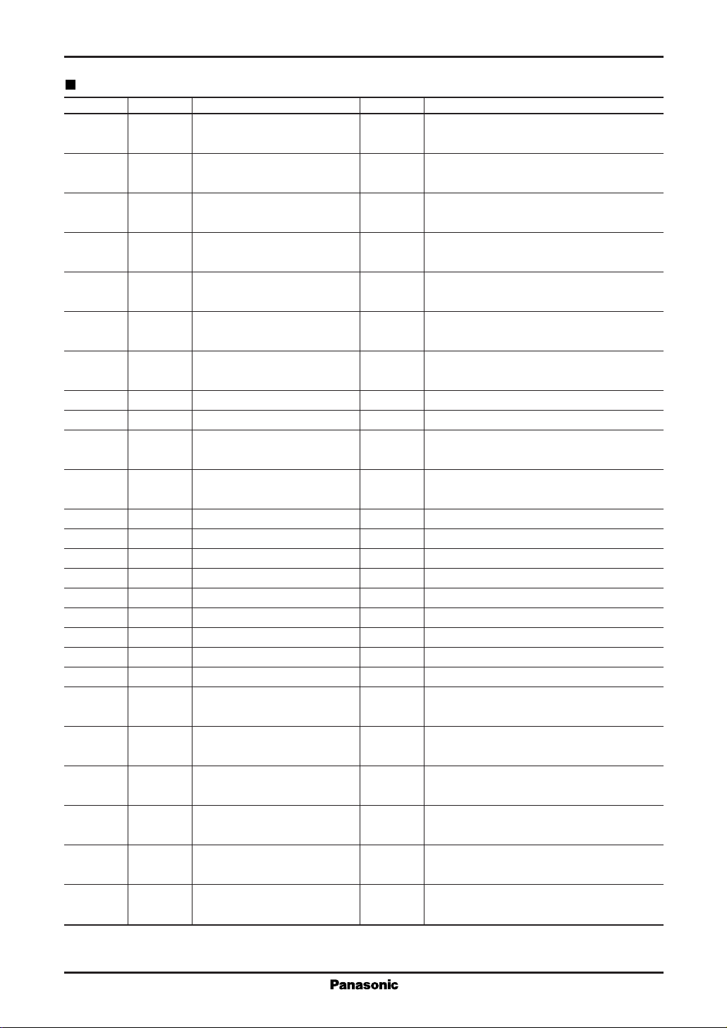
Pin Descriptions
Pin No. Symbol Pin Name I/O Function Description
9V
23 V
CC1
CC2
3 GND "L" level power supply I "L" level input for 5 volt circuits
45 for input block
25 V
35 V
30 V
27 V
32 V
33 V
24 V
36 V
17 V
44 V
H
HH
M13
M24
L1
L2
DD
EE
IN+
IN –
13 TEST Test input I Test pin (Keep this pin at "H" level.)
12 HD HD pulse input I HD pulse input pin
22 IV2 Transfer pulse input I Charge transfer pulse input pin
21 IV4 Transfer pulse input I Charge transfer pulse input pin
39 IV1 Transfer pulse input I Charge transfer pulse input pin
40 IV3 Transfer pulse input I Charge transfer pulse input pin
38 CH1 Charge pulse input I Charge readout pulse input pin
41 CH2 Charge pulse input I Charge readout pulse input pin
37 ISUB SUB pulse input I Unwanted charge rejection pulse input pin
20 SENSE1 Positive voltage monitor I Positive voltage monitor control sensing
42 SENSE2 Negative voltage monitor I Negative voltage monitor control sensing
7 C1+ C1 connection O Booster block voltage charging capacitor
8 C1– connection pins
6 C2+ C2 connection O Booster block voltage charging capacitor
4 C2– connection pins
2 C3+ C3 connection O Booster block voltage charging capacitor
5 C3 – connection pins
10 C4+ C4 connection O Booster block voltage charging capacitor
48 C4 – connection pins
"H" level power supply I "H" level input for 5 volt circuits
for input block
"H" level power supply I "H" level input for high-voltage circuits
for vertical driver
"H" level power supply I "H" level input for high-voltage circuits
for SUB driver
"M" level power supply I "M" level input for high-voltage circuits
for vertical driver
"L" level power supply I "L" level input for high-voltage circuits
for vertical driver
"L" level power supply I "L" level input for high-voltage circuits
for SUB driver
Driver power supply 1 I "H" level for high-voltage circuits
Driver power supply 2 I "L" level for high-voltage circuits
Voltage input for positive I Voltage input pin for positive voltage
voltage monitor monitor
Voltage input for negative I Voltage input pin for negative voltage
voltage monitor monitor
sensing input pin (Leave this pin open.)
sensing input pin (Leave this pin open.)
Page 4
MN3111H For Video Equipment
Pin Descriptions (continued)
Pin No. Symbol Pin Name I/O Function Description
11 OV
1OV
19 V
43 V
DD
EE
OUT+
OUT-
26 OV4 Binary transfer pulse O Binary (V
28 OV2 Binary transfer pulse O Binary (V
29 OV3 Tristate transfer pulse O Tristate (V
31 OV1 Tristate transfer pulse O Tristate (V
34 OSUB SUB pulse output O Unwanted charge (V
14 CAP1 Stabilizing capacitor O Pins for connecting capacitors for internal
15 CAP2 connection voltage stabilization circuits
16 CAP3
18 N.C. No connection —
46
47
Booster block positive O Booster block positive voltage
voltage output output pin
Booster block negative O Booster block negative voltage
voltage output output pin
Positive regulated voltage O Positive voltage monitor output pin
output (Leave this pin open.)
Negative regulated voltage O Negative voltage monitor output pin
output (Leave this pin open.)
, VL1) transfer pulse
M24
output output pin
, VL1) transfer pulse
M24
output output pin
, V
H
, VL1) transfer pulse
M13
output output pin
, V
H
, VL1) transfer pulse
M13
output output pin
, VL2) rejection
HH
pulse input pin
Page 5

For Video Equipment MN3111H
Functional Description
Binary transfer pulses (vertical driver block)
IV2 OV2
IV4 OV4
HL
LM
Tristate transfer pulses (vertical driver block)
CH1 IV1 OV1
CH2 IV3 OV3
H
L
1
*
IV1, IV2, IV3, IV4, CH1, CH2
H: V
CC
L: GND
OV1, OV2, OV3, OV4
H: V
H
M: V
, or V
L: V
M13
L1
M24
HL
LM
HL
LH
Unwanted charge rejection pulses (SUB driver block)
ISUB OSUB
HL
LH
1
*
ISUB
H: V
CC
L: GND
OSUB
H: V
HH
L: V
L2
Page 6

MN3111H For Video Equipment
Electrical Characteristics
(1) DC characteristics
VHH=VH=15.0V, V
V
CC1=VCC2
M13=VM24
=5.0V (=VCC), VL1=–7.0V, VL2=–10.0V, Ta=+25˚C
Parameter Symbol Test conditions min typ max Unit
Quiescent supply current I
Operating supply current I
Power supply output pins OV
Positive voltage stabilization V
circuit output voltage
Negative voltage stabilization V
circuit output voltage
Input pins IV1, IV2, IV3, IV4, CH1, CH2, ISUB, HD
"H" level voltage V
"L" level voltage V
Input leak current I
Output pins 1 (Binary output) OV2, OV4
Output voltage "M" level V
Output voltage "L" level V
Output on resistance "M" level R
Output on resistance "L" level R
Output pins 2 (Tristate output) OV1, OV3
Output voltage "H" level V
Output voltage "M" level V
Output voltage "L" level V
Output on resistance "H" level R
Output on resistance "M" level R
Output on resistance "L" level R
Output pin 3 (SUB output) OSUB
Output voltage "H" level V
Output voltage "L" level V
Output on resistance "H" level R
Output on resistance "L" level R
=1.0V, GND=0.0V,
DDST
DDDYNVI
DD
REG+
REG-
IH
IL
LI
OM1
OL1
ONM1IOM1
ONL1IOL1
OH2
OM2
OL2
ONH2IOH2
ONM2IOM2
ONL2IOL2
OHH3
OL3
ONHH3IONHH3
ONL3IONL3
VI=GND, V
=GND, V
, OV
EE
VI=GND, V
VI=GND, V
CC
CC
, IO=7mA 14.5 15.0 15.5 V
CC
, IO=–2mA –10.5 –10.0 –9.5 V
CC
3.5 V
4 mA
11 mA
V
CC
GND 1.5 V
VI=0 to 5V ±1 µA
VI=GND, V
VI=GND, V
, I
CC
CC
=–1mA 0.9 V
OM1
, I
=1mA V
OL1
M24
L1
–6.9 V
V
=–50mA 40 Ω
=50mA 40 Ω
VI=GND, V
VI=GND, V
VI=GND, V
, I
= –1mA 14.9 V
CC
OH2
, I
CC
CC
=–1mA 0.9 V
OM2
, I
=1mA V
OL2
V
H
M13
L1
–6.9 V
V
=–50mA 50 Ω
=±50mA 40 Ω
=50mA 40 Ω
VI=GND, V
VI=GND, V
, I
CC
OHH3
, I
=1mA V
CC
OL3
=–1mA 14.9 V
L2
HH
–9.9 V
V
=–50mA 50 Ω
=50mA 40 Ω
Page 7

For Video Equipment MN3111H
(2) AC characteristics
VHH=VH=15.0V, V
V
CC1=VCC2
M13=VM24
=5.0V (=VCC), VL1=–7.0V, VL2=–10.0V, Ta=+25˚C
Parameter Symbol Test conditions min typ max Unit
Output pins 1 (Binary output) OV2, OV4
Transmission delay t
Rise time t
Fall time t
Output pins 2 (Tristate output) OV1, OV3
Transmission delay t
Transmission delay t
Rise time t
Fall time t
Rise time t
Fall time t
Output pin 3 (SUB output) OSUB
Transmission delay t
Rise time t
Fall time t
=1.0V, GND=0.0V,
PLM
t
PML
TLM
TML
PLM
t
PML
PMH
t
PHM
TLM
TML
TMH
THM
PLHH
t
PHHL
TLHH
THHL
No load
From "L" level to "M" level
No load
From "L" level to "M" level
No load
From "M" level to "H" level
No load
From "L" level to "H" level
100 200 ns
200 300 ns
100 200 ns
200 400 ns
200 300 ns
200 300 ns
100 200 ns
200 300 ns
Page 8

MN3111H For Video Equipment
Timing Chart
1. Binary transfer pulses
63.5µs
2µs
IV2
OV2
2. Binary transfer pulses
IV4
OV4
3. Tristate transfer pulses
IV1
CH1
3µs
63.5µs254µs
H
L
M
L
H
L
M
L
H
L
H
L
H
OV1
4. Tristate transfer pulses
IV3
CH2
OV3
5. SUB pulses
ISUB
OSUB
M
L
H
L
H
L
H
M
L
H
L
H
L
Page 9

For Video Equipment MN3111H
Application Circuit Example
1
*
D11
D12
>
–10.0V
<
37
38
39
40
from clock generator
+
C13
D10
41
42
43
44
45
46
47
48
to CCD’s
>
–7.9V
<
D13
+
C19
36
EE
V
ISUB
CH1
IV1
IV3
CH2
SENSE2
V
OUT–
V
IN –
GND
NC
NC
C4 –
PT pin
D14
C20
35
HH
V
C18
R7
+
34
OSUB
+
C17
>
–7V
<
33
32
L2VL1
V
MN3111H
Diode with V
Schottky barrier diode
Zener diode
to CCD’s
øV pin
31
30
29
M13
OV1
OV3
V
28
OV2
=0.7V
F
27
M24
V
26
25
H
V
OV4
DD
V
CC2
IV2
IV4
SENSE1
V
OUT+
NC
V
IN+
CAP3
CAP2
CAP1
TEST
R6
to CCD’s source
follower power
supply for OD,
RD, and IS pins
D15
R4
R3
C16
R5
C15
+
+
C14
1
*
>
+15.0V
<
24V
23
22
21
from clock
20
19
+
C12
generator
18
17
D9
16
15
C11
14
13
C10
C7
EE
OV
1
R1
D7
D2
C1–
8
C5
+
V
9
CC1
D6
C4+
10
+
OVDDHD
11
12
C8
C3+
GND
C2–
C3 –
C2+
C1+
2
3
4
5
6
7
D4
D3
C6
+
D1
C1
D5
+
+
C3
C2
+
C4
+
R2
D8
The booster circuit's electrolytic capacitors must have little impedance fluctuation at low temperatures.
Note *1: These diodes must have a V
of 0.7 V. All other diodes, except the Zener diodes, must be
F
Schottky barrier diodes (MA723).
C9
5 volt input
Page 10

MN3111H For Video Equipment
Package Dimensions (Unit: mm)
QFH048-P-0707
9.0
±0.2
7.0
±0.2
36 25
37
48
(0.75)
24
(0.75)
±0.2
±0.2
7.0
9.0
13
1
0.5
0.2
12
±0.1
(1.0)
0.05
-
+0.10
2.9 max.
0.15
0.5
±0.2
0 to 10°
0.1
SEATING PLANE
±0.2
2.5
±0.1
0.1
Page 11

For Video Equipment MN3111H
Usage Notes
External components
1. This product requires eight Schottky barrier diodes and two Zener diodes.
We recommend the following components.
Schottky barrier diodes: MA723 or equivalents
Zener diodes: MA1150-M, MA8150-M (for positive regulated voltage) or equivalents
MA1100-M, MA8100-M (for negative regulated voltage) or equivalents
Ta=25˚C
Component Model number Typical characteristics Notes
Schottky barrier diodes MA723 I
MA1150-M
Zener diodes
MA8150-M regulated voltage
MA1100-M
MA8100-M regulated voltage
The MN3111H will not operate properly if the components do not satisfy the above specifications.
=200mA, VF ≤ 0.55V
F
=5mA, 14.6V ≤ VZ ≤ 15.35V
I
Z
=5mA, 9.75V ≤ VZ ≤ 10.25V
I
Z
for positive
for negative
2. Always use the specified components for peripheral circuits so as to ensure that OVEE and VL do not reverse
potentials when the power is turned off.
Normal operation
GND
V
L1/VL2
OV
EE
As the above sketch illustrates, allowing OV
OFF
GND
V
L1/VL2
OV
to exceed VL1 and VL2 by more than 0.7 V produces the risk
EE
Faulty operation
0.7V or higher
Reversal
EE
OFF
of applying a forward bias to the PN junction, turning on the parasitic transistor, and generating an
overcurrent that produces latch-up.
If this phenomenon arises, increase the size of capacitor C7 or decrease the size of capacitor C13 to increase
the OV
time constant.
EE
(See the sample application circuit for the locations of C7 and C13.)
 Loading...