

Page 1
MICROWAVE CORPORATION
0.5 dB LSB GaAs IC 5 - BIT DIGITAL ATTENUATOR 0.7 - 4 GHz
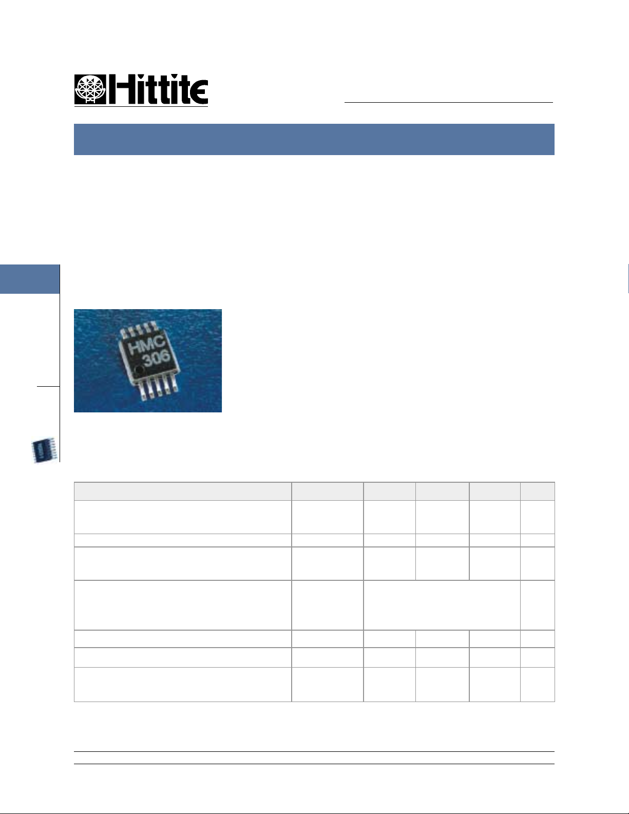
HMC306MS10
2
ATTENUATORS
SMT
FEBRUARY 2001
Features
0.5 dB LSB STEPS to 15.5 dB
General Description
The HMC306MS10 is a broadband 5-bit positive control GaAs IC digital attenuator in a 10
SINGLE POSITIVE CONTROL PER BIT
+/- 0.25 dB TYPICAL BIT ERROR
MINIATURE MSOP-10 PACKAGE: 14.8 mm²
lead MSOP surface mount plastic package.
Covering 0.7 to 4 GHz, the insertion loss is
typically less than 1.5 to 2.3 dB. The attenuator bit values are 0.5 (LSB), 1, 2, 4 and 8 for a
total attenuation of 15.5 dB. Attenuation accuracy is excellent at ± 0.25 dB typical with an
IIP3 of up to +52 dBm. Five bit control voltage
inputs, toggled between 0 and +3 to +5V, are
used to select each attenuation state at less
than 50 uA each. A single Vdd bias of +3 to
+5V applied through an external 5KΩ resistor
is required. The HMC306MS10 is ideal for
cellular, PCS, ISM, MMDS, and WLL applications while occupying less than 14.8 mm².
Guaranteed Performance
With Vdd =+3V to +5V & Vctl = 0/Vdd (Unless Otherwise Stated), -40 to +85 deg C
V00.0600
Parameter Frequency Min. Typ. Max. Units
0.7 - 1.4 GHz
Insertion Loss
Attenuation Range 15.5 dB
ReturnLoss (RF1 & RF2,All Atten.States)
Attenuation Accuracy:(Referenced to Insertion Loss)
All Attenuation States
All Attenuation States
All Attenuation States
0.5 - 13.5 dB States
14 - 15.5 dB States
Input Power for 0.1 dB Compression Vdd= 5V
Input Third Order Intercept Point
(Tw o-Tone Input Power = 0dBm Each)
Switching Characteristics
tRISE, tFALL (10/90%RF)
tON/tOFF (50% CTL to 10/90% RF)
12 Elizabeth Drive, Chelmsford, MA 01824 Phone: 978-250-3343 Fax: 978-250-3373 Web Site: www.hittite.com
Vdd= 3V
Vdd= 5V
Vdd= 3V
1.4 - 2.3 GHz
2.3 - 2.7 GHz
2.7 - 4.0 GHz
0.7 - 1.4 GHz
1.4 - 2.3 GHz
2.3 - 2.7 GHz
2.7 - 4.0 GHz
0.7 - 1.4 GHz
1.4 - 2.3 GHz
2.3 - 2.7 GHz
2.7 - 4.0 GHz
2.7 - 4.0 GHz
0.7-4.0 GHz 25
0.7-4.0 GHz 52
0.7 - 4.0 GHz
15
14
13
10
± 0.30 + 3% of A tten.S etting Max
± 0.25 + 2% of A tten.S etting Max
± 0.25 + 3% of A tten.S etting Max
± 0.30 + 3% of A tten.S etting Max
± 0.35 + 5% of Atten.Setting Max
1.3
1.5
1.8
2.3
21
18
16
13
23
48
560
600
1.6
2.0
2.5
2.7
dB
dB
dB
dB
dB
dB
dB
dB
dB
dB
dB
dB
dB
dBm
dBm
dBm
dBm
ns
ns
2 - 74
Page 2
MICROWAVE CORPORATION
0.5 dB LSB GaAs IC 5 - BIT DIGITAL ATTENUATOR 0.7- 4 GHz
HMC306MS10
V00.0600
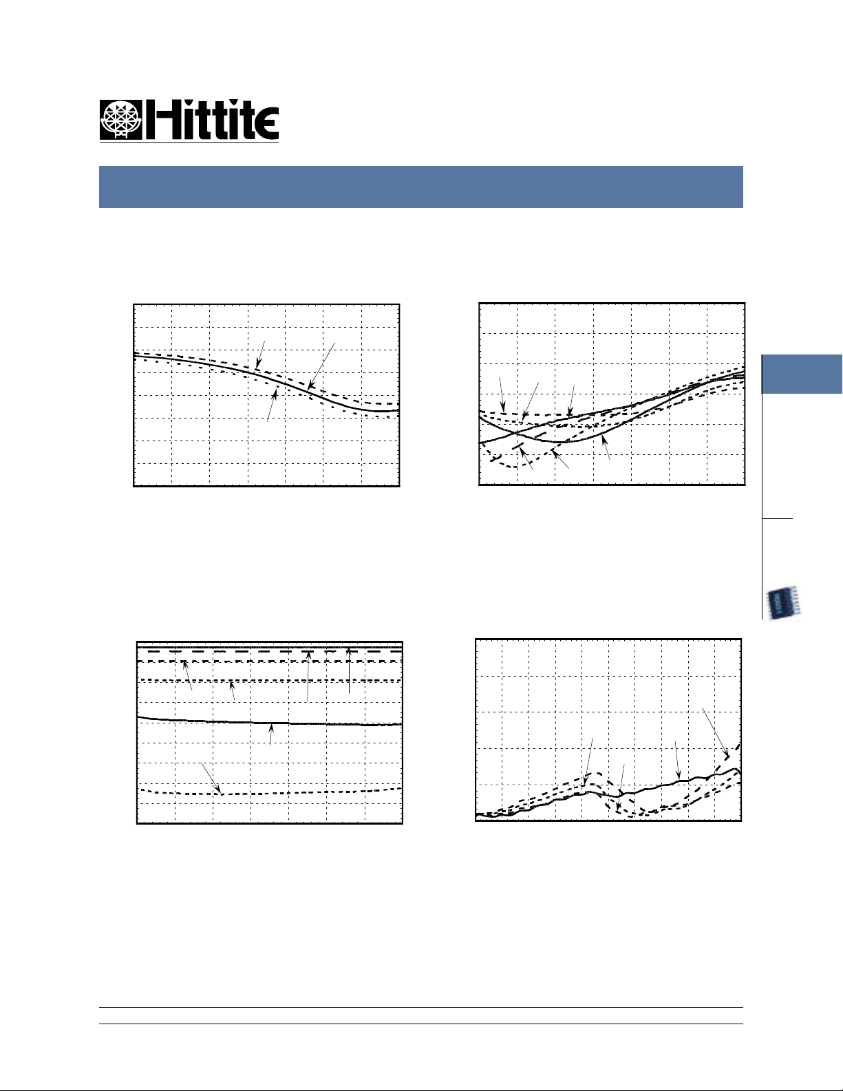
Insertion Loss
0
-0.5
-1
-1.5
-2
-2.5
INSERTION LOSS (dB)
-3
-3.5
-4
0.5 1 1.5 2 2.5 3 3.5 4
-40 C
+85 C
FREQUENCY (GHz)
+25 C
Normalized Attenuation
(Only Major States are Shown)
0
-2
-4
-6
-8
-10
-12
-14
NORMALIZED ATTENUATION (dB)
-16
-18
0.5 1 1.5 2 2.5 3 3.5 4
2dB
4dB
15.5 dB 8 dB
FREQUENCY (GHz)
1dB
0.5 dB
FEBRUARY 2001
Return Loss RF1, RF2
Only Major States are Shown)
(
0
-5
-10
2dB
-15
-20
RETURN LOSS (dB)
-25
-30
0.5 1 1.5 2 2.5 3 3.5 4
0.5 dB
4dB
15.5 dB
1dB
FREQUENCY (GHz)
8dB
Absolute Bit Error vs Attenuation State
1.5
1.2
0.9
2.4 GHz
0.6
BIT ERROR (dB)
0.3
0
0.5 2 3.5 5 6.5 8 9.5 11 12.5 14 15.5
ATTENUATION STATE (dB)
1.9 GHz
3.5 GHz
0.9 GHz
2
ATTENUATORS
SMT
Note: All Data Typical Over Voltage (+3V to +5V) & Temperature (-40 to +85 deg.C).
S-Parameter data is available On-Line at www.hittite.com
12 Elizabeth Drive, Chelmsford, MA 01824 Phone: 978-250-3343 Fax: 978-250-3373 Web Site: www.hittite.com
2 - 75
Page 3

MICROWAVE CORPORATION
0.5 dB LSB GaAs IC 5 - BIT DIGITAL ATTENUATOR 0.7- 4 GHz
HMC306MS10
2
ATTENUATORS
SMT
FEBRUARY 2001
Absolute Bit Error vs Frequency
Only Major States are Shown)
(
1.5
1.2
8dB
0.9
0.6
BIT ERROR (dB)
0.3
0
0.5 1 1.5 2 2.5 3 3.5 4
0.5, 1, 2 dB
15.5 dB
FREQUENCY (GHz)
4dB
Functional Diagram/
Application Circuit
PIN NUMBER
V5
1
0.5 dB
10
100 pF
C1
Relative Phase vs Frequency
Only Major States are Shown)
(
60
40
20
0
RELATIVE PHASE (deg.)
-20
-40
0.5 1 1.5 2 2.5 3 3.5 4
FREQUENCY (GHz)
T ruth Table
Control Voltage Input
V1
8dBV24dBV32dBV41dBV50.5dB
High High High High High
High High High High Low 0.5 dB
RF1
High High High Low High 1dB
15.5 dB
0.5, 1 dB
V00.0600
8dB
4dB
2dB
Attenuation
State
RF1 - RF2
Reference
I.L.
V4
2
V3
3
V2
4
V1
5
DC Blocking capacitors C1 & C2 are required on RF1 & RF2. Choose
C1 = C2 = 100 ~ 300 pF to allow lowest customer specific frequency to
pass with minimal loss. R1 = 5KΩ is required to supply voltage to the
circuit through either PIN 6 or PIN 10.
1 dB
2 dB
4 dB
8 dB
9
8
7
100 pF
6
R1
5 k W
Vdd
RF2
C2
High High Low High High 2dB
High Low High High High 4dB
Low High High High High 8dB
Low Low Low Low Low
Anycombination of above states will p rovide an
attenuation approximately equal to the sum of the bits
selected.
15.5 dB
Max Atten.
Control & Bias Voltages
State Bias Condition
Low 0 to +0.2V@ 20uA Max
High Vdd ± 0.2V @ 100 uA Max
Note: Vdd = +3V to 5V ± 0.2 V
12 Elizabeth Drive, Chelmsford, MA 01824 Phone: 978-250-3343 Fax: 978-250-3373 Web Site: www.hittite.com
2 - 76
Page 4

MICROWAVE CORPORATION
0.5 dB LSB GaAs IC 5 - BIT DIGITAL ATTENUATOR 0.7- 4 GHz
HMC306MS10
V00.0600
Absolute Maximum Ratings
Control Voltage (V1 - V5) Vdd + 0.5 Vdc
Bias Voltage (Vdd) +8.0 Vdc
Storage Temperature -6 5 to +150 deg C
Operating Temperature - 40 to +85 deg C
RF Input Power (0.7 - 4 GHz) +28 dBm
Outline
FEBRUARY 2001
2
ATTENUATORS
SMT
1. MATERIAL:
A) PACKAGE BODY - LOW STRESS INJECTION-MOLDED PLASTIC.
B) LEADFRAME MATERIAL: COPPER ALLOY
2 . PLATING : LEAD - TIN SOLDER PLATE
3. DIMENSIONS ARE IN INCHES (MILLIMETERS).
UNLESS OTHERWISE SPECIFIED ALL TOL. ARE ±0.005(±0.13).
12 Elizabeth Drive, Chelmsford, MA 01824 Phone: 978-250-3343 Fax: 978-250-3373 Web Site: www.hittite.com
4. DIMENSION DOES NOT INCLUDE MOLDFLASH OF 0.15 MM PER SIDE
5. DIMENSION DOES NOT INCLUDE MOLDFLASH OF 0.25 MM PER SIDE
2 - 77
Page 5

MICROWAVE CORPORATION
0.5 dB LSB GaAs IC 5 - BIT DIGITAL ATTENUATOR 0.7 - 4 GHz
HMC306MS10
2
ATTENUATORS
SMT
FEBRUARY 2001
Evaluation Circuit Board
V00.0600
* R2 - R6 = 100 Ω .
These resistors are optional and
may be used to enhance
decoupling of the RF path from
the control inputs.
The circuit board used in the final application should use RF circuit design techniques. Signal lines should have
50 ohm impedance while the package ground leads should be connected directly to the ground plane similar to
that shown above. A sufficient number of VIA holes should be used to connect the top and bottom ground planes.
The evaluation circuit board as shown is available from Hittite upon request.
Evaluation Circuit Board Layout Design Details
Item Description
J1 - J2 PC Mount SMA Connector
J3 - J8 DC Pin
R1 5k Ω Resistor, 0402 Pkg.
R2 - R6 100 Ω Resistor, 0402 Pkg.
C1, C2 0402 Chip Capacitor, Select Value for
Lowest Frequency
U1 HMC306MS10 Digital Attenuator
PCB* 103391 Evaluation PCB 1.5" x 1.5"
*Circuit Board Material: Rogers 4350
12 Elizabeth Drive, Chelmsford, MA 01824 Phone: 978-250-3343 Fax: 978-250-3373 Web Site: www.hittite.com
2 - 78
Page 6

MICROWAVE CORPORATION
0.5 dB LSB GaAs IC 5 - BIT DIGITAL ATTENUATOR 0.7 - 4 GHz
HMC306MS10
V00.0600
NOTES:
FEBRUARY 2001
2
ATTENUATORS
SMT
12 Elizabeth Drive, Chelmsford, MA 01824 Phone: 978-250-3343 Fax: 978-250-3373 Web Site: www.hittite.com
2 - 79
 Loading...