

Page 1
查询HMC240供应商
7
MICROWAVE CORPORATION
Typical Applications
The HMC240 is ideal for:
• Telecom Infrastructure
• Microwave Radio & VSAT
• Military & Space
• Test Instrumentation
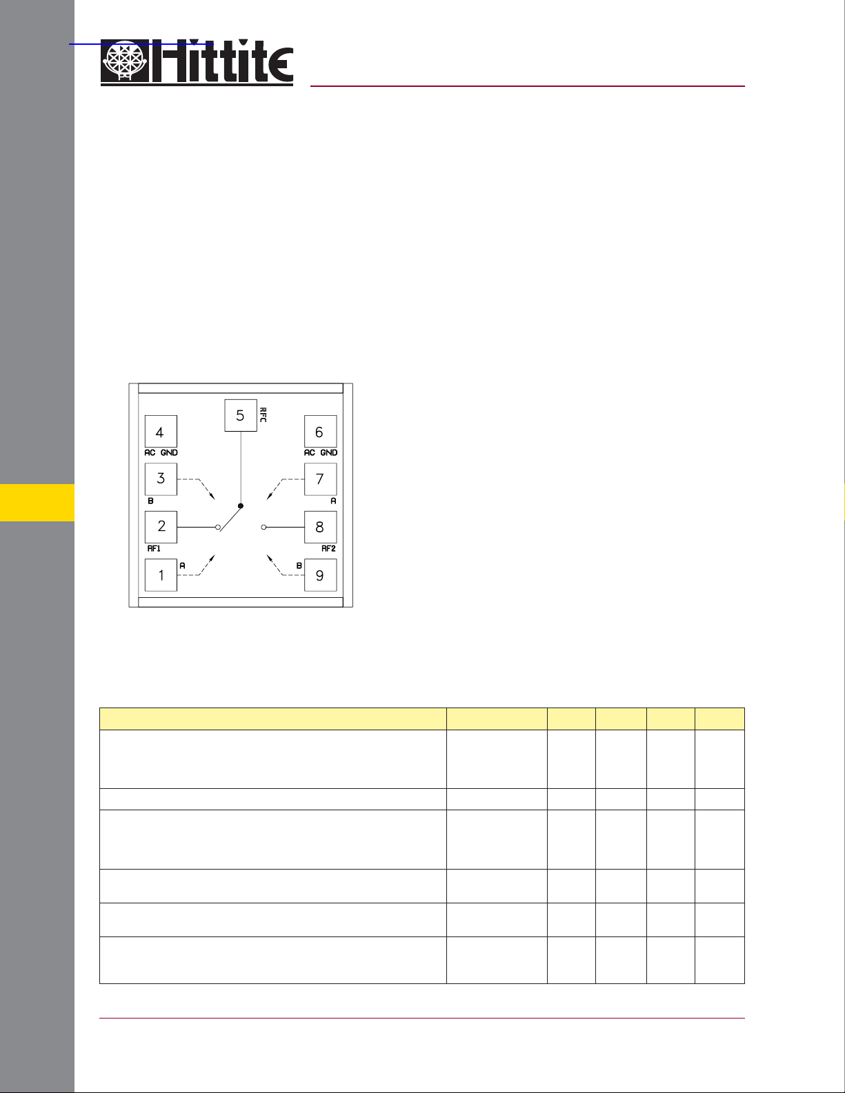
Functional Diagram
v00.0403
HMC240
GaAs MMIC SPDT SWITCH
DC - 4.0 GHz
Features
Broadband Performance: DC - 4.0 GHz
Low Insertion Loss: 0.5 dB @ 2.0 GHz
High IIP3: +48 dBm
Small Size: 0.70 mm x 0.70 mm x 0.13 mm
General Description
The HMC240 is a low cost GaAs MESFET SPDT
switch chip. Cov ering DC to 4.0 GHz, this s witch
offers high isolation and low insertion loss. RF1
and RF2 are refl ective shorts when “off”. The
switch can operate using either two negativ e control logic inputs of -5/0V or two positive control
voltage logic inputs of 0/+5V. All data is tested
with the chip in a 50 Ohm test fi xture connected
via 0.025 mm (1 mil) diameter wire bonds of 0.31
mm (12 mils) length.
Pads 3 & 7 are alternate A & B Control Inputs.
Electrical Specifi cations, T
With 0/-5V Control or +5/0V Control, 50 Ohm System
Parameter Frequency Min. Typ. Max. Units
Insertion Loss
SWITCHES - CHIP
Isolation DC - 4.0 GHz 24 28 dB
Return Loss “On State”
Input Power for 1 dB Compression
Input Third Order Intercept
(Two-Tone Input Power= +7 dBm Each Tone)
Switching Characteristics
tRISE, tFALL (10/90% RF)
tON, tOFF (50% CTL to 10/90% RF)
= +25° C,
A
DC - 1.0 GHz
DC - 2.0 GHz
DC - 3.0 GHz
DC - 4.0 GHz
DC - 1.0 GHz
DC - 2.0 GHz
DC - 3.0 GHz
DC - 4.0 GHz
0.5 - 1.0 GHz
0.5 - 4.0 GHz
0.5 - 1.0 GHz
0.5 - 4.0 GHz
DC - 4.0 GHz
0.4
0.5
0.6
0.9
22
16
14
11
25
23
43
40
30
29
48
45
3
10
0.7
0.8
0.9
1.4
dB
dB
dB
dB
dB
dB
dB
dB
dBm
dBm
dBm
dBm
ns
ns
7 - 8
For price, delivery, and to place orders, please contact Hittite Microwave Corporation:
12 Elizabeth Drive, Chelmsford, MA 01824 Phone: 978-250-3343 Fax: 978-250-3373
Order Online at www.hittite.com
Page 2

v00.0403
HMC240
MICROWAVE CORPORATION
GaAs MMIC SPDT SWITCH
DC - 4.0 GHz
GaAs MMIC SUB-HARMONICALLY PUMPED MIXER 17 - 25 GHz
Insertion Loss vs. Temperature Isolation
0
-0.5
-1
-1.5
-2
INSERTION LOSS (dB)
-2.5
-3
0 0.5 1 1.5 2 2.5 3 3.5 4
+25 C
+85 C
-55 C
FREQUENCY (GHz)
Return Loss 0.1 and 1 dB Input Compression Point
0
-5
-10
-15
-20
RETURN LOSS (dB)
-25
-30
0 0.5 1 1.5 2 2.5 3 3.5 4
RFC
RF1, RF2, ON
FREQUENCY (GHz)
0
-5
-10
-15
-20
-25
-30
ISOLATION (dB)
-35
-40
-45
-50
0 0.5 1 1.5 2 2.5 3 3.5 4
32
31
30
29
28
27
26
25
INPUT P1dB (dBm)
24
23
22
0.5 1 1.5 2 2.5 3 3.5 4
RF1
RF2
FREQUENCY (GHz)
1.0 dB Compression Point
0.1 dB Compression Point
FREQUENCY (GHz)
7
Input Third Order Intercept Point
60
55
50
45
40
INPUT IP3 (dBm)
35
30
0.5 1 1.5 2 2.5 3 3.5 4
For price, delivery, and to place orders, please contact Hittite Microwave Corporation:
12 Elizabeth Drive, Chelmsford, MA 01824 Phone: 978-250-3343 Fax: 978-250-3373
Order Online at www.hittite.com
+25 C
+85 C
-40 C
FREQUENCY (GHz)
SWITCHES - CHIP
7 - 9
Page 3
MICROWAVE CORPORATION
v00.0403
Absolute Maximum Ratings
HMC240
GaAs MMIC SPDT SWITCH
DC - 4.0 GHz
7
RF Input Power
V
= 0/+5 (-5)V
ctrl
Control Voltage Range (A & B= 0/+5V) -0.2 to +10 Vdc
Control Voltage Range (A & B= -5/0V) -10 to +0.2 Vdc
Storage Temperature -65 to +150 deg C
Operating Temperature -55 to +85 deg C
<
0.5 GHz
0.5 - 4 GHz
+27 dBm
+34 dBm
Positive Control Voltage
State Bias Condition
Low 0 Vdc @ 10 uA
High +3 Vdc @ 10 uA to +8 Vdc @ 70 uA
Control input voltage tolerences are ±0.2 Vdc.
T ruth T able: Positive Control Voltage
Control Input Control Current Signal Path State
A
(Vdc)B(Vdc)
0 +5 -50 50 ON OFF
+5 0 50 -50 OFF ON
Ia
(uA)
Ib
(uA)
RFC to
RF1
RFC to
RF2
Negative Control Voltage
State Bias Condition
Low -3 Vdc @ 10 uA to -8 Vdc @ 70 uA
High 0 Vdc @ 10 uA
Control input voltage tolerences are ±0.2 Vdc.
T ruth T able: Negative Control Voltage
Control Input Control Current Signal Path State
A
(Vdc)B(Vdc)
-5 0 -50 50 ON OFF
0 -5 50 -50 OFF ON
Ia
(uA)
Ib
(uA)
RFC to
RF1
RFC to
RF2
Note:
This part can be controlled with either positive or negative voltages per the above table. DC blocks are required at ports RFC, RF1
and RF2 if positive control voltage is used.
SWITCHES - CHIP
For price, delivery, and to place orders, please contact Hittite Microwave Corporation:
7 - 10
12 Elizabeth Drive, Chelmsford, MA 01824 Phone: 978-250-3343 Fax: 978-250-3373
Order Online at www.hittite.com
Page 4
MICROWAVE CORPORATION
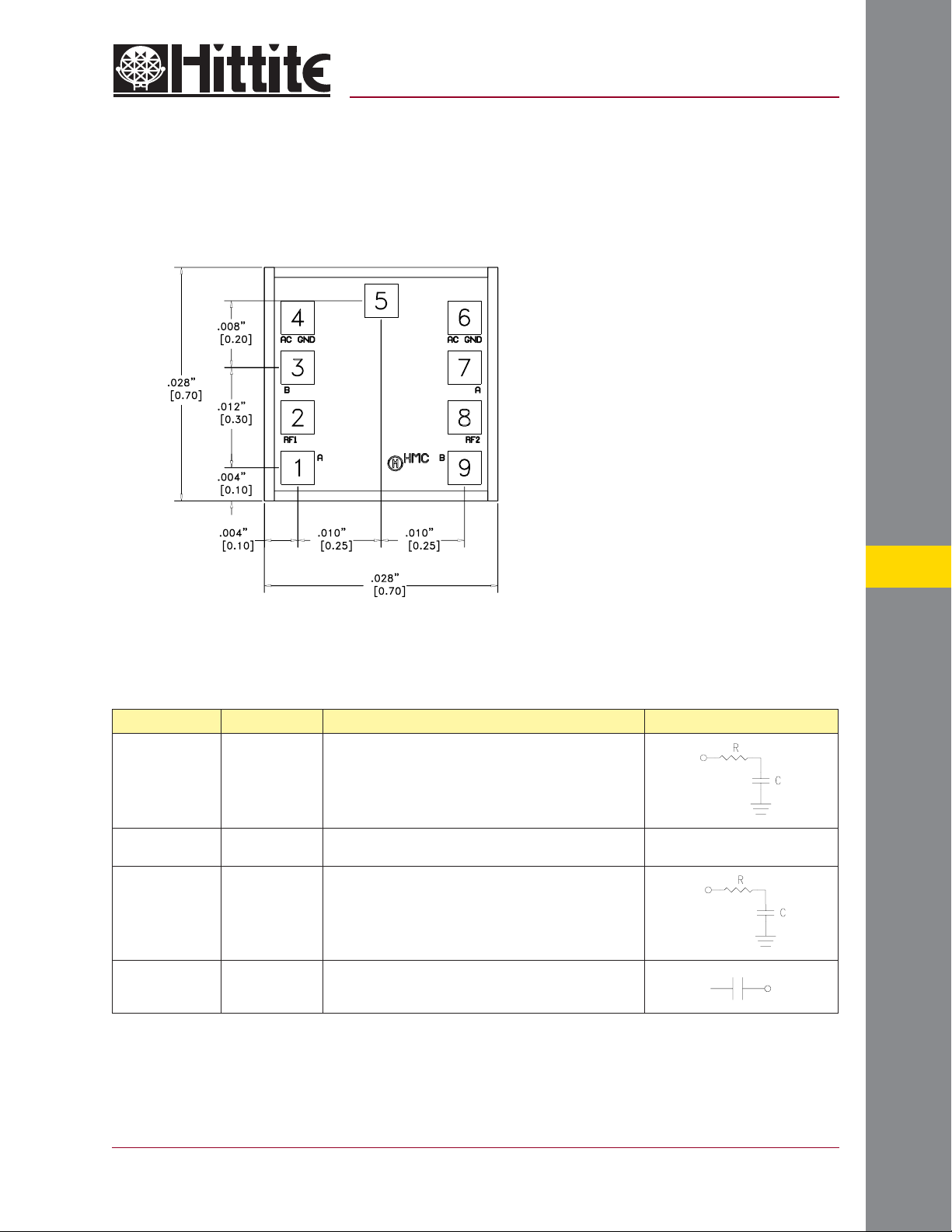
Outline Drawing
v00.0403
HMC240
GaAs MMIC SPDT SWITCH
DC - 4.0 GHz
NOTES:
1. DIMENSIONS IN INCHES [MILLIMETERS].
2. DIE THICKNESS IS 0.005”.
3. TYPICAL BOND PAD IS 0.004” SQUARE.
4. TYPICAL BOND PAD SPACING IS 0.006” CENTER TO CENTER.
5. BOND PAD METALLIZATION: GOLD.
6. PADS 4 AND 6 MUST BE CONNECTED TO RF/DC GROUND.
Pad Descriptions
Pad Number Function Description Interface Schematic
1, 7 A, A (alt.)
2, 5, 8 RF1, RFC, RF2
3, 9 B, B (alt.)
4, 6 AC GND Must be connected to RF/DC ground.
See truth table and control voltage table.
Connect either pad 1 or pad 7 to control logic input.
These pads are DC coupled and matched to 50 Ohms.
Blocking capacitors are required.
See truth table and control voltage table.
Connect either pad 3 or pad 9 to control logic input.
7
SWITCHES - CHIP
For price, delivery, and to place orders, please contact Hittite Microwave Corporation:
12 Elizabeth Drive, Chelmsford, MA 01824 Phone: 978-250-3343 Fax: 978-250-3373
Order Online at www.hittite.com
7 - 11
Page 5
MICROWAVE CORPORATION
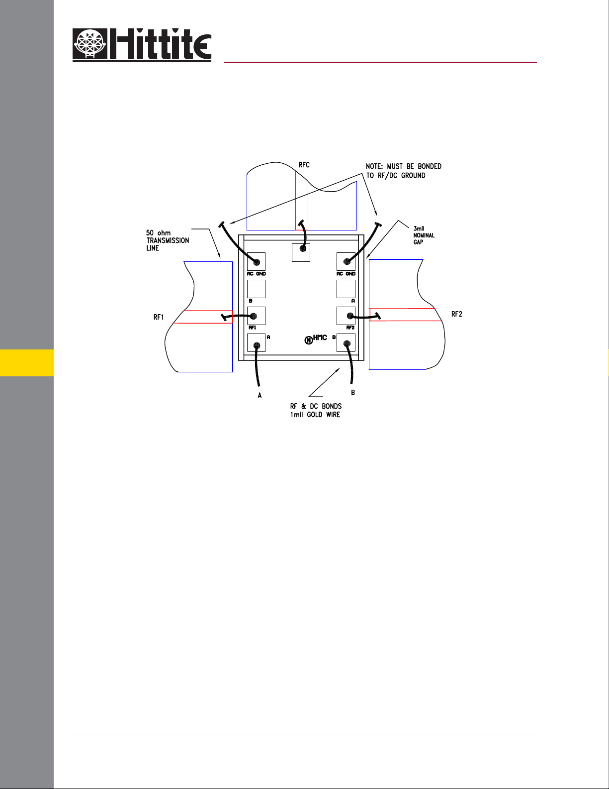
Assembly Diagram
v00.0403
HMC240
GaAs MMIC SPDT SWITCH
DC - 4.0 GHz
7
Handling Precautions
Follow these precautions to avoid permanent damage.
Cleanliness: Handle the chips in a clean environment. DO NOT attempt to clean the chip using liquid cleaning systems.
Static Sensitivity: Follow ESD precautions to protect against > ± 250V ESD strikes.
Transients: Suppress instr ument and bias supply transients while bias is applied. Use shielded signal and bias cables to minimize
inductive pick-up.
General Handling: Handle the chip along the edges with a vacuum collet or with a sharp pair of bent tweezers. The surface of the
chip has fragile air bridges and should not be touched with vacuum collet, tweezers, or fi ngers.
SWITCHES - CHIP
Mounting
The chip is back-metallized and can be die mounted with electrically conductive epoxy. The mounting surface should be clean and
fl at.
Epoxy Die Attach: Apply a minimum amount of epoxy to the mounting surface so that a thin epoxy fi llet is obser ved around the
perimeter of the chip once it is placed into position. Cure epoxy per the manufacturer’s schedule.
Wire Bonding
Ball or wedge bond with 0.025mm (1 mil) diameter pure gold wire. Thermosonic wirebonding with a nominal stage temperature of
150 deg. C and a ball bonding f orce of 40 to 50 g rams or wedge bonding force of 18 to 22 grams is recommended. Use the minimum
level of ultrasonic energy to achieve reliable wirebonds. Wirebonds should be started on the chip and terminated on the package or
substrate. All bonds should be as short as possible <0.31mm (12 mils).
7 - 12
For price, delivery, and to place orders, please contact Hittite Microwave Corporation:
12 Elizabeth Drive, Chelmsford, MA 01824 Phone: 978-250-3343 Fax: 978-250-3373
Order Online at www.hittite.com
Page 6

MICROWAVE CORPORATION
Notes:
v00.0403
HMC240
GaAs MMIC SPDT SWITCH
DC - 4.0 GHz
7
SWITCHES - CHIP
For price, delivery, and to place orders, please contact Hittite Microwave Corporation:
12 Elizabeth Drive, Chelmsford, MA 01824 Phone: 978-250-3343 Fax: 978-250-3373
Order Online at www.hittite.com
7 - 13
 Loading...