

Page 1
MICROWAVE CORPORATION
SMT MEDIUM POWER AMPLIFIER 25.5 - 33.5 GHz
HMC300LM1
FEBRUARY 2001
Features
SMT mmWave package
1
Gain > 15 dB
Broadband Performance
Saturated Output Power: +24 dBm
Positive Supply : +5V to +7V
AMPLIFIERS
SMT
V00.1200
General Description
The HMC300LM1 is a low cost broadband
surface mount medium power amplifier that
operates between 25.5 and 33.5 GHz. A 0.25
um power pHEMT process is used to achieve
efficient gain and output power performance.
High volume surface mount re-flow assembly
techniques may be used to mount the amplifier
to the end user’s PCB. The LM1 package eliminates the need for wire bonding or die attach
mounting. The amplifier provides 15 dB of gain
and +24 dBm of saturated output power across
various microwave radio bands. This millimeter
wave amplifier requires no external RF matching components and minimal DC bypass components. The amplifier operates from a +6V Vdd
and a -0.35 Vgg gate bias.
Guaranteed Performance,
retemaraP .niM .pyT .xaM stinU
egnaRycneuqerF 5.33-5.52zHG
C°52@niaG316122Bd
erutarepmeTrevonoitairaVniaG 60.070.0C°/Bd
ssoLnruteRtupnI 58 Bd
ssoLnruteRtuptuO58Bd
noitalosIesreveR 5305Bd
)Bd1P(noisserpmoCBd1rofrewoPtuptuO0232mBd
)tasP(rewoPtuptuOdetarutaS 1242mBd
)3PI(tpecretnIredrOdrihTtuptuO
)enothcaemBd5-=rewoPtupnIenot-owT(
)ddV(egatloVylppuS 57.40.652.7cdV
*)cdV0.6=ddV()ddI(tnerruCylppuS 022572Am
)1ggV(egatloVetaG 53.0-cdV
* Adjust Vgg1 between -1.0 to 0V to achieve Idd= 220 mA typical.
12 Elizabeth Drive, Chelmsford, MA 01824 Phone: 978-250-3343 Fax: 978-250-3373 Web Site: www.hittite.com
1 - 94
Vdd = +6V, -40 to +85 deg C
1262mBd
Page 2
MICROWAVE CORPORATION
SMT MEDIUM POWER AMPLIFIER 25.5 - 33.5 GHz
HMC300LM1
V00.1200
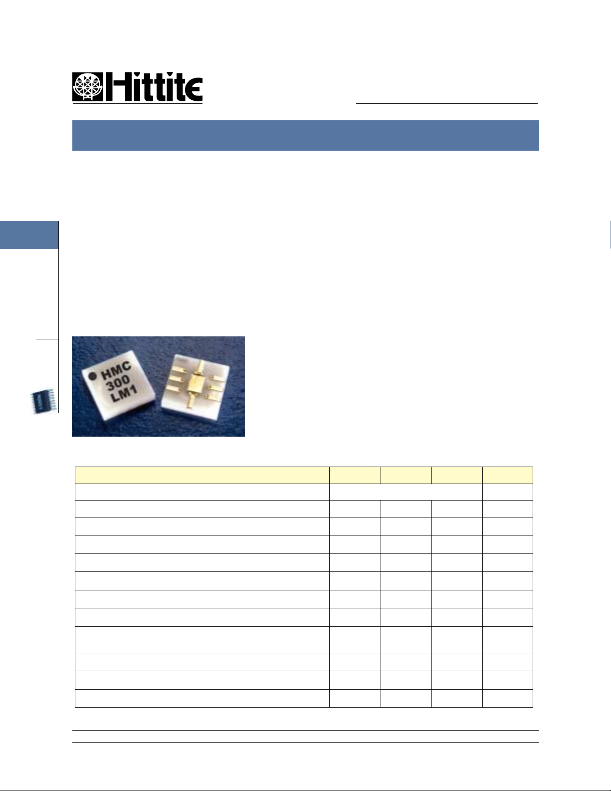
Broadband Gain & Return Loss
25
20
15
10
5
0
-5
RESPONSE (dB)
-10
-15
-20
-25
20 25 30 35 40
FREQUENCY (GHz)
S21
S11
S22
Input Return Loss vs.
Temperature @ Vdd= +6V
0
-5
-10
FEBRUARY 2001
Gain vs. Temperature @ Vdd= +6V
25
20
15
GAIN (dB)
10
+25 C
5
0
24 25 26 27 28 29 30 31 32 33 34 35
+85 C
-40 C
FREQUENCY (GHz)
Output Return Loss vs.
Temperature @ Vdd= +6V
0
-5
-10
1
AMPLIFIERS
SMT
RETURN LOSS (dB)
-15
-20
24 25 26 27 28 29 30 31 32 33 34 35
+25 C
+85 C
-40 C
FREQUENCY (GHz)
P1dB Output Power vs.
Temperature @ Vdd= +6V
30
25
20
15
10
Output P1dB (dBm)
5
0
24 25 26 27 28 29 30 31 32 33 34 35
+25 C
+85 C
-40 C
FREQUENCY (GHz)
RETURN LOSS (dB)
-15
-20
24 25 26 27 28 29 30 31 32 33 34 35
FREQUENCY (GHz)
+25 C
+85 C
-40 C
Output IP3 vs.
Temperature @ Vdd= +6V
35
30
25
20
15
10
5
THIRD ORDER INTERCEPT POINT (dBm)
0
24 25 26 27 28 29 30 31 32 33 34 35
+25 C
+85 C
-40 C
FREQUENCY (GHz)
12 Elizabeth Drive, Chelmsford, MA 01824 Phone: 978-250-3343 Fax: 978-250-3373 Web Site: www.hittite.com
1 - 95
Page 3
MICROWAVE CORPORATION
SMT MEDIUM POWER AMPLIFIER 25.5 - 33.5 GHz
HMC300LM1
FEBRUARY 2001
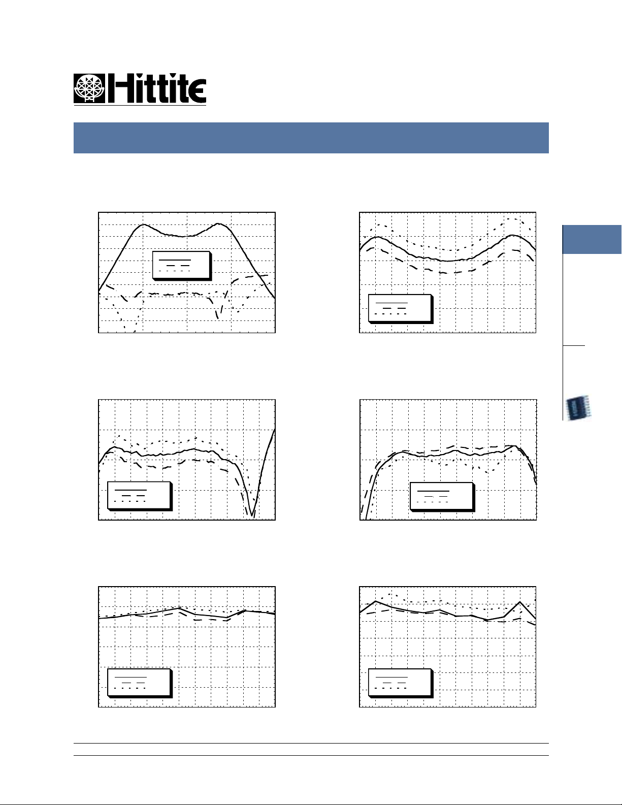
Gain vs. Vdd
1
GAIN (dB)
AMPLIFIERS
SMT
Output Return Loss vs. Vdd
25
20
15
10
Vdd=+5V
5
0
24 25 26 27 28 29 30 31 32 33 34 35
0
-5
-10
Vdd=+6V
Vdd=+7V
FREQUENCY (GHz)
Input Return Loss vs. Vdd
0
-5
-10
RETURN LOSS (dB)
-15
-20
24 25 26 27 28 29 30 31 32 33 34 35
Vdd=+5V
Vdd=+6V
Vdd=+7V
FREQUENCY (GHz)
P1dB Output Power vs. Vdd
30
25
20
15
V00.1200
10
RETURN LOSS (dB)
-15
-20
24 25 26 27 28 29 30 31 32 33 34 35
FREQUENCY (GHz)
Vdd=+5V
Vdd=+6V
Vdd=+7V
Output P1dB (dBm)
5
0
24 25 26 27 28 29 30 31 32 33 34 35
Vdd=+5V
Vdd=+6V
Vdd=+7V
FREQUENCY (GHz)
Psat Output Power vs. Vdd IP3 vs. Vdd
30
25
20
15
Psat (d Bm)
10
5
0
24 25 26 27 28 29 30 31 32 33 34 35
Vdd=+5V
Vdd=+6V
Vdd=+7V
FREQUENCY (GHz)
12 Elizabeth Drive, Chelmsford, MA 01824 Phone: 978-250-3343 Fax: 978-250-3373 Web Site: www.hittite.com
35
30
25
20
15
10
5
THIRD ORDER INTERCEPT POINT (dBm)
0
24 25 26 27 28 29 30 31 32 33 34 35
Vdd=+5V
Vdd=+6V
Vdd=+7V
FREQUENCY (GHz)
1 - 96
Page 4

MICROWAVE CORPORATION
SMT MEDIUM POWER AMPLIFIER 25.5 - 33.5 GHz
HMC300LM1
V00.1200
Functional Diagram
Note:
Dashed lines
represent I/Os
on bottom of
package.
Outline
(
Bottom View)
(Top View)
FEBRUARY 2001
Absolute Maximum Ratings
)ddV(egatloVylppuScdV8+
)ddI(tnerruCylppuSAm005
)ggV(egatloVsaiBetaGV4.0+ot0.2-
rewoPtupnImBd01+
o
o
/Wm30.51etareD
erutarepmeTegarotS051+ot56-
erutarepmeTgnitarepO58+ot04-
o
58evobaC
C
)C
58=aT(ssidPsuounitnoC
Note: Use HMC marking
and dot to establish proper
orientation.
Wm3531
o
C
o
C
1
AMPLIFIERS
SMT
1. MATERIAL:
A) PACKAGE BODY & LID: PLASTIC.
B) PIN CONTACT : COPPER, 0.5 OUNCE.
2. PLATING : ELECTROLYTIC GOLD (50-225 MICROINCHES) OVER
ELECTROLYTIC NICKEL (75 TO 225 MICROINCHES).
3. DIMENSIONS ARE IN INCHES (MILLIMETERS).UNLESS OTHERWISE SPECIFIED
ALL TOLERANCES ARE ± 0.005 (± 0.13).
4. ALL GROUNDS MUST BE SOLDERED TO THE PCB RF GROUND.
5. SEE APPLICATION NOTE FOR RECOMMENDED ATTACHMENT TECHNIQUE TO PCB.
12 Elizabeth Drive, Chelmsford, MA 01824 Phone: 978-250-3343 Fax: 978-250-3373 Web Site: www.hittite.com
1 - 97
Page 5

MICROWAVE CORPORATION
SMT MEDIUM POWER AMPLIFIER 25.5 - 33.5 GHz
HMC300LM1
FEBRUARY 2001
HMC300LM1 Evaluation PCB
1
AMPLIFIERS
SMT
V00.1200
The grounded Co-Planar Wave Guide (G-CPW) PCB input/output transitions allows use of Ground-SignalGround (GSG) probes for testing. Suggested probe pitch is 400µm (16 mils). Alternatively, the board can
be mounted in a metal housing with 2.4 mm coaxial connectors.
Evaluation Circuit Board Layout Design Details
euqinhceTtuoyaLWPC-GotpirtSorciM
lairetaMuC,zo2/1htiw3004sregoR
ssenkcihTcirtceleiD)mm02.0("800.0
htdiWeniLpirtsorciM)mm64.0("810.0
htdiWeniLWPC-G)mm14.0("610.0
paGDNGoteniLWPC-G)mm31.0("500.0
remaiDeloHaiVdnuorG)mm31.0("800.0
1C.gkP2040,roticapaCFp001
2C.gkP6021,roticapaCFp000,33
LM1 package mounted to evaluation PCB
12 Elizabeth Drive, Chelmsford, MA 01824 Phone: 978-250-3343 Fax: 978-250-3373 Web Site: www.hittite.com
1 - 98
Page 6

MICROWAVE CORPORATION
SMT MEDIUM POWER AMPLIFIER 25.5 - 33.5 GHz
HMC300LM1
V00.1200
HMC300LM1 Application Circuit
C1
Vdd1
C2
Vdd2
HMC300LM1
Vgg1
C2
C2
C1
C1
RF OUT
FEBRUARY 2001
1
AMPLIFIERS
SMT
seulaVtnenopmoCdednemmoceR
1CFp001
2CFp000,33
12 Elizabeth Drive, Chelmsford, MA 01824 Phone: 978-250-3343 Fax: 978-250-3373 Web Site: www.hittite.com
Note: Vgg1 should be applied to Pin 6 to provide appropriate
bias level to Amplifier. Voltage level should be adjusted until
nominal Idd of 200 mA is reached.
1 - 99
Page 7

MICROWAVE CORPORATION
SMT MEDIUM POWER AMPLIFIER 25.5 - 33.5 GHz
HMC300LM1
FEBRUARY 2001
HMC300LM1 Recommended SMT Attachment Technique
Preparation & Handling of the LM1 Millimeterwave Package for Surface Mounting
1
The HMC LM1 package was designed to be compatible with
high volume surface mount PCB assembly processes. The
LM1 package requires a specific mounting pattern to allow
proper mechanical attachment and to optimize electrical
performance at millimeterwave frequencies. This PCB layout
pattern can be found on each LM1 product data sheet. It can
also be provided as an electronic drawing upon request from
Hittite Sales & Application Engineering.
Follow these precautions to avoid permanent damage:
AMPLIFIERS
Cleanliness:
clean devices and PCBs. LM1 devices should remain in their
original packaging until component placement to ensure no
contamination or damage to RF, DC & ground contact areas.
Static Sensitivity:
ESD strikes ( see catalog page 8 - 2 ).
SMT
General Handling:
vacuum collet or along the edges with a sharp pair of bent
tweezers. Avoiding damaging the RF, DC, & ground contacts on the package bottom. Do not apply excess pressure
to the top of the lid.
Solder Materials & Temperature Profile:
not recommended. Conductive epoxy attachment is not recommended.
Solder Paste
Solder paste should be selected based on the user’s experience and be compatible with the metallization systems
used. See the LM1 data sheet Outline drawing for pin & ground contact metallization schemes.
Observe proper handling procedures to ensure
Follow ESD precautions to protect against
Handle the LM1 package on the top with a
Follow the information contained in the application note. Hand soldering is
225
200
175
C)
0
150
125
100
TEMPERATURE (
75
50
25
012345678
Recommended solder reflow profile
for HMC LM1 SMT package
TIME (min)
V00.1200
Solder Paste Application
Solder paste is generally applied to the PCB using either a stencil printer or dot placement. The volume of solder
paste will be dependent on PCB and component layout and should be controlled to ensure consistent mechanical
& electrical performance. Excess solder may create unwanted electrical parasitics at high frequencies.
Solder Reflow
The soldering process is usually accomplished in a reflow oven but may also use a vapor phase process. A solder
reflow profile is suggested above.
Prior to reflowing product, temperature profiles should be measured using the same mass as the actual assemblies.
The thermocouple should be moved to various positions on the board to account for edge and corner effects and
varying component masses. The final profile should be determined by mounting the thermocouple to the PCB at the
location of the device.
Follow solder paste and oven vendor’s recommendations when developing a solder reflow profile. A standard
profile will have a steady ramp up from room temperature to the pre-heat temperature to avoid damage due to
thermal shock. Allow enough time between reaching pre-heat temperature and reflow for the solvent in the paste to
evaporate and the flux to completely activate. Reflow must then occur prior to the flux being completely driven off.
The duration of peak reflow temperature should not exceed 15 seconds. Packages have been qualified to withstand a peak temperature of 235°C for 15 seconds. Verify that the profile will not expose device to temperatures in
excess of 235°C.
Cleaning
A water-based flux wash may be used.
12 Elizabeth Drive, Chelmsford, MA 01824 Phone: 978-250-3343 Fax: 978-250-3373 Web Site: www.hittite.com
1 - 100
Page 8

MICROWAVE CORPORATION
SMT MEDIUM POWER AMPLIFIER 25.5 - 33.5 GHz
HMC300LM1
V00.1200
NOTES:
FEBRUARY 2001
1
AMPLIFIERS
SMT
12 Elizabeth Drive, Chelmsford, MA 01824 Phone: 978-250-3343 Fax: 978-250-3373 Web Site: www.hittite.com
1 - 101
 Loading...